
ADC0832
AD转换芯片ADC0832的应用
原创(本文曾刊载于《电子制作》第 142期)
V2.0 2007.2.11
目录
1. 概要 (1)
1.1 简介 (1)
1.2 接口示意图 (1)
1.3 芯片接口说明 (1)
2. 单片机对ADC0832的控制原理 (2)
2.1 ADC0832与单片机的接口电路 (2)
3. ADC0832芯片接口程序的编写 (4)
3.1 ADC0832数据读取程序流程 (4)
3.2 ADC0832芯片接口程序[汇编] (4)
版本信息 (6)
原创 1. 概要
1.1 简介
ADC0832是美国国家半导体公司生产的一种8位分辨率、双通道A/D转换芯片。
由于它体积小,兼容性强,性价比高而深受单片机爱好者及企业欢迎,其目前已经有很高的普及率。
学习并使用
ADC0832可是使我们了解A/D转换器的原理,有助于我们单片机技术水平的提高。
ADC0832具有以下特点:
8位分辨率;
双通道A/D转换;
输入输出电平与TTL/CMOS相兼容;
5V电源供电时输入电压在0~5V之间;
工作频率为250KHZ,转换时间为32μS;
一般功耗仅为15mW;
8P、14P—DIP(双列直插)、PICC多种封装;
商用级芯片温宽为0°C to +70°C−
,工业级芯片温宽为40°C to +85°C;
1.2 接口示意图
1.3 芯片接口说明
CS_ 片选使能,低电平芯片使能。
CH0 模拟输入通道0,或作为IN+/-使用。
CH1 模拟输入通道1,或作为IN+/-使用。
GND 芯片参考0电位(地)。
DI 数据信号输入,选择通道控制。
DO 数据信号输出,转换数据输出。
CLK 芯片时钟输入。
Vcc/REF 电源输入及参考电压输入(复用)。
原创 2. 单片机对ADC0832的控制原理
2.1 ADC0832与单片机的接口电路
ADC0832为8位分辨率A/D转换芯片,其最高分辨可达256级,可以适应一般的模拟量转换要求。
其内部电源输入与参考电压的复用,使得芯片的模拟电压输入在0~5V之间。
芯片转换时间仅
为32μS,据有双数据输出可作为数据校验,以减少数据误差,转换速度快且稳定性能强。
独立的
芯片使能输入,使多器件挂接和处理器控制变的更加方便。
通过DI数据输入端,可以轻易的实现
通道功能的选择。
正常情况下ADC0832与单片机的接口应为4条数据线,分别是CS、CLK、DO、DI。
但由于DO端与DI端在通信时并未同时有效并与单片机的接口是双向的,所以电路设计时可以将DO和DI并联
在一根数据线上使用。
当ADC0832未工作时其CS输入端应为高电平,此时芯片禁用,CLK和DO/DI的电平可任意。
当要进行A/D转换时,须先将CS使能端置于低电平并且保持低电平直到转换完全结束。
此时芯片开
始转换工作,同时由处理器向芯片时钟输入端CLK输入时钟脉冲,DO/DI端则使用DI端输入通道功
能选择的数据信号。
在第1个时钟脉冲的下沉之前DI端必须是高电平,表示启始信号。
在第2、3
个脉冲下沉之前DI端应输入2位数据用于选择通道功能,其功能项见表1。
原创
表1
如表1所示,当此2位数据为“1”、“0”时,只对CH0进行单通道转换。
当2位数据为“1”、“1”时,只对CH1进行单通道转换。
当2位数据为“0”、“0”时,将CH0作为正输入端IN+,CH1作为负输入端IN-进行输入。
当2位数据为“0”、“1”时,将CH0作为负输入端IN-,CH1作为正输入端IN+进行输入。
到第3个脉冲的下沉之后DI端的输入电平就失去输入作用,此后DO/DI端则开始利用数据输出DO进行转换数据的读取。
从第4个脉冲下沉开始由DO端输出转换数据最高位DATA7,随后每一个脉冲下沉DO端输出下一位数据。
直到第11个脉冲时发出最低位数据DATA0,一个字节的数据输出完成。
也正是从此位开始输出下一个相反字节的数据,即从第11个字节的下沉输出DATD0。
随后输出8位数据,到第19个脉冲时数据输出完成,也标志着一次A/D转换的结束。
最后将CS置高电平禁用芯片,直接将转换后的数据进行处理就可以了。
更详细的时序说明请见表2。
表2
原创
作为单通道模拟信号输入时ADC0832的输入电压是0~5V且8位分辨率时的电压精度为19.53mV。
如果作为由IN+与IN-输入的输入时,可是将电压值设定在某一个较大范围之内,从而提高转换的宽度。
但值得注意的是,在进行IN+与IN-的输入时,如果IN-的电压大于IN+的电压则转换后的数据结果始终为00H。
原创
MOV A,B
MOV C,ACC.1 ;确定取值通道选择
MOV ADDI,C
NOP
NOP
SETB ADCLK ;拉高CLK端
NOP
NOP
CLR ADCLK ;拉低CLK端,形成下降沿2
MOV A,B
MOV C,ACC.0 ;确定取值通道选择
MOV ADDI,C
NOP
NOP
SETB ADCLK ;拉高CLK端
NOP
NOP
CLR ADCLK ;拉低CLK端,形成下降沿3
SETB ADDI
NOP
NOP
MOV R7,#8 ;准备送下后8个时钟脉冲
AD_1:
MOV C,ADDO ;接收数据
MOV ACC.0,C
RL A ;左移一次
SETB ADCLK
NOP
NOP
CLR ADCLK ;形成一次时钟脉冲
NOP
NOP
DJNZ R7,AD_1 ;循环8次
MOV C,ADDO ;接收数据
MOV ACC.0,C
MOV B,A
MOV R7,#8
AD_13:
MOV C,ADDO ;接收数据
MOV ACC.0,C
RR A ;左移一次
SETB ADCLK
NOP
NOP
CLR ADCLK ;形成一次时钟脉冲
NOP
NOP
DJNZ R7,AD_13 ;循环8次
CJNE A,B,ADCONV ;数据校验
SETB ADCS ;拉高/CS端
CLR ADCLK ;拉低CLK端
SETB ADDO ;拉高数据端,回到初始状态
RET
;====子程序结束====
原创
题目 AD转换芯片ADC0832的应用
作者 杜洋 (本文曾刊载于《电子制作》第 142期)
版本 2005-10-11 V1.0 / 2007-2-11 V2.0
声明 本站内容(包括程序代码、文档、照片、视频等)属个人所有,未经网站作者同意请勿转载或引用,对于 转载或复制而造成的任何不良后果概不负责。
对于本站内免费下载的资料、图片及视频不能保证其真实可 靠,对于免费下载的程序代码本站作者不给矛技术支持和服务。
标注ST2007-2-11D0832。
ADC0832

ADC0832设计模块1、ADC0832的主要技术指标:(1)8位分辨率,逐次逼近型。
(2)5V电源供电时,基准电压为5V,输入模拟电压范围为0~5V。
(3)输入和输出电平与TTL和CMOS兼容。
(4)有两个可供选择的模拟输入通道。
(5)在250KHz时钟频率时,转换时间为32µs。
(6)一般功耗仅为15mW。
2、ADC0832引脚说明(1)/CS片选使能,低电平有效。
(2)CHO模拟通道0,差分输入时,作为IN+或IN-使用。
(3)CH1模拟输入通道1,差分输入时,作为IN+或IN-使用。
(4)GND 电源地。
(5)DI数据信号输出,选择通道控制。
(6)DO数据信号输出,转换数据输出。
(7)Vcc/Vre电源输入及参考电压输入(复用)。
(8)CLK芯片时钟信号3、ADC0832时序图4、运用ADC0832设计一个0-5V的数字电压表电路如图所示:设计要求:五位数码管动态显示,第一位显示通道状态(0、1)第二位显示C,第三位是个数,第三位和第四位数码管分别显示十分位和百分位;按键SW1选择通道0,按键SW2选择通道1,并且蜂鸣器和短时间鸣叫;调节滑动变阻器数码管的示数能在0.00~5.00之间变化。
C程序:/************************************************CAUCyeyongan*************************************************/#include <reg52.h>#include <intrins.h>#define uchar unsigned charsbit CS=P3^5;sbit Clk=P1^6; //时钟sbit DO=P3^7; //ADC0832输出引脚sbit DI=P3^6; //ADC0832输入引脚sbit key=P3^3; //按键bit keydownflg; //操作位的定义bit adc_flg;uchar dat,channel;uchar key_buffer;uchar P2_buffer;uchar Beep_cnt;uchar disp_cnt;uchar count4ms;uchar disp_buff[5]; //数码管显示缓存uchar code Tab1[]={0xC0,0xF9,0xA4,0xB0,0x99,0x92,0x82,0xF8,0x80,0x90,0x88,0x83,0xA7,0 xA1,0x86,0x8E}; //共阳数码表uchar code Tab[5]={0x7f,0xbf,0xdf,0xef,0xf7}; //数码管位选表uchar A_D(uchar CH) //AD函数{uchar i,adval,test; //定义局部变量并初始化adval=0x00;test=0x00;Clk=0; //clk低电平DI=1; //DI初始高电平在第一个时钟脉冲的下降沿前保持高电平,表示启动信号_nop_();CS=0; //片选_nop_();Clk=1; //clk上升沿,起始位写入_nop_();if(CH==0x00) //选择通道0{Clk=0; //clk低电平DI=1;_nop_();Clk=1; //clk上升沿,通道0的第一位写入_nop_();Clk=0;DI=0;_nop_();Clk=1; //clk上升沿,通道0的第二位写入_nop_();}else{Clk=0;DI=1;_nop_();Clk=1; //clk上升沿,通道1的第一位写入_nop_();Clk=0;DI=1;_nop_(); //clk上升沿,通道1的第二位写入Clk=1;_nop_();}Clk=0;DI=1;for(i=0;i<8;i++) //从高位向低位读取八位AD值{_nop_();adval<<=1;Clk=1;_nop_();Clk=0;if(DO)adval|=0x01;elseadval|=0x00;}for(i=0;i<8;i++){test>>=1; //从低位向高位读取八位AD值if(DO)test|=0x80;elsetest|=0x00;_nop_();Clk=1;_nop_();Clk=0;}if(adval==test) dat=test; //判断两个读取值是否相等相等就把读取的数赋值给DAT_nop_();CS=1;DO=1;Clk=1;return dat;}void FillDispBuffer(void) //数码管显示缓存函数{disp_buff[0]=channel; //显示通道disp_buff[1]=12; //显示"C"disp_buff[2]=dat/51; //显示个位disp_buff[3]=dat%51*10/51; //显示十分位disp_buff[4]=((dat%51)*10%51)*10/51; //显示百分位}void dealkey(void) //按键处理{if(keydownflg) return; //keydownflg控制位为1,不对按键进行处理key_buffer=P2;if((key_buffer&0x80)!=0x80) channel=0; //选择通道0if((key_buffer&0x40)!=0x40) channel=1; //选择通道1FillDispBuffer(); //数码管显示缓存Beep_cnt=0;keydownflg=1; //keydownflg控制位置1 }void main(void) //主函数{P0=0xff; //初始化P2=0xff;dat=0x00;disp_cnt=0;count4ms=0;channel=0;TMOD=0x10;TH0=(65535-4000)/256;TL0=(65535-4000)%256;EA=1;TR0=1;ET0=1;while(1){if(adc_flg) //ADC转换控制位,防止输入与输出产生冲突{adc_flg=0;A_D(channel); //ADC函数FillDispBuffer(); //数码管显示缓存}if(!key) //按键dealkey();}}void T0_service(void) interrupt 1 //定时器0中断子函数{TH0=(65535-4000)/256;TL0=(65535-4000)%256;P2_buffer=Tab[disp_cnt]; //查表,数码管的位选择if(keydownflg) //蜂鸣器0.4s的短时间鸣叫{P2_buffer=P2_buffer&0xfe;Beep_cnt++;if(Beep_cnt==100) keydownflg=0;}P2=P2_buffer; //数码管显示数字符号if(disp_cnt==2) //第三位数码管显示小数点P0=Tab1[disp_buff[disp_cnt]]&0x7f;elseP0=Tab1[disp_buff[disp_cnt]];disp_cnt++; //if(disp_cnt==5) disp_cnt=0;count4ms++;if(count4ms==50) //0.2s ADC转换一次{adc_flg=1;count4ms=0;}}。
ADC0832

ADC0831/ADC0832/ADC0834/ADC08388-Bit Serial I/O A/D Converters with Multiplexer OptionsGeneral DescriptionThe ADC0831series are 8-bit successive approximation A/D converters with a serial I/O and configurable input multiplex-ers with up to 8channels.The serial I/O is configured to comply with the NSC MICROWIRE ™serial data exchange standard for easy interface to the COPS ™family of proces-sors,and can interface with standard shift registers or µPs.The 2-,4-or 8-channel multiplexers are software configured for single-ended or differential inputs as well as channel as-signment.The differential analog voltage input allows increasing the common-mode rejection and offsetting the analog zero input voltage value.In addition,the voltage reference input can be adjusted to allow encoding any smaller analog voltage span to the full 8bits of resolution.Featuresn NSC MICROWIRE compatible —direct interface to COPS family processorsn Easy interface to all microprocessors,or operates “stand-alone”n Operates ratiometrically or with 5V DC voltage referencen No zero or full-scale adjust requiredn 2-,4-or 8-channel multiplexer options with address logic n Shunt regulator allows operation with high voltage suppliesn 0V to 5V input range with single 5V power supply n Remote operation with serial digital data link n TTL/MOS input/output compatiblen 0.3"standard width,8-,14-or 20-pin DIP package n 20Pin Molded Chip Carrier Package (ADC0838only)n Surface-Mount PackageKey Specificationsn Resolution8Bitsn Total Unadjusted Error ±1⁄2LSB and ±1LSBn Single Supply 5V DC n Low Power15mW nConversion Time32µsTypical ApplicationTRI-STATE ®is a registered trademark of National Semiconductor Corporation.COPS ™and MICROWIRE ™are trademarks of National Semiconductor Corporation.DS005583-1August 1999ADC0831/ADC0832/ADC0834/ADC08388-Bit Serial I/O A/D Converters with Multiplexer Options©1999National Semiconductor Corporation Connection DiagramsADC08388-Channel MuxSmall Outline/Dual-In-Line Package(WM and N)DS005583-8Top ViewADC08344-Channel MUXSmall Outline/Dual-In-Line Package(WM and N)DS005583-30COM internally connected to A GND Top ViewTop ViewADC08322-Channel MUX Dual-In-Line Package (N)DS005583-31COM internally connected to GND.V REF internally connected to V CC .Top ViewTop ViewADC08322-Channel MUX Small Outline Package (WM)DS005583-41Top ViewADC0831Single Differential Input Dual-In-Line Package (N)DS005583-32Top ViewADC0831Single Differential Input Small Outline Package (WM)DS005583-42Top ViewADC08388-Channel MUX Molded Chip Carrier (PCC)Package (V)DS005583-33 2Ordering InformationPart Number Analog Input Total Package TemperatureChannels Unadjusted Error RangeADC0831CCN1±1Molded(N)0˚C to+70˚CADC0831CCWM SO(M)0˚C to+70˚CADC0832CIWM2±1SO(M)−40˚C to+85˚CADC0832CCN Molded(N)0˚C to+70˚CADC0832CCWM SO(M)0˚C to+70˚CADC0834BCN4±1⁄2Molded(N)0˚C to+70˚CADC0834CCN±1Molded(N)0˚C to+70˚CADC0834CCWM SO(M)0˚C to+70˚CADC0838BCV8±1⁄2PCC(V)0˚C to+70˚CADC0838CCV±1PCC(V)0˚C to+70˚CADC0838CCN Molded(N)0˚C to+70˚CADC0838CIWM SO(M)−40˚C to+85˚CADC0838CCWM SO(M)0˚C to+70˚CSee NS Package Number M14B,M20B,N08E,N14A,N20A or V20A3Absolute Maximum Ratings(Notes1,2) If Military/Aerospace specified devices are required, please contact the National Semiconductor Sales Office/ Distributors for availability and specifications.Current into V+(Note3)15mA Supply Voltage,V CC(Note3) 6.5V VoltageLogic Inputs−0.3V to V CC+0.3V Analog Inputs−0.3V to V CC+0.3V Input Current per Pin(Note4)±5mA Package±20mA Storage Temperature−65˚C to+150˚C Package Dissipationat T A=25˚C(Board Mount)0.8W Lead Temperature(Soldering10sec.)Dual-In-Line Package(Plastic)260˚C Molded Chip Carrier PackageVapor Phase(60sec.)215˚C Infrared(15sec.)220˚C ESD Susceptibility(Note5)2000V Operating Ratings(Notes1,2)Supply Voltage,V CC 4.5V DC to6.3V DC Temperature Range T MIN≤T A≤T MAX ADC0832/8CIWM−40˚C to+85˚C ADC0834BCN,ADC0838BCV,ADC0831/2/4/8CCN,ADC0838CCV,ADC0831/2/4/8CCWM0˚C to+70˚CConverter and Multiplexer Electrical Characteristics The following specifications apply for V CC=V+=V REF=5V,V REF≤V CC+0.1V,T A=T j=25˚C,and f CLK=250kHz unless otherwise specified.Boldface limits apply from T MIN to T MAX.Parameter Conditions CIWM Devices BCV,CCV,CCWM,BCNand CCN DevicesTyp Tested Design Typ Tested Design Units (Note12)Limit Limit(Note12)Limit Limit(Note13)(Note14)(Note13)(Note14)CONVERTER AND MULTIPLEXER CHARACTERISTICSTotal Unadjusted Error V REF=5.00VADC0838BCV(Note6)±1⁄2±1⁄2ADC0834BCN±1⁄2±1⁄2LSB(Max) ADC0838CCV±1±1ADC0831/2/4/8CCN±1±1ADC0831/2/4/8CCWM±1±1ADC0832/8CIWM±1Minimum Reference 3.5 1.3 3.5 1.3 1.3kΩInput Resistance(Note7)Maximum Reference 3.5 5.9 3.5 5.4 5.9kΩInput Resistance(Note7)Maximum Common-ModeInput Range(Note8)V CC+0.05V CC+0.05V CC+0.05VMinimum Common-ModeInput Range(Note8)GND−0.05GND−0.05GND−0.05V DC Common-Mode Error±1/16±1⁄4±1/16±1⁄4±1⁄4LSB Change in zero15mA into V+error from V CC=5V V CC=N.C.to internal zener V REF=5Voperation(Note3)111LSB V Z,internal MIN15mA into V+ 6.3 6.3 6.3diode breakdown MAX8.58.58.5V (at V+)(Note3)Power Supply Sensitivity V CC=5V±5%±1/16±1⁄4±1⁄4±1/16±1⁄4±1⁄4LSBI OFF,Off Channel Leakage On Channel=5V,−0.2−0.2−1µACurrent(Note9)Off Channel=0V−1On Channel=0V,+0.2+0.2+1µAOff Channel=5V+14Converter and Multiplexer Electrical Characteristics The following specifications apply for V CC=V+=V REF=5V,V REF≤V CC+0.1V,T A=T j=25˚C,and f CLK=250kHz unless otherwise specified.Boldface limits apply from T MIN to T MAX.(Continued)Parameter Conditions CIWM Devices BCV,CCV,CCWM,BCNand CCN DevicesTyp Tested Design Typ Tested Design Units (Note12)Limit Limit(Note12)Limit Limit(Note13)(Note14)(Note13)(Note14)CONVERTER AND MULTIPLEXER CHARACTERISTICSI ON,On Channel Leakage On Channel=0V,−0.2−0.2−1µA Current(Note9)Off Channel=5V−1On Channel=5V,+0.2+0.2+1µAOff Channel=0V+1DIGITAL AND DC CHARACTERISTICSV IN(1),Logical“1”Input V CC=5.25V 2.0 2.0 2.0V Voltage(Min)V IN(0),Logical“0”Input V CC=4.75V0.80.80.8V Voltage(Max)I IN(1),Logical“1”Input V IN=5.0V0.00510.00511µA Current(Max)I IN(0),Logical“0”Input V IN=0V−0.005−1−0.005−1−1µA Current(Max)V OUT(1),Logical“1”Output V CC=4.75VVoltage(Min)I OUT=−360µA 2.4 2.4 2.4VI OUT=−10µA 4.5 4.5 4.5VV OUT(0),Logical“0”Output V CC=4.75V0.40.40.4V Voltage(Max)I OUT=1.6mAI OUT,TRI-STATE Output V OUT=0V−0.1−3−0.1−3−3µA Current(Max)V OUT=5V0.130.1+3+3µAI SOURCE,Output Source V OUT=0V−14−6.5−14−7.5−6.5mA Current(Min)I SINK,Output Sink Current(Min)V OUT=V CC168.0169.08.0mAI CC,Supply Current(Max)ADC0831,ADC0834,0.9 2.50.9 2.5 2.5mA ADC0838ADC0832Includes Ladder 2.3 6.5 2.3 6.5 6.5mACurrentAC CharacteristicsThe following specifications apply for V CC=5V,t r=t f=20ns and25˚C unless otherwise specified.Typ Tested Design Limit Parameter Conditions(Note12)Limit Limit Units(Note13)(Note14)f CLK,Clock Frequency Min10kHzMax400kHzt C,Conversion Time Not including MUX Addressing Time81/f CLK Clock Duty Cycle Min40% (Note10)Max60%t SET-UP,CS Falling Edge or250ns Data Input Valid to CLKRising Edget HOLD,Data Input Valid90ns after CLK Rising Edge5AC Characteristics(Continued)The following specifications apply for V CC =5V,t r =t f =20ns and 25˚C unless otherwise specified.TypTested Design Limit ParameterConditions(Note 12)Limit Limit Units(Note 13)(Note 14)t pd1,t pd0—CLK Falling C L =100pF Edge to Output Data Valid Data MSB First 6501500ns (Note 11)Data LSB First 250600ns t 1H ,t 0H ,—Rising Edge of C L =10pF,R L =10k125250ns CS to Data Output and (see TRI-STATE ®Test Circuits)SARS Hi–ZC L =100pf,R L =2k500ns C IN ,Capacitance of Logic 5pF InputC OUT ,Capacitance of Logic 5pFOutputsNote 1:Absolute Maximum Ratings indicate limits beyond which damage to the device may occur.DC and AC electrical specifications do not apply when operating the device beyond its specified operating conditions.Note 2:All voltages are measured with respect to the ground plugs.Note 3:Internal zener diodes (6.3to 8.5V)are connected from V+to GND and V CC to GND.The zener at V+can operate as a shunt regulator and is connected to V CC via a conventional diode.Since the zener voltage equals the A/D’s breakdown voltage,the diode insures that V CC will be below breakdown when the device is powered from V+.Functionality is therefore guaranteed for V+operation even though the resultant voltage at V CC may exceed the specified Absolute Max of 6.5V.It is recommended that a resistor be used to limit the max current into V+.(See Figure 3in Functional Description Section 6.0)Note 4:When the input voltage (V IN )at any pin exceeds the power supply rails (V IN <V −or V IN >V +)the absolute value of current at that pin should be limited to 5mA or less.The 20mA package input current limits the number of pins that can exceed the power supply boundaries with a 5mA current limit to four.Note 5:Human body model,100pF discharged through a 1.5k Ωresistor.Note 6:Total unadjusted error includes offset,full-scale,linearity,and multiplexer errors.Note 7:Cannot be tested for ADC0832.Note 8:For V IN (−)≥V IN (+)the digital output code will be 00000000.Two on-chip diodes are tied to each analog input (see Block Diagram)which will forward conduct for analog input voltages one diode drop below ground or one diode drop greater than the V CC supply.Be careful,during testing at low V CC levels (4.5V),as high level analog inputs (5V)can cause this input diode to conduct —especially at elevated temperatures,and cause errors for analog inputs near full-scale.The spec allows 50mV forward bias of either diode.This means that as long as the analog V IN or V REF does not exceed the supply voltage by more than 50mV,the output code will be correct.To achieve an absolute 0V DC to 5V DC input voltage range will therefore require a minimum supply voltage of 4.950V DC over temperature varia-tions,initial tolerance and loading.Note 9:Leakage current is measured with the clock not switching.Note 10:A 40%to 60%clock duty cycle range insures proper operation at all clock frequencies.In the case that an available clock has a duty cycle outside of these limits,the minimum,time the clock is high or the minimum time the clock is low must be at least 1µs.The maximum time the clock can be high is 60µs.The clock can be stopped when low so long as the analog input voltage remains stable.Note 11:Since data,MSB first,is the output of the comparator used in the successive approximation loop,an additional delay is built in (see Block Diagram)to allow for comparator response time.Note 12:Typicals are at 25˚C and represent most likely parametric norm.Note 13:Tested limits are guaranteed to National’s AOQL (Average Outgoing Quality Level).Note 14:Guaranteed but not 100%production tested.These limits are not used to calculate outgoing quality levels.Typical Performance CharacteristicsUnadjusted Offset Error vs V REF VoltageDS005583-43Linearity Error vs V REF VoltageDS005583-44Linearity Error vs TemperatureDS005583-45 6Typical Performance Characteristics(Continued)Leakage Current Test CircuitLinearity Error vs f CLKDS005583-46Power Supply Current vs Temperature (ADC0838,ADC0831,ADC0834)DS005583-47Note:For ADC0832add I REF .Output Current vs TemperatureDS005583-48Power Supply Current vs f CLKDS005583-29DS005583-37TRI-STATE Test Circuits and WaveformsTiming Diagramst 1HDS005583-49t 0HDS005583-50t 1H DS005583-51t 0HDS005583-52Data Input TimingDS005583-24Data Output TimingDS005583-25ADC0831Start Conversion TimingDS005583-26 8Timing Diagrams(Continued)ADC0831TimingDS005583-27*LSB first output not available on ADC0831.ADC0832TimingDS005583-28ADC0834TimingDS005583-59Timing Diagrams(Continued)A D C 0838T i m i n gD S 005583-6*M a k e s u r e c l o c k e d g e #18c l o c k s i n t h e L S B b e f o r e S E i s t a k e n l o w10ADC0838Functional Block DiagramD S 005583-7*S o m e o f t h e s e f u n c t i o n s /p i n s a r e n o t a v a i l a b l e w i t h o t h e r o p t i o n s .N o t e 1:F o r t h e A D C 0834,D 1i s i n p u t d i r e c t l y t o t h e D i n p u t o f S E L E C T 1.S E L E C T 0i s f o r c e d t o a “1”.F o r t h e A D C 0832,D I i s i n p u t d i r e c t l y t o t h e D I i n p u t o f O D D /S I G N .S E L E C T 0i s f o r c e d t o a “0”a n d S E L E C T 1i s f o r c e d t o a “1”.11Functional Description 1.0MULTIPLEXER ADDRESSINGThe design of these converters utilizes a sample-data com-parator structure which provides for a differential analog in-put to be converted by a successive approximation routine. The actual voltage converted is always the difference be-tween an assigned“+”input terminal and a“−”input terminal. The polarity of each input terminal of the pair being con-verted indicates which line the converter expects to be the most positive.If the assigned“+”input is less than the“−”in-put the converter responds with an all zeros output code.A unique input multiplexing scheme has been utilized to pro-vide multiple analog channels with software-configurable single-ended,differential,or a new pseudo-differential option which will convert the difference between the voltage at any analog input and a common terminal.The analog signal con-ditioning required in transducer-based data acquisition sys-tems is significantly simplified with this type of input flexibility. One converter package can now handle ground referenced inputs and true differential inputs as well as signals with some arbitrary reference voltage.A particular input configuration is assigned during the MUX addressing sequence,prior to the start of a conversion.The MUX address selects which of the analog inputs are to be enabled and whether this input is single-ended or differential.In the differential case,it also assigns the polarity of the channels.Differential inputs are restricted to adjacent chan-nel pairs.For example channel0and channel1may be se-lected as a different pair but channel0or1cannot act differ-entially with any other channel.In addition to selecting differential mode the sign may also be selected.Channel0 may be selected as the positive input and channel1as the negative input or vice versa.This programmability is best il-lustrated by the MUX addressing codes shown in the follow-ing tables for the various product options.The MUX address is shifted into the converter via the DI line. Because the ADC0831contains only one differential input channel with a fixed polarity assignment,it does not require addressing.The common input line on the ADC0838can be used as a pseudo-differential input.In this mode,the voltage on this pin is treated as the“−”input for any of the other input channels. This voltage does not have to be analog ground;it can be any reference potential which is common to all of the inputs. This feature is most useful in single-supply application where the analog circuitry may be biased up to a potential other than ground and the output signals are all referred to this potential.TABLE1.Multiplexer/Package OptionsPart Number of Analog Channels Number ofNumber Single-Ended Differential Package PinsADC0831118ADC0832218ADC08344214ADC08388420 12Functional Description(Continued)TABLE2.MUX Addressing:ADC0838Single-Ended MUX ModeMUX Address Analog Single-Ended Channel#SGL/ODD/SELECT01234567COMDIF SIGN101000+−1001+−1010+−1011+−1100+−1101+−1110+−1111+−TABLE3.MUX Addressing:ADC0838Differential MUX ModeMUX Address Analog Differential Channel-Pair#SGL/ODD/SELECT0123DIF SIGN10012345670000+−0001+−0010+−0011+−0100−+0101−+0110−+0111−+TABLE4.MUX Addressing:ADC0834Single-Ended MUX ModeMUX Address Channel#SGL/ODD/SELECTDIF SIGN10123100+101+110+111+COM is internally tied to A GNDTABLE5.MUX Addressing:ADC0834Differential MUX ModeMUX Address Channel#SGL/ODD/SELECTDIF SIGN10123000+−001+−010−+011−+13Functional Description(Continued)TABLE6.MUX Addressing:ADC0832Single-Ended MUX ModeMUX Address Channel#SGL/ODD/01DIF SIGN10+11+COM is internally tied to A GNDTABLE7.MUX Addressing:ADC0832Differential MUX ModeMUX Address Channel#SGL/ODD/01DIF SIGN00+−01−+Since the input configuration is under software control,it can be modified,as required,at each conversion.A channel can be treated as a single-ended,ground referenced input for one conversion;then it can be reconfigured as part of a dif-ferential channel for another conversion.Figure1illustrates the input flexibility which can be achieved.The analog input voltages for each channel can range from 50mV below ground to50mV above V CC(typically5V)with-out degrading conversion accuracy.2.0THE DIGITAL INTERFACEA most important characteristic of these converters is their serial data link with the controlling ing a serial communication format offers two very significant system im-provements;it allows more function to be included in the converter package with no increase in package size and it can eliminate the transmission of low level analog signals by locating the converter right at the analog sensor;transmitting highly noise immune digital data back to the host processor. To understand the operation of these converters it is best to refer to the Timing Diagrams and Functional Block Diagram and to follow a complete conversion sequence.For clarity a separate diagram is shown of each device.1.A conversion is initiated by first pulling the CS(chip select) line low.This line must be held low for the entire conversion. The converter is now waiting for a start bit and its MUX as-signment word.2.A clock is then generated by the processor(if not provided continuously)and output to the A/D clock input.14Functional Description(Continued)3.On each rising edge of the clock the status of the data in (DI)line is clocked into the MUX address shift register.The start bit is the first logic “1”that appears on this line (all lead-ing zeros are ignored).Following the start bit the converter expects the next 2to 4bits to be the MUX assignment word.4.When the start bit has been shifted into the start location of the MUX register,the input channel has been assigned and a conversion is about to begin.An interval of 1⁄2clock pe-riod (where nothing happens)is automatically inserted to al-low the selected MUX channel to settle.The SAR status line goes high at this time to signal that a conversion is now in progress and the DI line is disabled (it no longer accepts data).5.The data out (DO)line now comes out of TRI-STATE and provides a leading zero for this one clock period of MUX set-tling time.6.When the conversion begins,the output of the SAR com-parator,which indicates whether the analog input is greater than (high)or less than (low)each successive voltage from the internal resistor ladder,appears at the DO line on each falling edge of the clock.This data is the result of the conver-sion being shifted out (with the MSB coming first)and can be read by the processor immediately.7.After 8clock periods the conversion is completed.The SAR status line returns low to indicate this 1⁄2clock cycle later.8.If the programmer prefers,the data can be provided in an LSB first format [this makes use of the shift enable (SE)con-trol line].All 8bits of the result are stored in an output shift register.On devices which do not include the SE control line,the data,LSB first,is automatically shifted out the DO line,after the MSB first data stream.The DO line then goes low and stays low until CS is returned high.On the ADC0838the SE line is brought out and if held high,the value of the LSB remains valid on the DO line.When SE is forced low,the data is then clocked out LSB first.The ADC0831is an excep-tion in that its data is only output in MSB first format.9.All internal registers are cleared when the CS line is high.If another conversion is desired,CS must make a high to low transition followed by address information.The DI and DO lines can be tied together and controlled through a bidirectional processor I/O bit with one wire.This is possible because the DI input is only “looked-at”during the MUX addressing interval while the DO line is still in a high impedance state.8Single-EndedDS005583-538Pseudo-DifferentialDS005583-544Differential DS005583-55Mixed ModeDS005583-56FIGURE 1.Analog Input Multiplexer Options for the ADC083815Functional Description(Continued)3.0REFERENCE CONSIDERATIONSThe voltage applied to the reference input to these convert-ers defines the voltage span of the analog input (the differ-ence between V IN(MAX)and V IN(MIN))over which the 256possible output codes apply.The devices can be used in ei-ther ratiometric applications or in systems requiring absolute accuracy.The reference pin must be connected to a voltage source capable of driving the reference input resistance of typically 3.5k Ω.This pin is the top of a resistor divider string used for the successive approximation conversion.In a ratiometric system,the analog input voltage is propor-tional to the voltage used for the A/D reference.This voltage is typically the system power supply,so the V REF pin can be tied to V CC (done internally on the ADC0832).This technique relaxes the stability requirements of the system reference as the analog input and A/D reference move together maintain-ing the same output code for a given input condition.For absolute accuracy,where the analog input varies be-tween very specific voltage limits,the reference pin can be biased with a time and temperature stable voltage source.The LM385and LM336reference diodes are good low cur-rent devices to use with these converters.The maximum value of the reference is limited to the V CC supply voltage.The minimum value,however,can be quite small (see Typical Performance Characteristics)to allow di-rect conversions of transducer outputs providing less than a 5V output span.Particular care must be taken with regard to noise pickup,circuit layout and system error voltage sources when operating with a reduced span due to the increased sensitivity of the converter (1LSB equals V REF /256).4.0THE ANALOG INPUTSThe most important feature of these converters is that they can be located right at the analog signal source and through just a few wires can communicate with a controlling proces-sor with a highly noise immune serial bit stream.This in itself greatly minimizes circuitry to maintain analog signal accu-racy which otherwise is most susceptible to noise pickup.However,a few words are in order with regard to the analog inputs should the input be noisy to begin with or possibly riding on a large common-mode voltage.The differential input of these converters actually reduces the effects of common-mode input noise,a signal common to both selected “+”and “−”inputs for a conversion (60Hz is most typical).The time interval between sampling the “+”in-put and then the “−”input is 1⁄2of a clock period.The change in the common-mode voltage during this short time interval can cause conversion errors.For a sinusoidal common-mode signal this error is:where f CM is the frequency of the common-mode signal,V PEAK is its peak voltage valueand f CLK ,is the A/D clock frequency.For a 60Hz common-mode signal to generate a 1⁄4LSB error (≈5mV)with the converter running at 250kHz,its peak value would have to be 6.63V which would be larger than allowed as it exceeds the maximum analog input limits.Due to the sampling nature of the analog inputs short spikes of current enter the “+”input and exit the “−”input at the clock edges during the actual conversion.These currents decay rapidly and do not cause errors as the internal com-parator is strobed at the end of a clock period.Bypass ca-pacitors at the inputs will average these currents and cause an effective DC current to flow through the output resistance of the analog signal source.Bypass capacitors should not be used if the source resistance is greater than 1k Ω.This source resistance limitation is important with regard to the DC leakage currents of input multiplexer as well.The worst-case leakage current of ±1µA over temperature will create a 1mV input error with a 1k Ωsource resistance.An op amp RC active low pass filter can provide both imped-ance buffering and noise filtering should a high impedance signal source be required.DS005583-57a)Ratiometric DS005583-58b)Absolute with a reduced SpanFIGURE 2.Reference Examples16Functional Description(Continued)5.0OPTIONAL ADJUSTMENTS5.1Zero ErrorThe zero of the A/D does not require adjustment.If the mini-mum analog input voltage value,V IN(MIN),is not ground a zero offset can be done.The converter can be made to out-put00000000digital code for this minimum input voltage by biasing any V IN(−)input at this V IN(MIN)value.This utilizes the differential mode operation of the A/D.The zero error of the A/D converter relates to the location of the first riser of the transfer function and can be measured by grounding the V IN(−)input and applying a small magnitude positive voltage to the V IN(+)input.Zero error is the differ-ence between the actual DC input voltage which is neces-sary to just cause an output digital code transition from0000 0000to00000001and the ideal1⁄2LSB value(1⁄2LSB=9.8 mV for V REF=5.000V DC).5.2Full-ScaleThe full-scale adjustment can be made by applying a differ-ential input voltage which is11⁄2LSB down from the desired analog full-scale voltage range and then adjusting the mag-nitude of the V REF input(or V CC for the ADC0832)for a digi-tal output code which is just changing from11111110to1111 1111.5.3Adjusting for an Arbitrary Analog Input Voltage RangeIf the analog zero voltage of the A/D is shifted away from ground(for example,to accommodate an analog input signal which does not go to ground),this new zero reference should be properly adjusted first.A V IN(+)voltage which equals this desired zero reference plus1⁄2LSB(where the LSB is calculated for the desired analog span,using1LSB= analog span/256)is applied to selected“+”input and the zero reference voltage at the corresponding“−”input should then be adjusted to just obtain the00HEX to01HEX code tran-sition.The full-scale adjustment should be made[with the proper V IN(−)voltage applied]by forcing a voltage to the V IN(+)in-put which is given by:where:V MAX=the high end of the analog input rangeandV MIN=the low end(the offset zero)of the analog range.(Both are ground referenced.)The V REF(or V CC)voltage is then adjusted to provide a code change from FE HEX to FF HEX.This completes the adjust-ment procedure.6.0POWER SUPPLYA unique feature of the ADC0838and ADC0834is the inclu-sion of a zener diode connected from the V+terminal to ground which also connects to the V CC terminal(which is the actual converter supply)through a silicon diode,as shown in Figure3.(Note3)This zener is intended for use as a shunt voltage regulator toeliminate the need for any additional regulating components.This is most desirable if the converter is to be remotely lo-cated from the system power source.Figure4and Figure5il-lustrate two useful applications of this on-board zener whenan external transistor can be afforded.An important use of the interconnecting diode between V+and V CC is shown in Figure6and Figure7.Here,this diodeis used as a rectifier to allow the V CC supply for the converterto be derived from the clock.The low current requirements ofthe A/D and the relatively high clock frequencies used(typi-cally in the range of10k–400kHz)allows using the smallvalue filter capacitor shown to keep the ripple on the V CC lineto well under1⁄4of an LSB.The shunt zener regulator canalso be used in this mode.This requires a clock voltageswing which is in excess of V Z.A current limit for the zener isneeded,either built into the clock generator or a resistor canbe used from the CLK pin to the V+pin.DS005583-11FIGURE3.An On-Chip Shunt Regulator Diode 17。
adc0832的工作原理
adc0832的工作原理ADC0832是一款8位串行模数转换器(ADC),它是一种用于将模拟信号转换为数字信号的集成电路。
在本文中,我们将深入探讨ADC0832的工作原理,包括其结构、工作方式以及应用场景。
首先,让我们来了解ADC0832的结构。
ADC0832由模拟输入端、串行接口、控制逻辑、8位模数转换器和参考电压源等部分组成。
模拟输入端接收来自外部传感器或信号源的模拟信号,串行接口用于与微处理器或其他数字系统进行通信,控制逻辑用于控制转换过程,8位模数转换器将模拟信号转换为8位的数字信号,参考电压源则提供转换过程中所需的参考电压。
其次,我们来看看ADC0832的工作原理。
当外部模拟信号被输入到ADC0832的模拟输入端时,控制逻辑开始转换过程。
首先,ADC0832会使用参考电压源对输入信号进行比较,并将结果转换为数字信号。
转换过程中,ADC0832会将8位的数字信号通过串行接口传输给微处理器或其他数字系统,以便进一步处理或显示。
ADC0832的工作原理可以简单描述为,首先,输入模拟信号被采样并保持;然后,采样保持的信号被与参考电压进行比较,并转换为数字信号;最后,数字信号通过串行接口传输给外部系统。
最后,让我们来看看ADC0832的应用场景。
ADC0832广泛应用于工业控制、仪器仪表、数据采集系统、温度测量、压力测量等领域。
它能够将各种模拟信号转换为数字信号,为数字系统提供准确的数据,从而实现对各种物理量的测量、控制和分析。
总的来说,ADC0832作为一款8位串行模数转换器,具有较为简单的结构和工作原理,但在各种领域都有着重要的应用。
通过本文的介绍,相信读者对ADC0832的工作原理有了更深入的了解。
希望本文能够对您有所帮助。
单片机驱动ADC0832模数转换程序

单片机驱动ADC0832模数转换程序ADC0832是美国国家半导体公司生产的一种8位分辨率、双通道A/D转换芯片。
ADC0832具有以下特点:8位分辨率;双通道A/D转换;输入输出电平与TTL/CMOS相兼容;5V电源供电时输入电压在0~5V之间;工作频率为250KHZ,转换时间为32μS;一般功耗仅为15mW;8P、14P—DIP(双列直插)、PICC多种封装;商用级芯片温宽为0°C to +70°C?,工业级芯片温宽为40℃ to +85℃模数转换芯片是用来模拟信号转为数字信号以便电脑处理的,可以用来对传感器的数据进行收集分析。
本来想买ADC0809的,它可以对8个模拟量进行采集,假如是一个脚用三个压力传感器,那就正好够用了。
这个ADC0832是跟单片机开发板一个淘宝店买的,因为那个淘宝店没有ADC0809。
网上搜了个ADC0832的转换函数,拼了个程序在开发板的四位数码管上显示转换过来的数据,要注意的是那个显示函数是调一次只显示四位数码管的一位的,所以不能转换显示转换显示这样,要转换,显示一次二次三次四次,转换,显示一次二次三次四次这样。
ADC0832引脚及代码如下:(一晚没睡,等下准备回家过清明扫墓去。
归去来兮!问西楼禁烟何处好?绿野晴天道。
马穿杨柳嘶,人倚秋千笑,探莺花总教春醉倒。
)//头文件: #include ; #include ;//变量定义:unsigned char ly_dis[4];//定义显示缓冲区code unsigned chartable[]={0xc0,0xf9,0xa4,0xb0,0x99,0x92,0x82,0xf8, 0x80,0x90};//表:共阳数码管 0-9unsigned char l_posit=0; //显示位置//引脚定义:sbit SMG_q = P3^4; //定义数码管阳级控制脚(千位)sbit SMG_b = P3^5; //定义数码管阳级控制脚(百位)sbit SMG_s = P3^7; //定义数码管阳级控制脚(十位)sbit SMG_g = P3^6; //定义数码管阳级控制脚(个位) sbit CS= P0^5;sbit Clk = P0^6;sbit DATI = P0^4;sbit DATO = P0^4;unsigned char dat = 0x00;//AD值unsigned char count = 0x00;//定时器计数unsigned char CH;//通道变量//函数声明:void display(void);//显示函数,显示缓冲区内容void delay(void);//unsigned char GetValue0832(bit Channel); unsigned char adc0832(unsigned char CH);//主函数,C语言的入口函数:void main(){unsigned int i=0;int ltemp;while(1){if(i==100){ltemp=adc0832(1);//隔时取模数转换(0~255对应0.00-5.00的电压) ly_dis[0]=ltemp/100;//显示百位值ltemp=ltemp%100;ly_dis[1]=ltemp/10; //显示十位值ltemp=ltemp%10;ly_dis[2]=ltemp/1; //显示个位值ly_dis[3]=0; //显示小数点后一位0}i++;if(i==3000)i=0;display(); //调用显示调一次只显示一位轮流显示四位delay();}}//显示函数,参数为显示内容void display(){P0=0XFF;//switch(l_posit){case 0: //选择千位数码管,关闭其它位SMG_q=0;SMG_b=1;SMG_g=1;P0=table[ly_dis[0]]; //输出显示内容 break;case 1: //选择百位数码管,关闭其它位 SMG_q=1;SMG_b=0;SMG_s=1;SMG_g=1;P0=table[ly_dis[1]];break;case 2: //选择十位数码管,关闭其它位 SMG_q=1;SMG_b=1;SMG_s=0;SMG_g=1;P0=table[ly_dis[2]]&0x7f;break;case 3: //选择个位数码管,关闭其它位 SMG_q=1;SMG_b=1;SMG_s=1;P0=table[ly_dis[3]];break;}l_posit++; //每调用一次将轮流显示一位if(l_posit>;3)l_posit=0;}//延时子函数,短暂延时void delay(void){unsigned char i=10;while(i--);}/************************************************ ****************************函数功能:AD转换子程序入口参数:CH出口参数:dat************************************************* ***************************/unsigned char adc0832(unsigned char CH) {unsigned char i,test,adval;adval = 0x00;test = 0x00;Clk = 0;//初始化DATI = 1;_nop_();CS = 0;_nop_();Clk = 1;_nop_();if ( CH == 0x00 )//通道选择{Clk = 0;DATI = 1;//通道0的第一位_nop_();Clk = 1;_nop_();Clk = 0;DATI = 0;//通道0的第二位 _nop_();Clk = 1;_nop_();}else{Clk = 0;DATI = 1;//通道1的第一位 _nop_();Clk = 1;_nop_();Clk = 0;DATI = 1;//通道1的第二位_nop_();Clk = 1;_nop_();}Clk = 0;DATI = 1;for( i = 0;i ;>;= 1; if (DATO)test |= 0x80;elsetest |= 0x00;_nop_();Clk = 1;_nop_();Clk = 0;}if (adval == test)//比较前8位与后8位的值,如果不相同舍去。
ADC0832
ADC08328位串行A/D 转换器ADC08321.功能特点ADC0832是NS(National Semiconductor)公司生产的串行接口8位A/D转换器,通过三线接口与单片机连接,功耗低,性能价格比较高,适宜在袖珍式的智能仪器仪表中使用。
ADC0832为8位分辨率A/D转换芯片,其最高分辨可达256级,可以适应一般的模拟量转换要求。
芯片具有双数据输出可作为数据校验,以减少数据误差,转换速度快且稳定性能强。
独立的芯片使能输入,使多器件连接和处理器控制变得更加方便。
通过DI 数据输入端,可以轻易的实现通道功能的选择。
其主要特点如下:●8位分辨率,逐次逼近型,基准电压为5V;●5V 单电源供电;●输入模拟信号电压范围为0~5V;●输入和输出电平与TTL 和CMOS 兼容;●在250KHZ 时钟频率时,转换时间为32us;●具有两个可供选择的模拟输入通道;●功耗低,15mW。
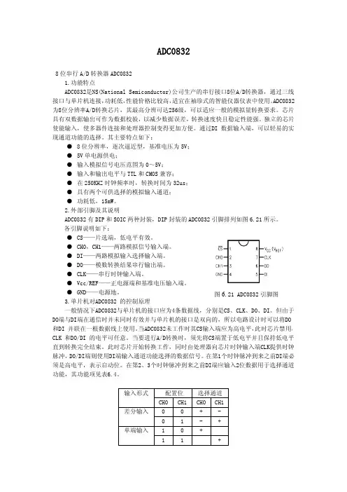
2.外部引脚及其说明ADC0832有DIP 和SOIC 两种封装,DIP 封装的ADC0832引脚排列如图6.21所示。
各引脚说明如下:●CS——片选端,低电平有效。
●CH0,CH1——两路模拟信号输入端。
●DI——两路模拟输入选择输入端。
●DO——模数转换结果串行输出端。
●CLK——串行时钟输入端。
●Vcc/REF——正电源端和基准电压输入端。
●GND——电源地。
3.单片机对ADC0832的控制原理一般情况下ADC0832与单片机的接口应为4条数据线,分别是CS、CLK、DO、DI。
但由于DO端与DI端在通信时并未同时有效并与单片机的接口是双向的,所以电路设计时可以将DO 和DI 并联在一根数据线上使用。
当ADC0832未工作时其CS输入端应为高电平,此时芯片禁用,CLK 和DO/DI 的电平可任意。
当要进行A/D转换时,须先将CS端置于低电平并且保持低电平直到转换完全结束。
此时芯片开始转换工作,同时由处理器向芯片时钟输入端CLK提供时钟脉冲,DO/DI端则使用DI端输入通道功能选择的数据信号。
ADC0832课程设计
ADC0832课程设计一、教学目标本课程的教学目标是使学生掌握ADC0832芯片的基本原理、功能、应用及其编程方法。
通过本课程的学习,学生将能够:1.描述ADC0832芯片的结构、工作原理和性能特点;2.理解ADC0832在不同领域的应用,如模拟信号处理、数据采集等;3.掌握ADC0832的编程方法,包括初始化、数据采集、数据转换等;4.能够运用ADC0832芯片解决实际问题,如设计简单的数据采集系统。
二、教学内容本课程的教学内容主要包括以下几个部分:1.ADC0832芯片的基本原理:介绍ADC0832的结构、工作原理和性能特点,使学生了解其在电路设计中的应用背景;2.ADC0832的功能与应用:讲解ADC0832的各个引脚功能、工作模式,并通过实例分析其在不同领域的应用,如模拟信号处理、数据采集等;3.ADC0832的编程方法:详细介绍ADC0832的编程步骤、初始化过程以及数据采集、转换的方法,让学生能够熟练操作ADC0832芯片;4.实践项目:安排适量的实践项目,让学生动手设计并实现基于ADC0832的数据采集系统,巩固所学知识。
三、教学方法为了提高教学效果,本课程将采用多种教学方法相结合的方式,包括:1.讲授法:讲解ADC0832的基本原理、功能、应用和编程方法,使学生掌握课程的基本知识;2.案例分析法:通过分析实际案例,使学生更好地理解ADC0832的应用场景和编程技巧;3.实验法:安排实践项目,让学生动手操作ADC0832芯片,培养学生的实际动手能力;4.讨论法:学生进行小组讨论,分享学习心得和经验,提高学生的合作能力和沟通能力。
四、教学资源为了支持本课程的教学,我们将准备以下教学资源:1.教材:选用国内权威出版的ADC0832相关教材,作为学生学习的主要参考资料;2.参考书:推荐学生阅读一些与ADC0832相关的书籍,以拓宽知识面;3.多媒体资料:制作PPT、教学视频等多媒体资料,辅助学生更好地理解课程内容;4.实验设备:准备ADC0832芯片、开发板等实验设备,为学生提供动手实践的机会。
单片机对adc0832的控制原理
单片机对adc0832的控制原理一、概述ADC0832是一种8位分辨率的单通道模数转换器,采用双重积分架构,可以将模拟信号转换为数字信号。
单片机可以通过控制ADC0832实现对模拟信号的采集和转换。
二、ADC0832的工作原理1. 双重积分架构ADC0832采用双重积分架构,将输入信号与一个内部参考电压进行比较,然后通过积分电路将输出结果逐渐趋近于输入信号。
当输出结果等于输入信号时,积分器停止计数,并将计数值输出为数字信号。
2. 工作模式ADC0832有两种工作模式:单次转换模式和自动转换模式。
单次转换模式下,每次启动一个新的转换需要发送启动命令;自动转换模式下,芯片会不断地进行转换并输出结果。
3. 时序控制在进行AD转换时,需要按照一定的时序进行控制。
具体来说,需要先将片选信号拉低使能芯片,在ADCS引脚上提供时钟脉冲,在START引脚上提供启动命令,在EOC引脚上读取结果并结束本次转换。
4. 数据格式ADC0832输出的数字信号是8位的,采用两个字节进行传输。
其中高字节的最高位为0,低7位存储转换结果;低字节的最高两位为0,低6位存储转换结果。
三、单片机对ADC0832的控制1. 硬件连接将ADC0832的引脚与单片机的引脚相连接,其中需要注意ADC0832的VCC和GND引脚需要与单片机提供的电源相连。
2. 软件编程单片机需要通过软件控制ADC0832进行AD转换。
具体来说,需要按照以下步骤进行编程:(1)初始化:设置ADC0832所连接的端口为输入端口,并设置相应引脚状态。
(2)启动转换:向START引脚发送启动命令,在ADCS引脚上提供时钟脉冲。
(3)等待转换结束:在EOC引脚上等待转换结束,并读取结果。
(4)输出结果:将读取到的结果进行处理并输出。
3. 注意事项在使用单片机控制ADC0832时,需要注意以下事项:(1)时序控制必须准确无误,否则会导致AD转换失败或者出现误差。
(2)电源稳定性对AD转换精度有很大影响,因此需要保证电源质量良好。
adc0832内部工作原理
adc0832内部工作原理一、引言ADC0832是一种8位分辨率的模数转换器,它可以将模拟信号转换为数字信号。
在本文中,我们将详细讨论ADC0832的内部工作原理。
二、基本概念在开始讨论ADC0832的内部工作原理之前,我们需要了解一些基本概念:1. 模拟信号:指连续变化的物理量所组成的信号。
2. 数字信号:指由离散数值表示的信号。
3. 分辨率:指数字转换器可以将模拟信号分成多少个等级。
4. 采样率:指数字转换器每秒钟可以采样多少次。
5. 时钟频率:指数字转换器内部时钟的频率。
三、ADC0832的基本结构ADC0832由以下几个主要部分组成:1. 输入缓冲区输入缓冲区用于保护输入电路不受外界干扰,并提供稳定的输入电压。
它通常由一个差分放大器和一个低通滤波器组成。
差分放大器用于放大差模输入电压,低通滤波器用于去除高频噪声。
2. 参考电压源参考电压源提供一个固定的参考电压,用于将模拟信号转换为数字信号。
它通常由一个精密的电压源和一个放大器组成。
3. 比较器比较器用于将输入信号与参考电压进行比较,并产生一个数字输出。
它通常由一个差分放大器和一个阈值电路组成。
差分放大器用于放大差模输入电压,阈值电路用于产生比较阈值。
4. 采样保持电路采样保持电路用于在ADC0832进行转换之前,将输入信号进行采样并保持其值不变。
它通常由一个开关和一个采样保持电容组成。
5. 计数器计数器用于控制ADC0832的转换速率,并计算转换结果。
它通常由一个时钟发生器和一个二进制计数器组成。
6. 数字输出接口数字输出接口用于将数字信号输出到外部系统。
它通常由一组并行输出引脚或串行输出引脚组成。
四、ADC0832的工作原理ADC0832的工作原理可以分为以下几个步骤:1. 输入缓冲区当模拟信号进入ADC0832时,首先经过输入缓冲区进行处理。
输入缓冲区通过差分放大器将差模输入电压放大,并通过低通滤波器去除高频噪声。
然后,输入缓冲区将处理后的信号送入采样保持电路。
ADC0832
ADC0832ADC08328位串⾏A/D 转换器ADC08321.功能特点ADC0832是NS(National Semiconductor)公司⽣产的串⾏接⼝8位A/D转换器,通过三线接⼝与单⽚机连接,功耗低,性能价格⽐较⾼,适宜在袖珍式的智能仪器仪表中使⽤。
ADC0832为8位分辨率A/D转换芯⽚,其最⾼分辨可达256级,可以适应⼀般的模拟量转换要求。
芯⽚具有双数据输出可作为数据校验,以减少数据误差,转换速度快且稳定性能强。
独⽴的芯⽚使能输⼊,使多器件连接和处理器控制变得更加⽅便。
通过DI 数据输⼊端,可以轻易的实现通道功能的选择。
其主要特点如下:●8位分辨率,逐次逼近型,基准电压为5V;●5V 单电源供电;●输⼊模拟信号电压范围为0~5V;●输⼊和输出电平与TTL 和CMOS 兼容;●在250KHZ 时钟频率时,转换时间为32us;●具有两个可供选择的模拟输⼊通道;●功耗低,15mW。
2.外部引脚及其说明ADC0832有DIP 和SOIC 两种封装,DIP 封装的ADC0832引脚排列如图6.21所⽰。
各引脚说明如下:●CS——⽚选端,低电平有效。
●CH0,CH1——两路模拟信号输⼊端。
●DI——两路模拟输⼊选择输⼊端。
●DO——模数转换结果串⾏输出端。
●CLK ——串⾏时钟输⼊端。
●Vcc/REF——正电源端和基准电压输⼊端。
●GND——电源地。
3.单⽚机对ADC0832的控制原理⼀般情况下ADC0832与单⽚机的接⼝应为4条数据线,分别是CS、CLK、DO、DI。
但由于DO端与DI端在通信时并未同时有效并与单⽚机的接⼝是双向的,所以电路设计时可以将DO 和DI 并联在⼀根数据线上使⽤。
当ADC0832未⼯作时其CS输⼊端应为⾼电平,此时芯⽚禁⽤,CLK 和DO/DI 的电平可任意。
当要进⾏A/D转换时,须先将CS端置于低电平并且保持低电平直到转换完全结束。
此时芯⽚开始转换⼯作,同时由处理器向芯⽚时钟输⼊端CLK提供时钟脉冲,DO/DI端则使⽤DI端输⼊通道功能选择的数据信号。
adc0832内部工作原理
adc0832内部工作原理1. 简介在嵌入式系统中,ADC(Analog-to-Digital Converter)是一种常见的模数转换器。
adc0832是一款典型的8位模数转换器,用于将模拟信号转换为数字信号。
本文将详细探讨adc0832的内部工作原理。
2. adc0832的构成adc0832由多个模块构成,包括输入电压电平比较器、采样保持电路、逐次逼近注册器(SAR)和数字信号输出缓冲器等。
2.1 输入电压电平比较器输入电压电平比较器用于将模拟信号与参考电压进行比较。
adc0832有两个模拟信号输入引脚,分别是AIN0和AIN1,以便进行差分输入。
输入的模拟信号经过放大和比较后,输出高低电平。
2.2 采样保持电路adc0832的采样保持电路用于将输入信号进行采样和保持。
在采样期间,输入信号的电压被保持在一个电容器上,以便在转换过程中保持稳定。
2.3 逐次逼近注册器(SAR)逐次逼近注册器(SAR)是adc0832的核心部分。
它通过逐位逼近的方式将模拟信号转换为数字信号。
工作原理如下:1.SAR从最高有效位(MSB)开始,将比较结果与DAC(Digital-to-AnalogConverter)输出进行比较。
2.如果比较结果大于DAC输出,则该位设置为1,否则设置为0。
3.SAR切换到下一位,重复上述过程。
4.直到所有位都被处理完毕,转换完成。
2.4 数字信号输出缓冲器数字信号输出缓冲器用于将数字信号进行缓冲,以便输出给外部设备。
3. adc0832的工作流程adc0832的工作流程如下:1.初始化:设置adc0832的工作模式、参考电压和输入信号源等。
2.转换开始信号:通过向adc0832发送一个转换开始信号,启动转换过程。
3.采样与保持:adc0832对输入信号进行采样并保持。
4.逐次逼近转换:adc0832通过逐位逼近的方式进行模拟信号转换,将其转换为数字信号。
5.转换完成信号:adc0832在转换完成后发送一个转换完成信号。