OB3393SCPA规格书 Datasheet
MCZ33937AEK;MCZ33937AEKR2;MCZ33937EK;MCZ33937EKR2;中文规格书,Datasheet资料
Figure 3. 33937A Pin Connections Table 1. 33937A Pin Definitions A functional description of each pin can be found in the Functional Pin Description section beginning on page 20.
Freescale Semiconductor Advance Information
Document Number: MC33937 Rev. 8.0, 8/2012
Three Phase Field Effect Transistor Pre-driver
The 33937A is a field effect transistor (FET) pre-drivers designed for three phase motor control and similar applications. The integrated circuit (IC) uses SMARTMOS technology. The IC contains three high side FET pre-drivers and three low side FET pre-drivers. Three external bootstrap capacitors provide gate charge to the high side FETs. The IC interfaces to a MCU via six direct input control signals, an SPI port for device setup and asynchronous reset, enable and interrupt signals. Both 5.0 and 3.0 V logic level inputs are accepted and 5.0 V logic level outputs are provided. Features • Fully specified from 8.0 to 40 V covers 12 and 24 V automotive systems • Extended operating range from 6.0 to 58 V covers 12 and 42 V systems • Greater than 1.0 A gate drive capability with protection • Protection against reverse charge injection from CGD and CGS of external FETs • Includes a charge pump to support full FET drive at low battery voltages • Dead time is programmable via the SPI port • Simultaneous output capability enabled via safe SPI command
ob6683cgpa规格书

ob6683cgpa规格书英文回答:OB6683CGPA Specification.Introduction:The OB6683CGPA specification outlines the requirements and standards for the OB6683CGPA product. Thisspecification aims to provide a detailed description of the product's features, functionality, and performance expectations. In this response, I will discuss the key aspects of the OB6683CGPA specification and provide examples to illustrate its application.Product Features:The OB6683CGPA is a versatile and high-performance device that offers a range of features to meet the needs of users. It is equipped with advanced technology andinnovative design elements. Some of its notable features include:1. High-resolution display: The OB6683CGPA boasts a vibrant and sharp display, allowing users to enjoy crystal-clear visuals and an immersive viewing experience.2. Powerful processor: With a state-of-the-art processor, the OB6683CGPA delivers lightning-fast performance, enabling seamless multitasking and smooth operation of resource-intensive applications.3. Extensive storage capacity: The OB6683CGPA offers ample storage space, allowing users to store a large amount of data, including photos, videos, and documents, without worrying about running out of space.4. Advanced camera system: The OB6683CGPA is equipped with a high-quality camera system, enabling users to capture stunning photos and videos with exceptional clarity and detail.Performance Expectations:The OB6683CGPA is designed to deliver exceptional performance across various tasks and applications. Its powerful hardware and optimized software ensure smooth and efficient operation. Some performance expectations for the OB6683CGPA include:1. Fast and responsive user interface: The OB6683CGPA provides a seamless user experience with its quick and responsive interface. Users can navigate through menus, open applications, and perform tasks without any lag or delay.2. Smooth gaming experience: The OB6683CGPA is capable of handling graphically demanding games with ease. Users can enjoy a smooth and immersive gaming experience without experiencing any frame drops or stuttering.3. Efficient multitasking: The OB6683CGPA allows users to run multiple applications simultaneously without compromising performance. Users can switch between appsseamlessly and enjoy a seamless multitasking experience.4. Long battery life: The OB6683CGPA is equipped with a high-capacity battery that provides extended usage time. Users can enjoy using the device for extended periodswithout worrying about frequent recharging.中文回答:OB6683CGPA规格书。
OB3Z12A规格书

Product ListOB3Z12ADescriptionThe OB3Z12A is a LED lighting controller. It has hardware dimming mechanism supporting up to 3-channel dimming control. The control interfaces include Liner DC, VR, Key/Button, PWM duty and IR, various digital and analog diming control methods. The OB3Z12A equips with serial communication interfaces for inter-connection to host or remote controllers. The on-chip non-volatile memory contains the system preset parameters and configurations.Features●Operating V oltage: 4.5V ~ 5.5V●3-ch PWM dimming control output● 1 analog VR dimming control input● 1 analog DC-in dimming control input● 1 digital PWM duty dimming control input● 1 digital IR remote dimming control input●Serial interfaces: UART, I2C.●Package type: 8-SOP.Pin Configuration8-SOPPin DescriptionPin Symbol I/O Description1 RX/AN0 I VR, analog diming control input. Serial Receiver Input2 TX/AN1 I/O Liner analog diming control input. Serial Transmitter Output3 DIM3 O PWM dimming output ch-34 DIM2 O PWM dimming output ch-25 VSS I Power supply6 SDA/IR I/O I2C Data. IR input7 DIM1/SCL/Duty I/O I2C Clock. PWM dimming output ch-1. Duty dimming control input8 VDD I Power SupplyOperating ConditionsSymbol Description Min. Typ. Max. Unit. RemarksTA Operating temperature -40 25 85 ℃Ambient temperature under bias VDD Supply voltage 4.5 5.5 VDC CharacteristicsT A = -40℃ to 85℃, V dd= 5.0VSymbol Parameter Valid Min Max Units ConditionsVIL1Input Low-voltage DIMx,SDA,SCL,Tx,Rx-0.5 0.8 V Vdd=5VVIH1Input High-voltage DIMx,SDA,SCL,Tx,Rx2.0 V CC + 0.5 VVOL Output Low-voltage DIMx,SDA,SCL,Tx,Rx0.4 V IOL=4.9mAVOH1Output High-voltageusing Strong Pull-upDIMx,SDA,SCL,Tx,Rx90% V CC V IOH= -4.6mA2.4 V IOH= -14mAVOH2Output High-voltageusing Weak Pull-upDIMx,SDA,SCL,Tx,Rx2.4 V IOH= -250uAIIL Logic 0 Input Current DIMx,SDA,SCL,Tx,Rx-75 uA Vin= 0.45VITL Logical TransitionCurrentDIMx,SDA,SCL,Tx,Rx-650 uA Vin= 2.0VILI Input Leakage Current DIMx,SDA,SCL,Tx,Rx±10 uA 0.45V<Vin<VccICC Power Supply Current VDD 5 mA Vdd =5V 25 ℃。
OB3398 Datasheet_铱宝_150602
O
nB
On chip Over temperature Section T_otp T_otp_rec 135 120 ℃ ℃
Note:
1. Freq_Max indicates IC internal maximum clock frequency. In system application, the maximum operation frequency of 103KHz nominal occurs at maximum output power or the transition point from CV to CC.
tia
Ordering Information Part Number Description OB3398MP SOT23-5, Pb-free,T&R
ratings” may cause permanent damage to the device. These are stress ratings only, functional operation of the device at these or any other conditions beyond those indicated under “recommended operating conditions” is not implied. Exposure to absolute maximum-rated conditions for extended periods may affect device reliability.
V_clamping T_r T_f
Output clamp voltage Output rising time 1V~ 9V@ CL=500pF Output falling time 9V~1V@ CL=500pF Over temperature protection trigger point Over temperature protection recovery point
欧姆伯特电子 3R3型号电感说明书

Dimensions: [mm]Scale - 5:1Product Marking:Marking3R3 (Inductance Code)7440404203374404042033BC74404042033T e m p e r a t u r eT pT L74404042033Cautions and Warnings:The following conditions apply to all goods within the product series of WE-LQS of Würth Elektronik eiSos GmbH & Co. KG:General:•This electronic component is designed and manufactured for use in general electronic equipment.•Würth Elektronik must be asked for written approval (following the PPAP procedure) before incorporating the components into any equipment in fields such as military, aerospace, aviation, nuclear control, submarine, transportation (automotive control, train control, ship control), transportation signal, disaster prevention, medical, public information network etc. where higher safety and reliability are especially required and/or if there is the possibility of direct damage or human injury.•Electronic components that will be used in safety-critical or high-reliability applications, should be pre-evaluated by the customer. •The component is designed and manufactured to be used within the datasheet specified values. If the usage and operation conditions specified in the datasheet are not met, the wire insulation may be damaged or dissolved.•Do not drop or impact the components, the component may be damaged.•Würth Elektronik products are qualified according to international standards, which are listed in each product reliability report. Würth Elektronik does not warrant any customer qualified product characteristics beyond Würth Elektroniks’ specifications, for its validity and sustainability over time.•The responsibility for the applicability of the customer specific products and use in a particular customer design is always within the authority of the customer. All technical specifications for standard products also apply to customer specific products.Product specific:Soldering:•The solder profile must comply with the technical product specifications. All other profiles will void the warranty.•All other soldering methods are at the customers’ own risk.•Strong forces which may affect the coplanarity of the components’ electrical connection with the PCB (i.e. pins), can damage the part, resulting in avoid of the warranty.Cleaning and Washing:•Washing agents used during the production to clean the customer application might damage or change the characteristics of the wire insulation, marking or plating. Washing agents may have a negative effect on the long-term functionality of the product.•Using a brush during the cleaning process may break the wire due to its small diameter. Therefore, we do not recommend using a brush during the PCB cleaning process.Potting:•If the product is potted in the customer application, the potting material may shrink or expand during and after hardening. Shrinking could lead to an incomplete seal, allowing contaminants into the core. Expansion could damage the components. We recommend a manual inspection after potting to avoid these effects.Storage Conditions:• A storage of Würth Elektronik products for longer than 12 months is not recommended. Within other effects, the terminals may suffer degradation, resulting in bad solderability. Therefore, all products shall be used within the period of 12 months based on the day of shipment.•Do not expose the components to direct sunlight.•The storage conditions in the original packaging are defined according to DIN EN 61760-2.•The storage conditions stated in the original packaging apply to the storage time and not to the transportation time of the components. Packaging:•The packaging specifications apply only to purchase orders comprising whole packaging units. If the ordered quantity exceeds or is lower than the specified packaging unit, packaging in accordance with the packaging specifications cannot be ensured. Handling:•Violation of the technical product specifications such as exceeding the nominal rated current will void the warranty.•Applying currents with audio-frequency signals may result in audible noise due to the magnetostrictive material properties.•The temperature rise of the component must be taken into consideration. The operating temperature is comprised of ambient temperature and temperature rise of the component.The operating temperature of the component shall not exceed the maximum temperature specified.These cautions and warnings comply with the state of the scientific and technical knowledge and are believed to be accurate and reliable.However, no responsibility is assumed for inaccuracies or incompleteness.Würth Elektronik eiSos GmbH & Co. KGEMC & Inductive SolutionsMax-Eyth-Str. 174638 WaldenburgGermanyCHECKED REVISION DATE (YYYY-MM-DD)GENERAL TOLERANCE PROJECTIONMETHODChriB001.0072023-02-28DIN ISO 2768-1mDESCRIPTIONWE-LQS SMT Semi-ShieldedPower Inductor ORDER CODE74404042033SIZE/TYPE BUSINESS UNIT STATUS PAGEImportant NotesThe following conditions apply to all goods within the product range of Würth Elektronik eiSos GmbH & Co. KG:1. General Customer ResponsibilitySome goods within the product range of Würth Elektronik eiSos GmbH & Co. KG contain statements regarding general suitability for certain application areas. These statements about suitability are based on our knowledge and experience of typical requirements concerning the areas, serve as general guidance and cannot be estimated as binding statements about the suitability for a customer application. The responsibility for the applicability and use in a particular customer design is always solely within the authority of the customer. Due to this fact it is up to the customer to evaluate, where appropriate to investigate and decide whether the device with the specific product characteristics described in the product specification is valid and suitable for the respective customer application or not.2. Customer Responsibility related to Specific, in particular Safety-Relevant ApplicationsIt has to be clearly pointed out that the possibility of a malfunction of electronic components or failure before the end of the usual lifetime cannot be completely eliminated in the current state of the art, even if the products are operated within the range of the specifications.In certain customer applications requiring a very high level of safety and especially in customer applications in which the malfunction or failure of an electronic component could endanger human life or health it must be ensured by most advanced technological aid of suitable design of the customer application that no injury or damage is caused to third parties in the event of malfunction or failure of an electronic component. Therefore, customer is cautioned to verify that data sheets are current before placing orders. The current data sheets can be downloaded at .3. Best Care and AttentionAny product-specific notes, cautions and warnings must be strictly observed. Any disregard will result in the loss of warranty.4. Customer Support for Product SpecificationsSome products within the product range may contain substances which are subject to restrictions in certain jurisdictions in order to serve specific technical requirements. Necessary information is available on request. In this case the field sales engineer or the internal sales person in charge should be contacted who will be happy to support in this matter.5. Product R&DDue to constant product improvement product specifications may change from time to time. As a standard reporting procedure of the Product Change Notification (PCN) according to the JEDEC-Standard inform about minor and major changes. In case of further queries regarding the PCN, the field sales engineer or the internal sales person in charge should be contacted. The basic responsibility of the customer as per Section 1 and 2 remains unaffected.6. Product Life CycleDue to technical progress and economical evaluation we also reserve the right to discontinue production and delivery of products. As a standard reporting procedure of the Product Termination Notification (PTN) according to the JEDEC-Standard we will inform at an early stage about inevitable product discontinuance. According to this we cannot guarantee that all products within our product range will always be available. Therefore it needs to be verified with the field sales engineer or the internal sales person in charge about the current product availability expectancy before or when the product for application design-in disposal is considered. The approach named above does not apply in the case of individual agreements deviating from the foregoing for customer-specific products.7. Property RightsAll the rights for contractual products produced by Würth Elektronik eiSos GmbH & Co. KG on the basis of ideas, development contracts as well as models or templates that are subject to copyright, patent or commercial protection supplied to the customer will remain with Würth Elektronik eiSos GmbH & Co. KG. Würth Elektronik eiSos GmbH & Co. KG does not warrant or represent that any license, either expressed or implied, is granted under any patent right, copyright, mask work right, or other intellectual property right relating to any combination, application, or process in which Würth Elektronik eiSos GmbH & Co. KG components or services are used.8. General Terms and ConditionsUnless otherwise agreed in individual contracts, all orders are subject to the current version of the “General Terms and Conditions of Würth Elektronik eiSos Group”, last version available at .Würth Elektronik eiSos GmbH & Co. KGEMC & Inductive SolutionsMax-Eyth-Str. 174638 WaldenburgGermanyCHECKED REVISION DATE (YYYY-MM-DD)GENERAL TOLERANCE PROJECTIONMETHODChriB001.0072023-02-28DIN ISO 2768-1mDESCRIPTIONWE-LQS SMT Semi-ShieldedPower Inductor ORDER CODE74404042033SIZE/TYPE BUSINESS UNIT STATUS PAGE。
DC339-A -B低压差稳压器数据手册说明书

12REFERENCEDESIGNATOR QUANTITY PART NUMBER DESCRIPTION VENDOR TELEPHONE ADJ10Optional ResistorC110603ZG105ZAT1A1µF 10V Y5V Chip Capacitor AVX(843) 946-0362 C210402ZG104ZAT1A0.1µF 10V Y5V Chip Capacitor AVX(843) 946-0362 C31LMK325BJ106MN10µF 10V X7R Chip Capacitor Taiyo-Yuden(408) 573-4150 E1 to E442308-2Pad Turret Mill-Max(516) 922-6000 JP10Optional JumperJP216351-12G1Connector, SMT2X6, 0.39" Gap Comm-Con(626) 301-4200 Shunts for2CTAIJ1MM-G Shunts for 0.39" Gap Comm-Con(626) 301-4200 JP1 and JP2R11CR05-2613FM261k 1/16W 1% Chip Resistor AAC(800) 508-1521 R21CR05-3653FM365k 1/16W 1% Chip Resistor AAC(800) 508-1521 R31CR05-4223FM422k 1/16W 1% Chip Resistor AAC(800) 508-1521 R41CR05-7683FM768k 1/16W 1% Chip Resistor AAC(714) 255-9186 R51CR05-2493FM249k 1/16W 1% Chip Resistor AAC(714) 255-9186 U11LT1762EMS8 or8-Lead MSOP IC Version -A LTC(408) 432-1900 LT1962EMS88-Lead MSOP IC Version -BPARTS LISTOPERATIOUHOOK-UPSolid turret terminals are provided for easy connection to supplies and test equipment. Connect a 0V to 20V, 0.5A power supply across the IN and GND terminals and the load across the OUT and GND terminals. The SHDN pin can be disconnected from IN via JP1 to allow for separate shutdown control via a secondary control line. JP2 can be used to select any of a number of common fixed output voltages, or used in conjunction with ADJ1 to create a custom output voltage using the formula:ADJ1 = (V OUT – 1.22V)/4.93µAOUTPUT CAPACITOR SELECTIONThe output capacitor C3 is a 10µF X7R ceramic chip capacitor. Should a different output capacitor be desired, care must be exercised with the selection. Many ceramic capacitor dielectrics exhibit strong temperature and voltage characteristics that reduce their effective capaci-tance to as low as 10% to 20% of nominal over the full range. For further information, see Linear Technology Application Note 83, “Performance Verification of Low Noise, Low Dropout Regulators,” Appendix␣B, “Capaci-tor Selection Considerations,” reprinted below.CAPACITOR SELECTION CONSIDERATIONSBypass Capacitance and Low Noise Performance Adding a capacitor between the regulator’s V OUT and BYP pins lowers output noise. A good quality, low leakage capacitor is recommended. This capacitor bypasses the regulator’s reference, providing a low frequency noise pole. A 0.01µF capacitor lowers the output voltage noise to 20µV RMS. Using a bypass capacitor also improves transient response. With no bypassing and a 10µF output capacitor, a 10mA to 500mA load step settles within 1% of final value in under 100µs. With a 0.01µF bypass capacitor, the output settles within 1% for the same load step in under 10µs; total output deviation is inside 2.5%. Regulator start-up time is inversely proportional to bypass capacitor size, slowing to 15ms with a 0.01µF bypass capacitor and 10µF at the output.34567Information furnished by Linear Technology Corporation is believed to be accurate and reliable.However, no responsibility is assumed for its use. Linear Technology Corporation makes no represen-tation that the interconnection of its circuits as described herein will not infringe on existing patent rights.8dc339 LT/TP 0301 500 • PRINTED IN USA© LINEAR TECHNOLOGY CORPORA TION 2001Linear Technology Corporation1630 McCarthy Blvd., Milpitas, CA 95035-7417(408) 432-1900 q FAX: (408) 434-0507 q 。
OB3392 Datasheet
o
富
260 ℃
Absolute Maximum Ratings Parameter VDD Voltage GATE Voltage CS Input Voltage FB Input Voltage CMP Input Voltage Min/Max Operating Junction Temperature TJ Min/Max Storage Temperature Tstg Lead Temperature (Soldering, 10secs)
Value -0.3 to 35V -0.3 to 10V -0.3 to 7V -0.3 to 7V -0.3 to 7V
-55 to 150 ℃
Preliminary Datasheet OB_DOC_DS_339200
华
-40 to 150 ℃
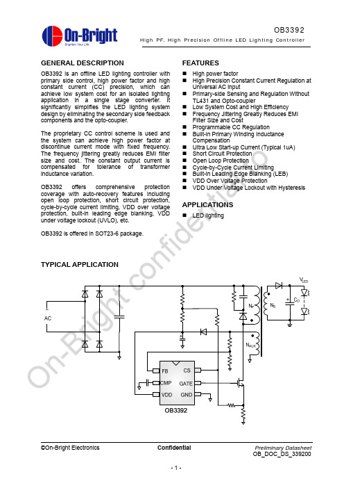
OB3392
High PF, High Precision Offline LED Lighting Controller
TYPICAL APPLICATION
O
n-
©On-Bright Electronics
Br ig
ht
co
nf
id
Confidential -1-
en t
LED lighting
APPLICATIONS
ia
lt
o
富
Preliminary Datasheet OB_DOC_DS_339200
华
OB3392
ELECTRICAL CHARACTERISTICS
(TA = 25℃, VDD=15V, if not otherwise noted) Symbol Parameter Supply Voltage (VDD) Section I start-up I op UVLO(OFF) UVLO(ON) VDD_OVP TLEB Vth_ocp Vout_ovp Start-up Current Operation Current VDD Under Voltage Lockout Exit VDD Under Voltage Lockout Enter VDD Over Voltage Protection LEB Time Over Current Threshold Output Over Voltage Protection 19 8 27 VDD=20V 1 1.3 21 9 30 3 2.0 23 uA mA Test Conditions Min Typ Max Unit
OB3Z12A规格书
Product ListOB3Z12ADescriptionThe OB3Z12A is a LED lighting controller. It has hardware dimming mechanism supporting up to 3-channel dimming control. The control interfaces include Liner DC, VR, Key/Button, PWM duty and IR, various digital and analog diming control methods. The OB3Z12A equips with serial communication interfaces for inter-connection to host or remote controllers. The on-chip non-volatile memory contains the system preset parameters and configurations.Features●Operating V oltage: 4.5V ~ 5.5V●3-ch PWM dimming control output● 1 analog VR dimming control input● 1 analog DC-in dimming control input● 1 digital PWM duty dimming control input● 1 digital IR remote dimming control input●Serial interfaces: UART, I2C.●Package type: 8-SOP.Pin Configuration8-SOPPin DescriptionPin Symbol I/O Description1 RX/AN0 I VR, analog diming control input. Serial Receiver Input2 TX/AN1 I/O Liner analog diming control input. Serial Transmitter Output3 DIM3 O PWM dimming output ch-34 DIM2 O PWM dimming output ch-25 VSS I Power supply6 SDA/IR I/O I2C Data. IR input7 DIM1/SCL/Duty I/O I2C Clock. PWM dimming output ch-1. Duty dimming control input8 VDD I Power SupplyOperating ConditionsSymbol Description Min. Typ. Max. Unit. RemarksTA Operating temperature -40 25 85 ℃Ambient temperature under bias VDD Supply voltage 4.5 5.5 VDC CharacteristicsT A = -40℃ to 85℃, V dd= 5.0VSymbol Parameter Valid Min Max Units ConditionsVIL1Input Low-voltage DIMx,SDA,SCL,Tx,Rx-0.5 0.8 V Vdd=5VVIH1Input High-voltage DIMx,SDA,SCL,Tx,Rx2.0 V CC + 0.5 VVOL Output Low-voltage DIMx,SDA,SCL,Tx,Rx0.4 V IOL=4.9mAVOH1Output High-voltageusing Strong Pull-upDIMx,SDA,SCL,Tx,Rx90% V CC V IOH= -4.6mA2.4 V IOH= -14mAVOH2Output High-voltageusing Weak Pull-upDIMx,SDA,SCL,Tx,Rx2.4 V IOH= -250uAIIL Logic 0 Input Current DIMx,SDA,SCL,Tx,Rx-75 uA Vin= 0.45VITL Logical TransitionCurrentDIMx,SDA,SCL,Tx,Rx-650 uA Vin= 2.0VILI Input Leakage Current DIMx,SDA,SCL,Tx,Rx±10 uA 0.45V<Vin<VccICC Power Supply Current VDD 5 mA Vdd =5V 25 ℃。
- 1、下载文档前请自行甄别文档内容的完整性,平台不提供额外的编辑、内容补充、找答案等附加服务。
- 2、"仅部分预览"的文档,不可在线预览部分如存在完整性等问题,可反馈申请退款(可完整预览的文档不适用该条件!)。
- 3、如文档侵犯您的权益,请联系客服反馈,我们会尽快为您处理(人工客服工作时间:9:00-18:30)。
保证声明 昂宝电子有限公司依从其标准保单书承诺,出售时所有硬件产品性能参数均符合产品的相应使用规格书。产
恒
OB3393S 提供一系列全面的可自动恢复保护,包 括 LED 开路保护、LED 短路保护、逐周期峰值电流
深 限制,VDD 过压保护、欠压保护和锁存的过温保护
等。
to OB3393S 提供 SOP-8 封装。
内置前沿消隐 (LEB) 完善的自恢复保护功能
LED 短路保护 LED 开路保护 VDD 欠压保护
8-Pin Plastic SOP
OB3393S
高精度原边反馈 LED 控制器
恒
ht Confidential to 深 Symbol ig A
A1
r A2
b
Bc -D
E
nE1 e
OL
Dimensions In Millimeters
Min
Max
1.350
1.750
0.050
0.250
1.250
1.650
I/O 描述 I 电流采样端
无连接,必须悬空
P 电源供电端 I 内部高压功率管源极 I 内部高压功率管漏极 P 无连接,必须悬空并且不要放置焊盘 P地
©On-Bright Electronics
Confidential 3
Preliminary Datasheet OB_DOC_DS_3393S00_CN
启动电流 工作电流 VDD 欠压保护(OFF)阈值 VDD 欠压保护(ON)阈值 VDD 钳位阈值
前沿消隐时间 恒流 OCP 阈值
Td_oc
芯片传输延迟
n Toff_max
最大 OFF 时间
e Toff_min
最小 OFF 时间
fid Ton_max
最大 ON 时间
源极驱动
n Rdson_l
源极驱动开关管导通阻抗
制技术,无需 TL431 和光耦等二次侧元器件;极低 高效率、低系统成本
的工作电流,无需辅助绕组供电和检测,芯片采用 可调节设定恒流输出特性
专利的恒流控制方式,实现高精度的 LED 恒流输出 特性。LED 电流可以通过调节外部 CS 引脚上的检 测电阻 Rs 来设定。
内置原边电感量补偿 内置线电压补偿 CC 内置逐周期峰值电流限制
0.310
0.510
0.100
0.250
4.700
5.150
3.800
4.000
5.800
6.200
1.270 (BSC)
0.400
1.270
Dimensions In Inches
Min
Max
0.053
0.069
0.002
0.010
0.049
0.065
0.012
0.020
0.004
0.010
0.185
OB3393S
高精度原边反馈 LED 控制器
概述
特性
OB3393S 是一款高精度、低成本的 LED 驱动控制 输入电压全范围实现高精度恒流输出特性
器,应用于反激隔离 LED 照明。
原边采样和调整,无需 TL431 和光耦
OB3393S 内部集成 650V 功率管,采用原边反馈控 极低的工作电流,无需辅助绕组供电和检测
Preliminary Datasheet OB_DOC_DS_3393S00_CN
OB3393S
高精度原边反馈 LED 控制器
基本信息
引脚排布 SOP-8 引脚图如下.
额定封装散热 封装 SOP-8
RθJA (℃/W) 150
.
CS
1
8 GND
应用极限参数 参数
规格
NC
2
7 GND
VDD 电压 DRAIN 电压
过温保护
l APPLICATIONS tia LED 照明
en 典型应用图
nfid ~
+
On-Bright Co AC
+
CS GND NC GND VDD Drain SW Drain
OB3393S
VLED
+ CO
NP
NS
©On-Bright Electronics
Confidential -1-
ZZZ:Lot Code
l C: SOP8 tia P:Pb-free Package
S:Character Code
n s: Internal Code(Optional)
fide 引脚说明
引脚号 1
n 2 o 3
4
C 5,6 t 7 On-Brigh 8
引脚说明 CS
NC
VDD SW DRAIN NC GND
Packing
Blank:Tube A: Tape/Reel
©On-Bright Electronics
Confidential -2-
Preliminary Datasheet OB_DOC_DS_3393S00_CN
标识信息
OB3393S
高精度原边反馈 LED 控制器
恒
深 Y: Year Code to WW: Week Code (01-52)
以确保客户产品及应用的风险降到最低。
to 医疗领域 l 昂宝电子有限公司的产品不可用于维持、延续人类生命等医疗设备,并对其产品被用于医疗领域所造成的任
何损害或索赔不承担任何法律责任。
tia 军用领域
昂宝电子有限公司的产品不可用于军用领域,并对其产品被用于军用领域所造成的任何损害或索赔不承担任
On-Bright Confiden 何法律责任。
CS 输入电压
-0.3 to 7V
SW 输入电压
-0.3 to 9V
最小/最大工作结温 TJ 最小/最大储藏温度 Tstg 管脚焊接温度(10secs)
-40 to 150 ℃ -55 to 150 ℃ 260 ℃
备注: 芯片的实际应用条件超出规定的“应用极限值”将会
对芯片造成永久性损伤。以上应用极限值标志了芯片可承
受应力等级,但并不建议芯片在此极限条件或超出“推荐工
作条件”下工作。芯片长时间处于最大额定工作条件,会影
响芯片的可靠性。
n OB3393S
X
X
X
On-Bright Confide High Precision Offline LED Power Switch
Package C:SOP8
Package Pb free P:Pb-free
恒 品的测试和其它质量管理技术可对此担保。除了某些政府要求的项目,没有必要对每个产品的所有参数进行
测试。 昂宝电子有限公司对产品应用方面的设计协助或客户产品的设计不具任何义务。客户产品中使用昂宝电子的
深 产品、性能规格书和使用说明书,客户应对自己的产品及应用负责。客户应提供适当的设计和操作保护措施,
o OTP Section
C OTP
过温保护温度
t Power MOSFET Section
BVdss
功率管漏极-源极击穿电压
On-Brigh Rds,on
功率管导通阻抗
VDD=UVLO(OFF)-1 VDD=7.5V
1mA
120 150 uA
160 320 uA
7
V
6
V
8
V
0.3
485 500
From OCP comparator to base drive
©On-Bright Electronics
Confidential -6-
Preliminary Datasheet OB_DOC_DS_3393S00_CN
恒 -0.3 to 18V
-0.3 to 650V
VDD 3
6 Drain
深 SW
4
5 Drain
to 定购信息
l 型号
描述
tia OB3393SCP
OB3393SCPA
8 Pin SOP, Pb free in Tube 8 Pin SOP, Pb free in T&R
备注: 如无特殊说明,器件提供的是无铅封装。
0.203
0.150
0.157
0.228
0.244
0.050 (BSC)
0.016
0.050
θ
0º
8º
0º
8º
©On-Bright Electronics
Confidential -5-
Preliminary Datasheet OB_DOC_DS_3393S00_CN
OB3393S
高精度原边反馈 LED 控制器
100
600
4.5 5
50
us 515 mV
ns
us 5.5 us
us
Static, Id=1A
1.3
ohm
150
℃
650
V
18
ohm
©On-Bright Electronics
Confidential -4-
Preliminary Datasheet OB_DOC_DS_3393S00_CN
封装结构信息
OB3393S
高精度原边反馈 LED 控制器
电气参数
(如无特殊说明,环境温度 TA = 25℃, VDD=7.5V)
符号
描述
测试条件
最 小 值
典 值