STM32_FLASH的3种烧写方式
STM32内部FLASH读写操作详解

STM32内部FLASH读写操作详解
在STM32中,FLASH存储器被分为多个扇区。
每个扇区的大小根据芯
片型号而定,可以是16KB、32KB、64KB等大小。
每个扇区又被分为若干
个页,每个页的大小为2KB、4KB、8KB等。
读取FLASH数据的操作相对简单,可以通过读取内存地址的方式来实现。
由于FLASH时序特殊,读取速度相对较慢,所以在使用FLASH存储数
据时需要考虑读取的效率。
写入FLASH数据时,需要注意以下几点:
1.写入数据必须按照页的大小进行,即每次写入的数据不能超过页的
大小。
2.写入数据时,必须将FLASH模块解锁,否则写入操作将被禁止。
写
入完成后,需要将FLASH模块重新锁定。
3.写入FLASH数据时,如果写入的数据与指定地址处的数据不相同,
会导致页擦除。
所以在写入之前,需要将指定地址处的数据保存下来,并
进行适当的处理。
4.写入FLASH数据后,需要等待写入操作完成,然后进行擦除操作。
擦除操作可以是扇区擦除或页擦除。
除了普通的读写操作,STM32内部FLASH还提供了一些高级的功能,
如扇区擦除、页擦除、半页擦除、字节擦除等。
这些功能可以根据实际需
求进行选择和应用。
总结起来,对于STM32内部FLASH的读写操作,需要注意解锁和锁定FLASH模块、按页写入数据、写入完整性的保证、擦除操作的执行等细节。
通过合理的使用这些操作,可以实现对STM32内部FLASH的有效管理和利用。
如何通过JLINK烧写STM32程序

百为技术有限公司
7、 此时打开要烧写到 STM32 的 hex 文件
打开后如下图示:
百为技术有限公司
8、 然后点击 Target->Program & Verify 进行烧写
9、 弹出如下界面表示完成烧写
百为技术有限公司
如何通过 JLINK 烧写 STM32 程序
1、 首先安装 JLINK 驱动,Setup_JLinkARM_V420p.exe
2、 从开始程序菜单打开 J-FLASH 程序, 所有程序->SEGGER->J-Link ARM V4.20p->J-Flash ARM
百为技术有限公司
3、 点击 Options->Project settings
百为技术有限公司
4、 弹出如下界面,进入 CPU 页面,选择 Device ST STM32F103ZE,点击确定
百为技术有限公司
5、 用 JLINK 连接开发板和 PC,点击 Target->Connet 进行连接。
百为技术有限ห้องสมุดไป่ตู้司
6、 连接完成后,可以看到类似如下信息: - J-Link found 2 JTAG devices. Core ID: 0x3BA00477 (Cortex-M3) - Connected successfully
STM32_FLASH的3种烧写方式
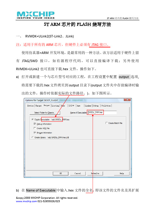
ST ARM 芯片的FLASH 烧写方法一、 RVMDK+ULink2(ST ‐Link2、JLink)注:适用于所有的ARM芯片,但硬件上必须有JTAG 接口。
使用仿真器+ARM 开发环境,是最常用的一种方法。
该方法适用于硬件上留有JTAG/SWD 接口,如有源程序代码,可以直接编译下载;另外使用RVMDK+ULink2也可直接下载.hex 文件,操作如下。
a) 打开或新建一个与芯片型号对应的工程,在工程设置中配置output 选项,将需要下载的.hex 文件拷贝到output 目录下(output 文件夹中存放编译时输),如下图所示。
©2008 MXCHIP Corporation. All rights reserved.b) 在Name of Executable:中输入.hex名,如上图所示。
c) 配置Utilities 选项,选中Use Target Driver for Flash Programming 项(默认情所示。
©2008 MXCHIP Corporation. All rights reserved.d) c)添加Flash Programming Algorithm ,即添加与目标芯片对应的Flash 编程算法,如下图所示。
e)以上步骤完成后,连接仿真器和目标板,即可把目标程序烧写到芯片的Flash中。
二、 串口+ISP软件注:适用于带有ISP功能的ARM芯片,需要硬件上留有COM接口,且芯片的启动模式可设置。
用户的ARM系列芯片带有ISP(在系统中编程)功能,则可使用其ISP功能,通过串口和ISP软件来下载.bin文件。
下面以STM32系列芯片为例(STM32全系列芯片都带有ISP功能),演示该烧写方法。
a)将USART1口连接到PC的COM口(通常ISP使用的UART口都是芯片的第一个UART口),设置芯片的启动模式为System Memary模式(BOOT1为0,©2008 MXCHIP Corporation. All rights reserved.BOOT0为1)。
STM32烧写程序步骤
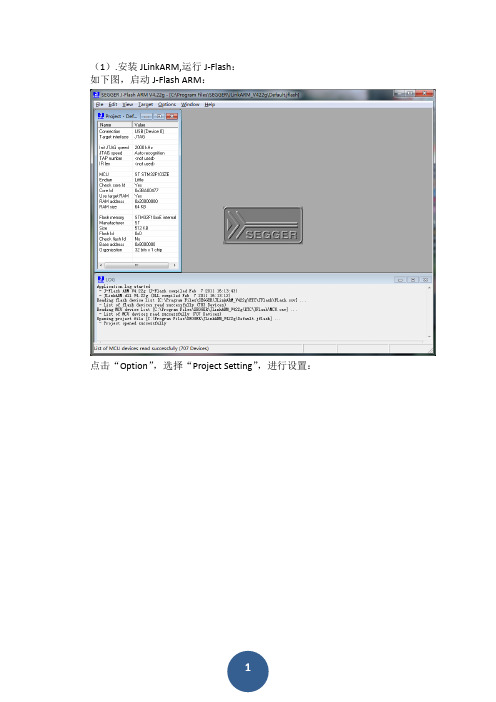
(1).安装JLinkARM,运行J-Flash:
如下图,启动J-Flash ARM:
点击“Option”,选择“Project Setting”,进行设置:
选择烧写方式为SWD:
选择CPU型号为STM32F103C8:
设置后会提示下图所示信息:
(2).连接目标板
将J-LINK一端通过USB线和PC连接起来,另一端按所给的接线图和JTAG口相连,接线图如下:
给工业节点提供12V电源,然后如下图所示点击“connect”:
连接成功后会提示下图所示信息:
(3).下载HEX文件
点击File下的open,打开Hex文件:
点击Target,选择Auto,将下载Hex到ARM:程序下载进度条显示如下:
下图为程序下载成功:
点击”确定”按钮,后按下F9按键,等待一会,程序将运行起来,在下图的状态栏提示如下字符串才能说明程序真正烧进去:
- Target application started。
单片机程序烧录的3种方式(ISP、ICP、IAP)是什么

单片机程序烧录的3种方式(ISP、ICP、IAP)是什么说起给单片机烧录程序,大家应该都不陌生吧,我最早接触单片机是从51单片机开始的,型号是STC89C52RC,当时烧录程序就是用的下面这种烧录软件——STC-ISP。
这种方式,通过串口连接单片机,选择一个合适的波特率就可以烧录了。
后来学习STM32,编程时使用KEIL软件自带的下载按钮就能下载程序,方便了不少,但需要额外使用J-Link等下载器。
再后来,接触到产品研发,给已经发布出的产品升级,都是要靠远程无线升级的(想想看,产品已经到客户那里了,当软件需要升级时,要是还使用有线的方式烧录程序,得有多麻烦)既然给单片机烧录程序的方式有多种,那烧录方式具体怎么分类呢?可以分为3种:ISP(In-System Programming)在系统编程,使用引导程序(Bootloader)加上外围UART/SPI等接口进行烧录。
ICP (In-circuit programmer)在电路编程,使用SWD/JTAG接口。
IAP(In-Application Programming)指MCU可以在系统中获取新代码并对自己重新编程,即用程序来改变程序。
这3种烧录方式的原理是什么呢?在分析原理之前,需要先了解一下单片机Flash的访问地址,看看程序是烧录到哪个位置了。
单片机Flash在地址映射表中位置下图是一张STM32F4xx的地址映射表,从0x0000 0000到0xFFFF FFFF,总计4Gbyte。
单片机的片上Flash、片上RAM、片上外设以及外部扩展接口的访问地址,都被映射到这4Gbyte的范围之内。
这张图中,我们需要先注意下半部分Main memory 主存储区通常,我们编写的代码,是放到主存储区的起始位置(0x0800 0000)开始运行的,烧录程序时,直接将程序烧录到这里即可(KEIL 软件给STM32烧录程序的默认烧写地址就是0x0800 0000开始)System memory系统存储区System memory(起始位置0x1FFF 000)是STM32在出厂时,由ST在这个区域内部预置了一段BootLoader,也就是我们常说的ISP程序,这是一块ROM,出厂后无法修改。
单片机片内存储器如何烧写几种烧写方式介绍

单片机片内存储器如何烧写几种烧写方式介绍单片机片内存储器烧写是将程序代码或数据写入单片机的内部存储器中的过程。
单片机的内部存储器包括闪存、EEPROM、RAM等。
这些存储器可以通过不同的烧写方式进行烧写。
下面将介绍几种常见的单片机片内存储器烧写方式。
1.并行编程方式并行编程方式是最早出现的一种单片机烧写方式。
这种方式使用编程器通过并行接口将烧写数据传输到单片机的内部存储器中。
这种方式的优点是烧写速度较快,但需要使用专用的编程器和并行接口,且操作相对复杂。
2.串行编程方式串行编程方式是目前最常用的一种单片机烧写方式。
这种方式使用编程器通过串行接口将烧写数据逐位传输到单片机的内部存储器中。
串行编程方式主要有两种实现方式:采用串行同步通信协议的方式和采用串行异步通信协议的方式。
(1)采用串行同步通信协议的方式采用串行同步通信协议的方式一般需要使用专用的编程器和串行接口,例如,ST公司的ST计算机系统和IAR公司的I-jet等。
这种方式的特点是通信速度快,支持多种烧写功能,如烧写程序代码、擦除存储器、校验数据等。
(2)采用串行异步通信协议的方式采用串行异步通信协议的方式一般使用通用的串行通信接口,如USART、SPI、I2C等。
这种方式的特点是通信速度较快,支持多种烧写功能,如烧写程序代码、擦除存储器、校验数据等。
同时,由于使用通用的串行通信接口,烧写设备的硬件成本相对较低。
3.仿真器烧写方式仿真器烧写方式是一种通过仿真器将程序代码或数据写入单片机内部存储器的方式。
这种方式一般需要使用仿真器和对应的开发环境,例如Keil、IAR等。
仿真器主要有两种类型:软件仿真器和硬件仿真器。
(1)软件仿真器软件仿真器是一种利用开发环境提供的仿真功能,通过软件模拟单片机内部运行状态,实现对单片机的烧写操作。
这种方式的优点是无需额外的硬件设备,烧写过程安全可控,能够对烧写过程进行调试和监控。
但缺点是烧写速度较慢,不适合大批量生产。
【STM32】如何将资源烧写至外部flash,如spi-flash
【STM32】如何将资源烧写⾄外部flash,如spi-flashSTM32将资源烧写⾄外部flash⽅式⼤致分为通过IDE与应⽤程序⼀起和通过CubeProgranmmer单独烧写两种:⽅式⼀、使⽤IDE加载烧写算法,烧录应⽤程序时⼀并写⼊,具体就是修改分散加载链接脚本将部分常量数据移⾄外部flash,烧写算法制作⼯程如下主要实现两个⽂件,接⼝实现⽂件 <FLashPrg.c> 和设备描述⽂件 <FLashPrg.c>FLashPrg.c1/**************************************************************************//**2 * @file FlashDev.c3 * @brief Flash Device Description for New Device Flash4 * @version V1.0.05 * @date 10. January 20186 ******************************************************************************/7/*8 * Copyright (c) 2010-2018 Arm Limited. All rights reserved.9 *10 * SPDX-License-Identifier: Apache-2.011 *12 * Licensed under the Apache License, Version 2.0 (the License); you may13 * not use this file except in compliance with the License.14 * You may obtain a copy of the License at15 *16 * /licenses/LICENSE-2.017 *18 * Unless required by applicable law or agreed to in writing, software19 * distributed under the License is distributed on an AS IS BASIS, WITHOUT20 * WARRANTIES OR CONDITIONS OF ANY KIND, either express or implied.21 * See the License for the specific language governing permissions and22 * limitations under the License.23*/2425 #include "..\FlashOS.H"// FlashOS Structures262728struct FlashDevice const FlashDevice = {29 FLASH_DRV_VERS, // Driver Version, do not modify!30"STM32F429_W25Q128", // Device Name31 EXTSPI, // Device Type320x90000000, // Device Start Address330x01000000, // Device Size in Bytes (256kB)34256, // Programming Page Size350, // Reserved, must be 0360xFF, // Initial Content of Erased Memory37100, // Program Page Timeout 100 mSec383000, // Erase Sector Timeout 3000 mSec3940// Specify Size and Address of Sectors410x001000, 0x000000, // Sector Size 8kB (8 Sectors)42// 0x010000, 0x010000, // Sector Size 64kB (2 Sectors)43// 0x002000, 0x030000, // Sector Size 8kB (8 Sectors)44 SECTOR_END45 };FLashPrg.c1/**************************************************************************//**2 * @file FlashPrg.c3 * @brief Flash Programming Functions adapted for New Device Flash4 * @version V1.0.05 * @date 10. January 20186 ******************************************************************************/7/*8 * Copyright (c) 2010-2018 Arm Limited. All rights reserved.9 *10 * SPDX-License-Identifier: Apache-2.011 *12 * Licensed under the Apache License, Version 2.0 (the License); you may13 * not use this file except in compliance with the License.14 * You may obtain a copy of the License at15 *16 * /licenses/LICENSE-2.017 *18 * Unless required by applicable law or agreed to in writing, software19 * distributed under the License is distributed on an AS IS BASIS, WITHOUT20 * WARRANTIES OR CONDITIONS OF ANY KIND, either express or implied.21 * See the License for the specific language governing permissions and22 * limitations under the License.23*/2425 #include "..\FlashOS.H"// FlashOS Structures26 #include ".\flash\bsp_spi_flash.h"272829#define PAGE_SIZE SPI_FLASH_PageSize303132 uint8_t auxBuf[PAGE_SIZE];33 uint32_t baseAddr;3435/*36 Mandatory Flash Programming Functions (Called by FlashOS):37 int Init (unsigned long adr, // Initialize Flash38 unsigned long clk,39 unsigned long fnc);40 int UnInit (unsigned long fnc); // De-initialize Flash41 int EraseSector (unsigned long adr); // Erase Sector Function42 int ProgramPage (unsigned long adr, // Program Page Function43 unsigned long sz,44 unsigned char *buf);4546 Optional Flash Programming Functions (Called by FlashOS):47 int BlankCheck (unsigned long adr, // Blank Check48 unsigned long sz,49 unsigned char pat);50 int EraseChip (void); // Erase complete Device51 unsigned long Verify (unsigned long adr, // Verify Function52 unsigned long sz,53 unsigned char *buf);5455 - BlanckCheck is necessary if Flash space is not mapped into CPU memory space56 - Verify is necessary if Flash space is not mapped into CPU memory space57 - if EraseChip is not provided than EraseSector for all sectors is called58*/596061/*62 * Initialize Flash Programming Functions63 * Parameter: adr: Device Base Address64 * clk: Clock Frequency (Hz)65 * fnc: Function Code (1 - Erase, 2 - Program, 3 - Verify)66 * Return Value: 0 - OK, 1 - Failed67*/6869int Init (unsigned long adr, unsigned long clk, unsigned long fnc)70 {71/* Add your Code */72 baseAddr = adr;73 SPI_FLASH_Init();74return (0); // Finished without Errors75 }767778/*79 * De-Initialize Flash Programming Functions80 * Parameter: fnc: Function Code (1 - Erase, 2 - Program, 3 - Verify)81 * Return Value: 0 - OK, 1 - Failed82*/8384int UnInit (unsigned long fnc)85 {86/* Add your Code */87return (0); // Finished without Errors88 }899091/*92 * Erase complete Flash Memory93 * Return Value: 0 - OK, 1 - Failed94*/9596int EraseChip (void)97 {98/* Add your Code */99 SPI_FLASH_BulkErase();100return (0); // Finished without Errors101 }102103104/*105 * Erase Sector in Flash Memory106 * Parameter: adr: Sector Address107 * Return Value: 0 - OK, 1 - Failed108*/109110int EraseSector (unsigned long adr)111 {112/* Add your Code */113 SPI_FLASH_SectorErase(adr - baseAddr);114return (0); // Finished without Errors115 }116117118/*119 * Program Page in Flash Memory120 * Parameter: adr: Page Start Address121 * sz: Page Size122 * buf: Page Data123 * Return Value: 0 - OK, 1 - Failed124*/125126int ProgramPage (unsigned long adr, unsigned long sz, unsigned char *buf)127 {128/* Add your Code */129 SPI_FLASH_PageWrite(buf, adr - baseAddr, sz);130return (0); // Finished without Errors131 }132133/*134 * Verify Flash Contents135 * Parameter: adr: Start Address136 * sz: Size (in bytes)137 * buf: Data138 * Return Value: (adr+sz) - OK, Failed Address139*/140141/*142 Verify function is obsolete because all other function leave143 the SPIFI in memory mode so a memory compare could be used.144*/145 unsigned long Verify (unsigned long adr, unsigned long sz, unsigned char *buf)146 {147int i;148 SPI_FLASH_BufferRead(auxBuf, adr - baseAddr, sz);149for (i = 0; i < PAGE_SIZE; i++) {150if (auxBuf[i] != buf[i]) {151return (adr + i); // Verification Failed (return address)152 }153 }154return (adr + sz); // Done successfully155 }修改好适配⾃⼰的硬件接⼝,编译会⽣成 .FLM格式的烧写算法⽂件,实际是通过如下命令⽣成的⽤法:烧写程序时选择刚才⽣成的算法⽂件即可⽅式⼆、使⽤编程⼯具STM32CubeProgrammer,将数据直接烧写⾄外部flash,烧写算法制作⼯程如下主要实现两个⽂件,接⼝实现⽂件 <Loader_Src.c> 和设备描述⽂件 <Dev_Inf.c>Dev_Inf.c1 #include "Dev_Inf.h"23/* This structure containes information used by ST-LINK Utility to program and erase the device */4#if defined (__ICCARM__)5 __root struct StorageInfo const StorageInfo = {6#else7struct StorageInfo const StorageInfo = {8#endif9"M25P64_STM3210E-EVAL", // Device Name + version number10 SPI_FLASH, // Device Type110x00000000, // Device Start Address120x00800000, // Device Size in Bytes (8MBytes/64Mbits)130x00000100, // Programming Page Size 16Bytes140xFF, // Initial Content of Erased Memory15// Specify Size and Address of Sectors (view example below)160x00000080, 0x00010000, // Sector Num : 128 ,Sector Size: 64KBytes170x00000000, 0x00000000,18 };1920/* Sector coding example21 A device with succives 16 Sectors of 1KBytes, 128 Sectors of 16 KBytes,22 8 Sectors of 2KBytes and 16384 Sectors of 8KBytes2324 0x00000010, 0x00000400, // 16 Sectors of 1KBytes25 0x00000080, 0x00004000, // 128 Sectors of 16 KBytes26 0x00000008, 0x00000800, // 8 Sectors of 2KBytes27 0x00004000, 0x00002000, // 16384 Sectors of 8KBytes28 0x00000000, 0x00000000, // end29*/Loader_Src.c1 #include "stm32f10x.h"2 #include "stm32_eval_spi_flash.h"3 #include "stm3210e_eval.h"456/**7 * Description :8 * Initilize the MCU Clock, the GPIO Pins corresponding to the9 * device and initilize the FSMC with the chosen configuration10 * Inputs :11 * None12 * outputs :13 * R0 : "1" : Operation succeeded14 * "0" : Operation failure15 * Note: Mandatory for all types of device16*/17int Init (void)18 {19 SystemInit();20 sFLASH_Init();21return1;22 }232425/**26 * Description :27 * Read data from the device28 * Inputs :29 * Address : Write location30 * Size : Length in bytes31 * buffer : Address where to get the data to write32 * outputs :33 * R0 : "1" : Operation succeeded34 * "0" : Operation failure35 * Note: Mandatory for all types except SRAM and PSRAM36*/37int Read (uint32_t Address, uint32_t Size, uint8_t* buffer)38 {39 sFLASH_ReadBuffer(buffer, Address, Size);40return1;41 }424344/**45 * Description :46 * Write data from the device47 * Inputs :48 * Address : Write location49 * Size : Length in bytes50 * buffer : Address where to get the data to write51 * outputs :52 * R0 : "1" : Operation succeeded53 * "0" : Operation failure54 * Note: Mandatory for all types except SRAM and PSRAM55*/56int Write (uint32_t Address, uint32_t Size, uint8_t* buffer)57 {58 sFLASH_WriteBuffer(buffer, Address, Size);59return1;60 }616263/**64 * Description :65 * Erase a full sector in the device66 * Inputs :67 * None68 * outputs :69 * R0 : "1" : Operation succeeded70 * "0" : Operation failure71 * Note: Not Mandatory for SRAM PSRAM and NOR_FLASH72*/73int MassErase (void)74 {75 sFLASH_EraseBulk();76return1;77 }7879/**80 * Description :81 * Erase a full sector in the device82 * Inputs :83 * SectrorAddress : Start of sector84 * Size : Size (in WORD)85 * InitVal : Initial CRC value86 * outputs :87 * R0 : "1" : Operation succeeded88 * "0" : Operation failure89 * Note: Not Mandatory for SRAM PSRAM and NOR_FLASH90*/91int SectorErase (uint32_t EraseStartAddress, uint32_t EraseEndAddress)92 {93 EraseStartAddress = EraseStartAddress - EraseStartAddress % 0x10000; 9495while (EraseEndAddress >= EraseStartAddress) {96 sFLASH_EraseSector(EraseStartAddress);97 EraseStartAddress += 0x10000;98 }99100return1;101 }102103/**104 * Description :105 * Calculates checksum value of the memory zone106 * Inputs :107 * StartAddress : Flash start address108 * Size : Size (in WORD)109 * InitVal : Initial CRC value110 * outputs :111 * R0 : Checksum value112 * Note: Optional for all types of device113*/114 uint32_t CheckSum(uint32_t StartAddress, uint32_t Size, uint32_t InitVal)115 {116 uint8_t missalignementAddress = StartAddress % 4;117 uint8_t missalignementSize = Size ;118int cnt;119 uint32_t Val;120 uint8_t value;121122 StartAddress -= StartAddress % 4;123 Size += (Size % 4 == 0) ? 0 : 4 - (Size % 4);124125for(cnt = 0; cnt < Size ; cnt += 4) {126 sFLASH_ReadBuffer(&value, StartAddress, 1);127 Val = value;128 sFLASH_ReadBuffer(&value, StartAddress + 1, 1);129 Val += value << 8;130 sFLASH_ReadBuffer(&value, StartAddress + 2, 1);131 Val += value << 16;132 sFLASH_ReadBuffer(&value, StartAddress + 3, 1);133 Val += value << 24;134135if(missalignementAddress) {136switch (missalignementAddress) {137case1:138 InitVal += (uint8_t) (Val >> 8 & 0xff);139 InitVal += (uint8_t) (Val >> 16 & 0xff);140 InitVal += (uint8_t) (Val >> 24 & 0xff);141 missalignementAddress -= 1;142break;143144case2:145 InitVal += (uint8_t) (Val >> 16 & 0xff);146 InitVal += (uint8_t) (Val >> 24 & 0xff);147 missalignementAddress -= 2;148break;149150case3:151 InitVal += (uint8_t) (Val >> 24 & 0xff);152 missalignementAddress -= 3;153break;154 }155 } else if((Size - missalignementSize) % 4 && (Size - cnt) <= 4) {156switch (Size - missalignementSize) {157case1:158 InitVal += (uint8_t) Val;159 InitVal += (uint8_t) (Val >> 8 & 0xff);160 InitVal += (uint8_t) (Val >> 16 & 0xff);161 missalignementSize -= 1;162break;163164case2:165 InitVal += (uint8_t) Val;166 InitVal += (uint8_t) (Val >> 8 & 0xff);167 missalignementSize -= 2;168break;169170case3:171 InitVal += (uint8_t) Val;172 missalignementSize -= 3;173break;174 }175 } else {176 InitVal += (uint8_t) Val;177 InitVal += (uint8_t) (Val >> 8 & 0xff);178 InitVal += (uint8_t) (Val >> 16 & 0xff);179 InitVal += (uint8_t) (Val >> 24 & 0xff);180 }181182 StartAddress += 4;183 }184185return (InitVal);186 }187188189/**190 * Description :191 * Verify flash memory with RAM buffer and calculates checksum value of192 * the programmed memory193 * Inputs :194 * FlashAddr : Flash address195 * RAMBufferAddr : RAM buffer address196 * Size : Size (in WORD)197 * InitVal : Initial CRC value198 * outputs :199 * R0 : Operation failed (address of failure)200 * R1 : Checksum value201 * Note: Optional for all types of device202*/203 uint64_t Verify (uint32_t MemoryAddr, uint32_t RAMBufferAddr, uint32_t Size, uint32_t missalignement) 204 {205 uint32_t InitVal = 0;206 uint32_t VerifiedData = 0;207 uint8_t TmpBuffer = 0x00;208 uint64_t checksum;209 Size *= 4;210211 checksum = CheckSum((uint32_t)MemoryAddr + (missalignement & 0xf), Size - ((missalignement >> 16) & 0xF), InitVal);212213while (Size > VerifiedData) {214 sFLASH_ReadBuffer(&TmpBuffer, MemoryAddr + VerifiedData, 1);215216if (TmpBuffer != *((uint8_t*)RAMBufferAddr + VerifiedData))217return ((checksum << 32) + MemoryAddr + VerifiedData);218219 VerifiedData++;220 }221222return (checksum << 32);223 }修改好适配⾃⼰的硬件接⼝,编译会⽣成 .stldr格式的烧写算法⽂件,实际是通过如下命令⽣成的⽤法:烧写程序时选择刚才⽣成的算法⽂件即可。
st cubeide flash烧写算法
st cubeide flash烧写算法随着嵌入式系统的不断发展,对于Flash烧写算法的需求也越来越大。
作为一种重要的存储介质,Flash在嵌入式系统中扮演着至关重要的角色。
而st cubeide作为一款嵌入式开发工具,其Flash烧写算法更是备受关注。
本文将就st cubeide Flash烧写算法展开详细的介绍和分析。
一、st cubeide概述st cubeide是由意法半导体公司(STMicroelectronics)推出的集成开发环境(IDE),主要用于开发和调试ST的STM32系列单片机。
st cubeide具有强大的功能和丰富的工具链,对于嵌入式系统的开发十分便捷高效。
二、Flash烧写算法的重要性Flash烧写算法是指将程序或数据写入Flash中的一种算法,它直接关系到嵌入式系统的可靠性和稳定性。
在嵌入式系统中,Flash烧写算法的良好性能对于产品的质量和稳定性具有至关重要的作用。
Flash烧写算法的设计和实现是开发工程师们需要重点关注和深入研究的技术方向之一。
三、st cubeide Flash烧写算法的实现st cubeide针对不同的STM32系列单片机,为开发者提供了灵活多样的Flash烧写算法实现方式。
在st cubeide中,通过设置Flash烧写算法的参数、选择合适的算法模块等操作,即可轻松实现对Flash的烧写和擦除。
st cubeide灵活丰富的Flash烧写算法接口,使得开发者能够便捷快速地完成对Flash的操作,大大提高了开发效率。
四、st cubeide Flash烧写算法的优势相比于其他开发工具,st cubeide具有独特的优势和特点,使得其在Flash烧写算法的实现上具有明显的优势。
st cubeide提供了丰富的示例代码和文档,方便开发者学习和使用。
st cubeide具有友好的用户界面和强大的调试功能,能够帮助开发者快速定位和解决问题。
再次,st cubeide支持多种连接方式,包括仿真器、调试器等,满足不同场景下的需求。
STM32烧写程序步骤
(1).安装JLinkARM,运行J-Flash:
如下图,启动J-Flash ARM:
点击“Option”,选择“Project Setting”,进行设置:
选择烧写方式为SWD:
选择CPU型号为STM32F103C8:
设置后会提示下图所示信息:
(2).连接目标板
将J-LINK一端通过USB线和PC连接起来,另一端按所给的接线图和JTAG口相连,接线图如下:
给工业节点提供12V电源,然后如下图所示点击“connect”:
连接成功后会提示下图所示信息:
(3).下载HEX文件
点击File下的open,打开Hex文件:
点击Target,选择Auto,将下载Hex到ARM:程序下载进度条显示如下:
下图为程序下载成功:
点击”确定”按钮,后按下F9按键,等待一会,程序将运行起来,在下图的状态栏提示如下字符串才能说明程序真正烧进去:
- Target application started。
stm32怎么烧录程序
stm32 怎么烧录程序
STM32 烧录程序目前笔者知道的有三种:JLink ,Ulink 和串口烧录,使用工具分别为:JLink,ULink 以及USB 转TTL 线。
ULink 烧录程序
在安装MDK 过程中,会有提示是否安装驱动,该驱动就为ULink 驱
动,如果选择是就不需要再安装驱动了,否则就需要自己手动下载驱动并安
装,驱动安装完毕之后我们需要告诉我们的MDK 我们使用的是什幺烧录工
具,右键Target 目录选择Options for Target…。
,在弹出的Options for target 选项卡中选择Debug 选项,在其右上方的下拉框中选择ULink/ME Cortex Debugger 即是选择了ULink 进行程序烧录。
这里需要注意的是ULink 接上电脑之后不一定能被安装的MDK 正确
识别,我们点击下拉框右边的Setting 按钮将会弹出Cortex-M Target Driver Setup 界面,在该界面下,如果在JTAG Device Chain 区域显示No ULink Device Found 或者就是一片空白都表示我们的MDK 没有识别到你已经接到
电脑上的ULink,此时就需要你查找一下ULink 端的原因了。
JLink 烧录程序。
- 1、下载文档前请自行甄别文档内容的完整性,平台不提供额外的编辑、内容补充、找答案等附加服务。
- 2、"仅部分预览"的文档,不可在线预览部分如存在完整性等问题,可反馈申请退款(可完整预览的文档不适用该条件!)。
- 3、如文档侵犯您的权益,请联系客服反馈,我们会尽快为您处理(人工客服工作时间:9:00-18:30)。
ST ARM 芯片的FLASH 烧写方法
一、 RVMDK+ULink2(ST ‐Link2、JLink)
注:适用于所有的ARM 芯片,但硬件上必须有JTAG 接口。
使用仿真器+ARM 开发环境,是最常用的一种方法。
该方法适用于硬件上留有JTAG/SWD 接口,如有源程序代码,可以直接编译下载;另外使用RVMDK+ULink2也可直接下载.hex 文件,操作如下。
a) 打开或新建一个与芯片型号对应的工程,在工程设置中配置output 选项,
将需要下载的.hex 文件拷贝到output 目录下(output 文件夹中存放编译时输
),如下图所示。
©2008 MXCHIP Corporation. All rights reserved.
b) 在Name of Executable:中输入.hex
名,如上图所示。
c) 配置Utilities 选项,选中Use Target Driver for Flash Programming 项(默认情
所示。
©2008 MXCHIP Corporation. All rights reserved.
d) c)添加Flash Programming Algorithm ,即添加与目标芯片对应的Flash 编程算法,如下图所示。
e)以上步骤完成后,连接仿真器和目标板,即可把目标程序烧写到芯片的Flash
中。
二、 串口+ISP软件
注:适用于带有ISP功能的ARM芯片,需要硬件上留有COM接口,且芯片的启
动模式可设置。
用户的ARM系列芯片带有ISP(在系统中编程)功能,则可使用其ISP功能,
通过串口和ISP软件来下载.bin文件。
下面以STM32系列芯片为例(STM32全系
列芯片都带有ISP功能),演示该烧写方法。
a)将USART1口连接到PC的COM口(通常ISP使用的UART口都是芯片的第一
个UART口),设置芯片的启动模式为System Memary模式(BOOT1为0,
©2008 MXCHIP Corporation. All rights reserved.
BOOT0为1)。
b)安装并打开ISP软件(ST官方下载地址:
/stonline/products/support/micro/files/um0462.zip ),软件界面如下图所示。
©2008 MXCHIP Corporation. All rights reserved.
选择COM口,其它
参数默认即可。
c)目标板上电后,选择相应的COM口(根据PC机使用的COM口来选择),其
它参数默认,如上图所示。
d)点击Next连接目标芯片,进入ISP状态。
(如果连接不成功,将目标板重新
上电或复位,再进行连接。
) 进入ISP后,可进行FLASH编程和加密解密等操作,如下图所示。
©2008 MXCHIP Corporation. All rights reserved.
擦除Flash
烧写目标程
序
读/写 保护
e)以上步骤完成后,点击Next执行相应的操作。
三、 MXT‐4000编程器
注:适用于芯片未焊到PCB板上,并带有ISP功能的ARM芯片。
使用MXCHIP公司研发的ARM脱机编程器(MXT‐4000),可实现芯片的批量烧写。
该编程器可以实现STR73X/75X系列和STM32全系列芯片的烧写,支持48pin、64pin、100pin等多种引脚封装。
下图是MXT‐4000的实物图。
a)如上图所示,将芯片放入相应的适配座中,注意芯片引脚方向。
b)安装并打开编程器软件,通过该软件可以将目标程序下载编程中(只能下
载.bin文件),即可实现脱机烧写。
c)通过编程器上的FUNCTION按钮,可以选择要烧写的目标程序,START1—4
可以实现对4块芯片分别进行烧写。
©2008 MXCHIP Corporation. All rights reserved.。