csc929芯片资料
PT2262与PT2272电路原理大全
编码解码芯片PT2262/PT2272芯片原理简介PT2262/2272就是台湾普城公司生产的一种CMOS工艺制造的低功耗低价位通用编解码电路,PT2262/2272最多可有12位(A0-A11)三态地址端管脚(悬空,接高电平,接低电平),任意组合可提供531441地址码,PT2262最多可有6位(D0-D5)数据端管脚,设定的地址码与数据码从17脚串行输出,可用于无线遥控发射电路。
编码芯片PT2262发出的编码信号由:地址码、数据码、同步码组成一个完整的码字,解码芯片PT2272接收到信号后,其地址码经过两次比较核对后,VT脚才输出高电平,与此同时相应的数据脚也输出高电平,如果发送端一直按住按键,编码芯片也会连续发射。
当发射机没有按键按下时,PT2262不接通电源,其17脚为低电平,所以315MHz的高频发射电路不工作,当有按键按下时,PT2262得电工作,其第17脚输出经调制的串行数据信号,当17脚为高电平期间315MHz的高频发射电路起振并发射等幅高频信号,当17脚为低平期间315MHz的高频发射电路停止振荡,所以高频发射电路完全收控于PT2262的17脚输出的数字信号,从而对高频电路完成幅度键控(ASK调制)相当于调制度为100%的调幅。
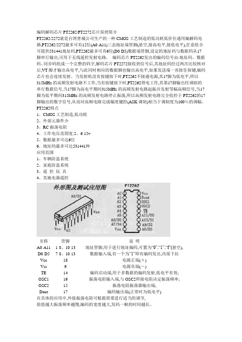
PT2262特点1、CMOS工艺制造,低功耗2、外部元器件少3、RC振荡电阻4、工作电压范围宽:2、6-15v5、数据最多可达6位6、地址码最多可达531441种应用范围1、车辆防盗系统2、家庭防盗系统3、遥控玩具4、其她电器遥控名称管脚说明A0-A11 1-8、10-13 地址管脚,用于进行地址编码,可置为“0”,“1”,“f”(悬空),D0-D5 7-8、10-13 数据输入端,有一个为“1”即有编码发出,内部下拉Vcc 18 电源正端(+)Vss 9 电源负端(-)TE 14 编码启动端,用于多数据的编码发射,低电平有效;OSC1 16 振荡电阻输入端,与OSC2所接电阻决定振荡频率;OSC2 15 振荡电阻振荡器输出端;Dout 17 编码输出端(正常时为低电平)在具体的应用中,外接振荡电阻可根据需要进行适当的调节,阻值越大振荡频率越慢,编码的宽度越大,发码一帧的时间越长。
变频器驱动光耦PC923引脚功能及控制原理
变频器驱动光耦PC923引脚功能及控制原理在变频器中我们会经常看到一种型号为PC923的元件,这个PC923元件是集成电路的一种,那么对于PC923的引脚功能朋友们熟悉吗?它的控制原理和控制特点朋友们掌握了吗?下面由广州科誉变频器维修培训中心的司工给朋友们详细的介绍一下变频器驱动光耦PC923引脚功能及控制原理,希望大家能喜欢。
对于PC923元件,由于它内部的控制是利用光电发射二极管和光电接收二极管进行控制的,生产厂家给它取了一个好听的名字叫光电耦合器,又由于它在变频器中是用在驱动电路中,变频器维修行业的专家们俗称它为驱动光耦。
PC923的实物图及引脚结构图请参看图一图二。
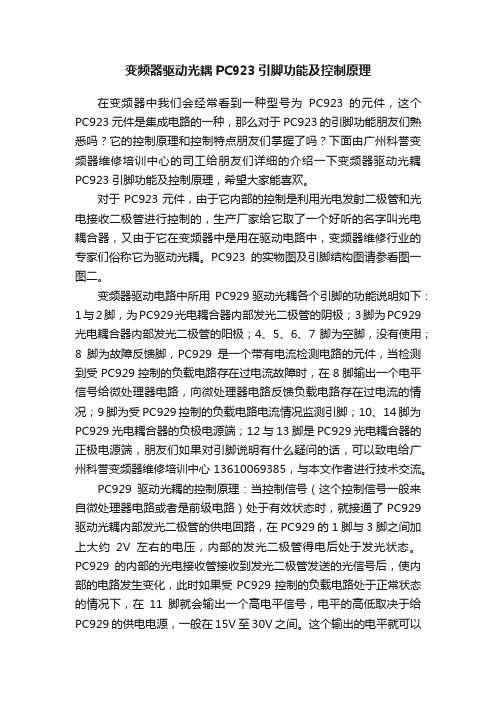
变频器驱动电路中所用PC929驱动光耦各个引脚的功能说明如下:1与2脚,为PC929光电耦合器内部发光二极管的阴极;3脚为PC929光电耦合器内部发光二极管的阳极;4、5、6、7脚为空脚,没有使用;8脚为故障反馈脚,PC929是一个带有电流检测电路的元件,当检测到受PC929控制的负载电路存在过电流故障时,在8脚输出一个电平信号给微处理器电路,向微处理器电路反馈负载电路存在过电流的情况;9脚为受PC929控制的负载电路电流情况监测引脚;10、14脚为PC929光电耦合器的负极电源端;12与13脚是PC929光电耦合器的正极电源端,朋友们如果对引脚说明有什么疑问的话,可以致电给广州科誉变频器维修培训中心136****9385,与本文作者进行技术交流。
PC929驱动光耦的控制原理:当控制信号(这个控制信号一般来自微处理器电路或者是前级电路)处于有效状态时,就接通了 PC929驱动光耦内部发光二极管的供电回路,在PC929的1脚与3脚之间加上大约2V左右的电压,内部的发光二极管得电后处于发光状态。
PC929的内部的光电接收管接收到发光二极管发送的光信号后,使内部的电路发生变化,此时如果受PC929控制的负载电路处于正常状态的情况下,在11脚就会输出一个高电平信号,电平的高低取决于给PC929的供电电源,一般在15V至30V之间。
各厂家中九接收机芯片IC资料大全(目前最完整的)部分附针脚定义

各厂家中九接收机芯片IC资料大全(目前最完整的)部分附针脚定义最新刷机资料点下面的链接最新刷机资料1最新刷机资料24月3日BIN教程工具集中帖刷机教程大全刷机工具大全2.10-3.2刷机bin大全3月3日后刷机bin大全各厂家中九接收机顶盒芯片IC资料大全(目前最完整的),部分附针脚定义。
方便大家速查。
可使用CTRL+F,然后输入相关数据进行速查,或者也可以下载附件。
品牌产品型号芯片配置海尔2晶10芯IC:HI2023E+1108+5812海尔高清OST-666 2晶6芯IC:M88VS2000+241674K.1+M88TS2020海尔高清OST-666 3晶12芯IC:High032E+His121+M88TS2020海尔3晶10芯(9针接口)IC:HI2023E+1108+5812+ESMTM12L64164A-GNR1T80AB 海尔高清OST-666 2晶6芯IC:Hi2023E+3160+TS2020欧视达ABS-209B 3晶10芯IC:GX3001+GX1121+LW37 欧视达ABS-209B 3晶11芯IC:GX3001+5037+8211欧视达ABS-309B 3晶11芯IC:GX3001+GX1121+MGCE5037欧视达AS-900S 1晶11芯IC:GX6121+25L80+LW37城市之宝BEX868 Y32S-93AT 2晶10芯IC:HTV903F+A VL1108+TS2020通达Y35S-8BAT/Y35S-8CAT 2晶10芯IC:HTV903+A VL1108+5812通达Y30S-01BT 2晶12芯IC:HTV903+A VL1108+2020 皇朝HSR-268 10芯IC:Hi2023+A VL1108+5812小霸王TDX-668E ABS-S1 1晶6芯IC:Hi2023+Hi3102+FT8211+HT1117天地星小霸王TDX-328B 1晶10芯IC:ALi M3328F+5810天地星小霸王TDX-668A (9针接口)IC:HI2023+1108+夏普头天地星小霸王TDX-668B 2晶振IC:HTV903+A VL1108EGA+RDA5812+25L8005天地星小霸王(三星数码王)TDX-668B 单晶6芯.针脚定义①-TXD ②-RXD ③VCC ④-GND ⑤-BL IC:Hi2023E+RDA5812+A VL1108E+MXT8211a+25L8005天地星(原大盒中星九号)3晶IC:Hi2023+1108+5037天地星TDX-668B 2晶10芯IC:Hi2023+A VL1108+5812天地星小霸王TDX-668C 2晶6芯IC:HTV903+A VL1108EGA+RDK5812+25F80小霸王TDX-328B 1晶10芯IC:ALi M3328F+5810小霸王TDX-668B 6芯IC:Hi2023+RDA5812+A VL1108E 小霸王TDX-668B 2晶6芯IC:HTV903+1108+5812小霸王TDX-668E 1晶6芯IC:Hi2023EC+Hi3121+5812 小霸王TDX-668E 2晶6芯IC:HTV903+1108+5812小霰王XC-B298 1晶12芯IC:HTV903-RDA5812-A VL1108 小霸王ABS-1388 2晶10芯针脚定义①-GND ②-RXD ③-TXD ④VCC小霸王ABS-1688 2晶10芯针脚定义①-GND ②-RXD ③-TXD ④VCC IC:Hi2023EC+Hi3122E+5812小霸王GF902 IC:A VL1118a+A V2020+EN25F80索尼高清ABS-S 258 2晶10芯针脚定义①-GND ②-RXD ③-TXD ④VCC IC:Hi2023EC+Hi3122E+5812索尼高清ABS-S 258 2晶10芯针脚定义①-GND ②-RXD ③-TXD ④VCC IC:Hi3102E+Hi2023EC+A V2020太阳红TYH-279ABS/289ABS/299ABS 2晶10芯针脚定义①-GND ②-RXD ③-TXD ④VCC松下科技星TDX-668B1/松下科技星-668EIC:Hi3102E+Hi2023EC+5812松下科技星TDX-668B 2晶6芯IC:HTV903FH42+A VL1108EGA+RGK5812松下科技星668B 2晶6芯Hi2023(E0908)+EVl1108EG2+5812松下科技星-668C 2晶6芯针脚定义①-RX .②-TX .③-GND .④VCC. ⑤-BLIC:A VL1108EG+HTV903F+5812松下科技星668E 2晶6芯IC:HV903+A VL1108E+5812松下科技星/海尔数码/海信数码单双晶6芯IC:Hi2023E+Hi3102(Hi3121)+5812松下科技星TDX-668B 2晶6芯针脚定义①-RXD .②-TXD .③-GND .④VCC. ⑤-BLIC:Hi2023+A VL1108+5812+25L8005松下高清SX168 3晶6芯IC:HTV903F+A VL1108+A V2020 松下数码王P-269A 2晶6芯IC:Hi2023E+Hi3122+A V2020 松下高清OST168 2晶10芯IC:Hi2023E+Hi3121+A V2020 松下科技PS-228 11芯IC:Hi2023+Hi3122+5812松下科技PS-228 2晶6芯IC:M88VS2000+M88TS2020+ES261474K松下科技PS-228 1晶12芯N88VS2000+ES261344K+M88TS2020高频头+T25P80+S163816STS松下科技PS-228 2晶IC:HTV903+1108+2020松下科技PS-228 2晶10芯IC:GX3001+GX1211+5812松下数码王OST-266 10芯(4针)针脚定义①-GND ②-RXD ③-TXD ④VCCIC:Hi2023E+Hi3106+2020松下数码王OST-266 2晶6芯IC:M88VS2000+M88TS2020+261414k+25F80松下数码王OST-266 2晶6芯IC:Hi2023E+Hi3102E+M88TS2020+MXT8211松下高清OST-466 2晶10芯IC:Hi2023e+Hi3121+MBBTS2020+MBDA80CG松下科技星3晶6芯IC:Hi2023+A VL1108+WGCE5037松下科技星.海尔数码.海信数码单双晶+6芯IC:Hi2023E+Hi3102(3121)+5812中星科技单晶14芯IC:Hi2023E+1108+5812+25L8单晶14芯中星科技ZG-N02 12芯IC:GX3001+A V2020中星科技2晶10芯针脚定义①-GND ②-RXD ③-TXD ④VCCIC:Hi2023EC+Hi3102E+5812+M12L64164A中兴科技ABS-S323 2晶10芯IC:Hi2023EC+HI3102E+5812+M12L64164A村村通ABS-S323- 2晶10芯针脚定义①-GND ②-RXD ③-TXD ④VCCIC:Hi2023EC+Hi3122E+5812村村通2晶6芯IC:HN4+0001+5812村村通ZL5188 1晶13芯IC:HTV903+1108+SHARP高频头村村通ZL-5188A 2晶11芯IC:HTV903+A VL1108+RDK5812村村通ZL-5188B 2晶13芯IC:HTV903+A VL1108+RDK5812 村村通ZL-5188B 2晶10芯IC:HTV903+A VL1108EGA+5812村村通ZL5188B 1晶13芯IC:HTV903+A V1108+SHARP6306村村通ZJ-11 IC:HTV903+1108+夏普头S7ZH6306村村通wx-666 3晶10芯IC:GX3001+GX1121+RDK5812村村通ZL-6188 2晶10芯IC:HTV903+A VL1108EGA+5812村村通ZL-6188C 10芯IC:GX3001+GX1121+RDK5812村村通DTH(铁壳) 3晶12芯IC:A VL1108EG+HTV903F+A V2020村村通001 3晶10芯IC:GX3001+GX1121+RDK5812村村通ABS-S GD-1008 3晶10芯IC:Hi2023E+A VL1108E+ZL10037+F16-100HIP村村通ABS-S888AIC:Hi2023EC+Hi3121+ET8211+RDA5812+25X80视美人ABS-S PS-1288 2晶10芯IC:Hi3102E+Hi2023EC+A V2020视美人PS-1288 ICM88VS2000+ES256454K+M88TS2020 视美人2晶10芯IC:Hi2023+3106+A V2020太平鸟HJ321 3晶10芯针脚定义①-GND .②-RXD .③-TXD .④VCCIC:GX3001+GX1121+TS2020太平鸟HJ321 3晶11芯IC:GX3001+GX1121+5812焦点yj5888 2晶10芯IC:HTV903+A VL1108+RDA5812幸运之星YJ5988 2晶10芯IC:HTV903F+A VL1108EGa+A V2020克莱尔HT701 1晶10芯IC:A VL1108EG+HTV903F+M88TS2000中电电子J-6288 ABS-S 3晶12芯IC:GX3001+GX1121+5812小福星3晶11芯针脚定义①-GND .②-(空) .③-RXD .④-TXD ()IC:GX3001+GX1121+5812东仕DIS-2000K 单晶10芯IC:HTV903F+A VL1108E+A V2020Souy Ericsson英文机2晶10芯IC:GX3001+GX1121+A V2020高斯贝尔/歌德威尔ABS-208F 3晶14芯针脚定义①-GND .②-TXD .③-RXD .④VCC .⑤-BL IC:A VL1108EG+Hi2023+5812高斯贝尔ABS-208 1晶14芯(5针).针脚定义①-GND .②-TXD .③-RXD .④VCC .⑤-BL IC:A VL1108EG+Hi2023+5812歌德威尔ABS-208H/高斯贝尔208P 3晶14芯针脚定义①-GND .②-TXD .③-RXD .④VCCIC:M3330E+A VL1108EG+A V2020+M12L64164高斯贝尔ABS-208P/歌德威尔208H 1晶14芯针脚定义①-GND .②-TXD .③-RXD .④VCC .⑤-BL IC:A VL1108EGi+Hi2023+5812高斯贝尔ABS-208P/歌德威尔208H 1晶14芯针脚定义①-GND .②-TXD .③-RXD .④VCCIC:M3330E+A VL1108EG+A V2020+M12L64164A高斯贝尔ABS—208F IC:Hi2023+A VL1108EGA+M88TS2020高斯贝尔ABS—208 2晶14芯IC:HTV903+1108+5812吉祥ABS-208C IC:Hi2023+A VL1108EGa+GST GAIM-18R ABS-STUNER吉祥ABS-2009B 3晶14芯IC:GX3001+GX1121+RDK5812吉祥ABS-2009大铁壳2晶IC:GX3001+GX1121+夏普高频头ABS-2009 2晶12芯IC:HTV903+1108+GAIM-18R歌德威尔ABS-208 3晶6芯IC:D61216GJ+1108+5812歌德威尔ABS-208 3晶14芯(9针接口)IC:M3330+1108+5812高斯贝尔ABS-208 3晶(9针母串口)IC:A VL1108+Hi2023+GAIM-18RIC:D61216GJ100+A VL1108EG+S29AL016D70TF102+ISSI高斯贝尔ABS-208N 铁壳(9针母串口) IC42s16400F高斯贝尔ABS-208 IC:D61216GJ+A V1108+29AL016D+5812高斯贝尔ABS-208S 1晶IC:NECD61216GJ+A VL1108EGa+高频头高斯贝尔ABS-208Q 1晶14芯IC:A VL1108EGA+M3330E+M12L64164A+A V2020ABS-S LX-3688A 1晶12芯IC:GX3001+GX1121+5812现代V4、V5 3晶9芯IC:GX3001+GX1121+5812+EN25D80+HY57V641620ETP-6 集信科技V6铁壳(海尔机芯) 3晶9芯针脚定义①VCC .②-TXD .③-RXD .④-GNDIC:1108EG(Hi3121)+Hi2023+5812.集信科技V4.V6(铁壳) 2晶9芯( B型)针脚定义①VCC .②-RXD .③-TXD .④-GNDIC:0001(GX3001)+HN4F74+5812集信科技V4 .V6(铁壳) 2晶10芯针脚定义①VCC. ②-RXD .③-TXD .④-GNDIC:00001(GX3001)+HN4LSW+S6416AHTA+5812集信科技V4.V6(铁壳)IC:HN4LSW+S6416AHTA-6BZH+EN25F80-1000CP+5812集信科技V4.V6(铁壳)IC:0002P1M43700ta06+5812+EN25F80+TM8211+POL4558 集信科技V4.V5 1晶10芯(A型)针脚定义①VCC .②-RXD .③-TXD .④-GNDIC:0002(GX6121)+5812+M12L64164A艾雷特2晶10芯IC:M88VS2000+ES256454K+M88TS2020艾雷特V5IC:HN4F910931M2EE+0001G1K729-1TA060932+5812艾雷特ALT5812 IC:GX3001+GX1121+5812艾雷特ALT600A 2晶11芯IC:M3330E+A VL108的+夏普高频头艾雷特ALT600A/吉祥ABS-2009 2晶IC:GX3001+GX1121-ES29L160FB+SHARP高频头艾雷特ALT600GIC:HTV903+A VL1108+25L160+ST2020(Y32S-8BAT 081113)艾雷特ALT6812 1晶10芯IC:GX6121+RDA5812+ZB-1A艾雷特ALT6815 1晶10芯IC:GX6121-RDA5812-2B-1A艾雷特ALT7815 3晶10芯IC:GX3001+1121+TS2020艾雷特1000 黑珍珠V4.V5 1晶10芯IC:0002(GX6121)+EEPLDA+5812+M12L64164A艾雷特alt 7812 3晶10芯IC:GX3001+GX1121+5812艾雷特ALT7812 3晶11芯针脚定义①VCC .②-RXD .③-TXD .④-GNDIC:GX3001+GX1121+5812艾雷特ALT600c 2晶10芯IC:GX3001+GX1121+5812艾雷特ALT600c 2晶11芯IC:GX3001+GX1121+5812艾雷特ALT600c 1晶11芯IC:CH216H+A VL1108+C6XS-8CA深圳亿通DVB-V5 10芯IC:HN4N46+EN25F80+G1N540-1TA06+IS42S16400-7T+581亿通电子WS-3688ZL 1晶10芯IC:Hi2023EC+Hi3102E+A V2020中大WS-3688ZJ (铁壳) 1晶10芯针脚定义①-GND .②-RXD .③-TXD .④VCCIC:Hi2023EC+Hi3102E+A V2020中大WS-3688ZJ (铁壳) 2晶10芯IC:Hi2023+A VL1108EG+夏普高频头皇视HSR-208A 2晶10芯IC:Hi2023E+A VL1108EG+A V2020皇视HSR-208B 2晶10芯IC:Hi2023+1108+2020皇视HSR-208B 单晶10芯IC:3330+1108+2020皇视HSR-208B 单晶10芯针脚定义①-GND ②-TXD ③-RXD ④-VCCIC:Hi2023EC+Hi3102+A V2020皇视HSR-2090 2晶11芯IC:Hi2023+1108EGa+夏普头++EN29LV160皇视HSR-210A 单晶6芯IC:Hi2023ec+Hi3122e+A V2020 皇视HSR-260A 铁盒2晶10芯IC:Hi+1108+SHARP夏普头皇视HRS-268 3晶10芯IC:Hi2023EC+Hi3102E+A V2020 皇视HRS-268 2晶10芯IC:Hi2023EC+Hi3121+5812皇视HSR-268 单晶10线IC:HTV903+A VL1108+5812皇视HSR-268 单晶10线IC:Hi2023+Hi3121+A V2020皇视HRS-268 3晶10芯IC:Hi2023EC+A VL1108+5812皇视HSR-260B 3晶10芯IC:Hi2023+1108+2020皇视HSR-260B/索尼高清258 1晶10芯IC:2023E+3121+A V2020皇视HSR-260B 3晶10芯IC:HI2023+1108+5812皇朝HSR-268 10芯IC:Hi2023+A VL1108+5812凯恩斯KES-2066S 6芯针脚定义①-TXD .②-RXD .③VCC .④-GND .⑤-BL IC:Hi3122E+Hi2023ECE+N25F80凯恩斯KES-2077Z 1晶6芯针脚定义①-TXD .②-RXD .③VCC .④-GND .⑤-BL IC:Hi2023EC+3122E+5812凯恩斯2077ABS 2晶10芯IC:M3330+A VL1108+5812凯恩斯2077ABS 2晶10芯IC:Hi2023+1108E+5812+25L800凯恩斯KES-2088S 2晶6芯IC:Hi2023EC+HI3102E+RDA5812凯恩斯KES-2088S 2晶10芯IC:Hi2023EC+HI3102E+RDA5812凯恩斯KES-2088S 2晶6芯针脚定义①-TXD .②-RXD .③VCC .④-GND .⑤-BL IC:Hi2023EC+HI3122E+RDA5812凯恩斯KES-2088Z (5针).针脚定义①-TXD .②-RXD .③VCC .④-GND .⑤-BL IC:Hi2023EC+HI3102E+RDA5812凯恩斯KES-2099S 2晶6芯IC:Hi2023EC+Hi3102E+5812+25L80凯恩斯KES-2188T 3晶10芯IC:Hi2023+1108+5812凯恩斯KES-2188T 3晶12芯IC:Hi2023+1108E+5037凯恩斯KES-2288S 3晶10芯IC:M3330E+A VL1108+RDA5812+M12L64164A凯恩斯KES-2688b 2晶10芯IC:Hi2023e+1108e+5812 凯恩斯KES-2688S 2晶10芯IC:Hi2023e+1108e+5812凯恩斯KES-2788S 3晶10芯IC:Hi2023E+A VL1108EGa+5812凯恩斯KES-2788S 2晶6芯IC:Hi2023EC+Hi3122E+5812凯恩斯KES-5188 11芯IC:HTV903+A VL1108EGA+A V2020凯恩斯KES-5188A铁盒2晶10芯IC:HTV903F+A VL1108+RDK5812+F80+PT8211凯恩斯KES-5188B 2晶13芯IC:HTV903+RDA5812+A VL1108+8211+F80美路3晶13芯IC:Hi2023E+1108+2119美路2晶12芯IC:GX3003+GX1121+5812美路MR-1809 IC:Hi2023E+A VL1108E+高频头MAX2119C 美路MR-5598铁壳3晶12芯IC:GX3003+GX1121+5812 美路MR-5598 3晶12芯针脚定义①VCC. ②-RXD .③-TXD .④-GNDIC:Hi2023E+1108+2119C美路-5798 IC:Hi2023E+1108+2119C美路-5598 IC:Hi2023+1108+GAIM-18R+29lv160ZY 5518A 2晶10芯IC:Hi2023E+3102E+5812万利达ZY-5518A 1晶6芯((5针))IC:Hi2023E+Hi3102E+5812万利达ZY-5518A 2晶10芯IC:CX3001+GX1121+5812万利达ZY-5518A 3晶10芯(9针接口)IC:Hi2023+1108+5812长虹新一代3晶10芯IC:HI2023E+1108E+FL016ALF长虹新一代,海尔数码、海信数码单双晶体6芯IC:HI2023E+3102(3121)+5812长虹数码CH930 3晶12芯IC:HTV903F+1108+A V2020+M80长虹精品TC-6688ABS 2晶10芯IC:HTV903+A VL1108EG+5812长虹精工YJ5978 1晶10芯IC:HTV903F+1108EGa+2000+F80-100+8211长虹KES-2099S 2晶5芯IC:Hi2023+Hi3102E+5812长虹KES 2晶6芯IC:Hi2023+Hi3102+5812长虹CH920 3晶6芯IC:HTV903F+1108EGa+A V2020+25L80航天天信WTD198J 2晶12芯(9针接口)IC:GX3001+GX1121+5812+ES29LV160FB-70TG航天珠江WTD-198J 2晶12芯IC:GX3001+GX1121+5812 航天珠江ABS-209B IC:GX3001+GX1121++WGSE5037航天数码ABS-3809 2晶12芯IC:GX3001+GX1121+5812航天直播HT-168 3晶12芯IC:Hi2023+1108+夏普头航天高清王-HS-166 2晶12芯IC:Hi2023EC+Hi3102E+RDA5812航天高清王HS-169 2晶12芯针脚定义①-GND .②-TX .③-RX .④-VCCIC:Hi2023EC+3122+5812天诚TCD-219ABS 2晶10芯IC:M3330E+A VL1108EGA+5812天诚TCD-299Z 2晶10芯IC:Hi2023+3206+5812天诚TD-299Z 2晶5芯IC:Hi2023+3206+5812天诚TD-2992 2晶6芯IC:Hi3122E+Hi2023E+5812+F80+MXT8211天诚539 2晶10芯IC:HTV903+A V1108+5812天诚519型2晶10芯IC:HTV903+1108E+5812天诚TCD-239ABS 3晶10芯IC:M3330+1108+5812 天诚TCD-239ABS 2晶10芯IC:Hi2023+1108E+5812 天诚TCD-239 2晶10芯IC:M3330E+1108E+5812天诚TCD-299ABS 2晶10芯IC:Hi2023EC+Hi3121+5812天诚TCD-319ABS 3晶10芯IC:Hi2023E0914+A VL1108EGa+RDA5812天诚TCD-319ABS 3晶12芯IC:Hi2302+A VL1108+5037 天诚TCD-369ABS 3晶10芯IC:Hi2023+1108+5812天诚TCD-369ABS 3晶10芯IC:M3330E+1108+5812天诚TCD-369ABS 3晶5芯IC:Hi2023+1108+WCGE5037天诚TCD-509ABS 3晶10芯IC:M3330E-A VL1108EGa-5812天诚TCD-509ABS 10芯(5针)IC:Hi2023+A VL1108+5812+M12L6416A天诚TCD-539ABS 2晶10芯(5针)针脚定义①-RX .②-TX .③VCC .④-GND .⑤-BLIC:M3330E+A VL1108+25L80+5812天诚TCD-579ABS 2晶10芯IC:Hi2023+Hi1108+5812天诚TCD-579ABS 3晶10芯IC:HiM3330+A VL1108EGa+RDA5812天诚TCD-589ABS 3晶10芯IC:Hi2023+1108+5812天诚TCD-689ABS铁壳机2晶12芯(9针接口)IC:Hi2023+A VL1108+夏普头天诚TC-ABS1108A 11芯IC:Hi2023EC+A VL1108+5812 TCD--239ABS 2晶10芯IC:M3330E+A VL1108E+5812 TCD-339ABS 3晶10芯(9针接口) IC:Hi2023+1108+5812TCD-509ABS 3晶10芯IC:Hi2023E0915+A VL1108EGa+RDA5812TCD-509ABS 2晶10芯(5针) IC:Hi2023EC+HI3121+5812TCD-519ABS 2晶10芯IC:Hi2023+A VL1108+5812TCD-599 2晶10芯IC:M3330+A VL1008+5812TCD-219ABS 2晶振10芯针脚定义①-TXD .②-RXD .③-VCC .④-GND .⑤-BLIC:Hi2023EC+Hi3121+5812爱普思DVB-2568 3晶10芯IC:HTV903+1121+2020卓异5518A 3晶10芯IC:Hi2023E+1108+5812卓异5518A(铁壳)3晶11芯IC:Hi2023E+1108+5812卓异5518A(铁壳)2晶11芯(9针接口) IC:Hi2023+1108+夏普独立高频头卓异5518A G 1晶10芯爱百信针脚定义①-GND .②-TXD .③-RXD .④VCCIC:HTV903+A VL1108+5812卓异ZY-5518A G 驰骋天下针脚定义①-GND .②-RXD .③-TXD .④VCCIC:HTV903+A VL1108+5812+F80卓异5518AG 2晶11芯针脚定义①-GND .②-RXD .③-TXD .④VCC ⑤-BL IC:Hi2023E+1108+5812卓异ZY-5518A H 春1晶6芯针脚定义①-GND .②-TXD .③-RXD .④VCCIC:GX3001+5812+25L8005卓异ZY-5518A H 春2晶10芯针脚定义①-GND .②-TXD .③-RXD .④VCC .⑤-BLIC:Hi2023E+HI3121+5812+F25L008A卓异ZY-5518A H 秋针脚定义①-GND .②-RXD .③-TXD .④VCC 升级接口在内部PCB上IC:GX6121+5812+F80卓异ZY-5518A H 秋1晶10芯针脚定义①-GND .②-RXD .③-TXD .④VCC ⑤-BLIC:Hi2023EC+Hi3102E+5812+F80-100卓异ZY-5518A H至尊王牌2晶10芯针脚定义①-GND .②-TXD .③-RXD .④VCCIC:GX3001+GX1121+5812+25L8005卓异ZY-5518A H 财富2晶6 芯针脚定义①-GND .②-TXD .③-RXD .④VCC .⑤-BLIC:芯片掩磨+5812+80L100绿达PS-1288 3晶12芯IC:Hi2023E+ABS090520+M88TS2020绿达PS-1288 2晶12芯IC:Hi2023+Hi3021+A V2020绿达视美人\卓异1晶10芯IC:Hi2023EC+Hi3121+2020 绿达金统帅3晶10芯IC:M3330+1108+5812三星DQ88/DQ66 IC:HTV903F+A VL1108+A V2020三星高清王2晶12芯IC:GX3001+GX1121+5812三星高清DQ88 3晶12芯IC:HTV903F+A VL1108+A V2020 三星数码王TDX668B 2晶6芯针脚定义①-RXD .②-TXD .③-GND .④VCC. ⑤-BLIC:Hi2023+1108+5812三星数码王TDX668B 2晶6芯IC:HTV903F+A VL1108E+5812三星数码王668C 2晶6芯IC:HTV903F+A VL1108E+5812三星数码王TDX668E 1晶6芯IC:Hi2023EC+3102C+5812三星HSR-208C 1晶10芯IC:Hi2023E+Hi3102+MXT8211+A V2020+F25L08pA三星小霸王ABS-S 2009 2晶10芯IC:CX3001+CX1121+5812三星小霸王2900 (9针接口)IC:Hi2023E+A VL1108+MAX2119三星王国-KL6350 1晶11芯IC:HTV903+A VL1108EGa+EDA5812开门红KSP638 2晶10芯IC:HTV903F+A VL1108E+A V2020开门红KSP638 1晶10芯IC:CT216H+A VL1108EGa+A V2020日立创新TDX-668B 2晶6芯针脚定义①-RXD .②-TXD .③-GND .④VCC. ⑤-BLIC:Hi2023+A VL1108+5812志高之星HS166 2晶12芯IC:Hi3102+Hi2023+5812志高之星HS169 2晶12芯IC:Hi2023EC+Hi3012E+RDA5812A+EM638165TS-6G金牛ABS-1108 3晶10芯IC:Hi2023+1108+5812小灵通2晶6线IC:Hi2023+1108+5812福临门ABS-S 3晶9线IC:GX1121+GX3001+5812C60S-93AT 单晶10芯IC:CT216H+A VL1108EGa+A V2020 ABS-2301 单晶10芯针脚定义①-GND.②-TXD.③-RX .④VCCIC:Hi2023EC+Hi3211E+5812+25L8005其乐达CT216 2晶10芯IC:CT216+1108+A V2020科海6228 1晶11芯IC:HTV903+A VL1108EGa+RDa5812+25X16A VSIG科海6228-CT216H 1晶11芯IC:CT216H+1108EGa+M88TS2020科海C623S-91AT 单晶10芯IC:CT210H+A VL1108+2020 科海炫彩6888 IC:HTV903+A VL1108EGa+RDa5812科海2888(小天使)2晶10芯IC:HTV903+A VL1108EGa+RDa5812大旗920 3晶12芯IC:HTV903+A VL1108+A V2020大旗DQ920 3晶12芯IC:GX3001+GX1121+5812+25X16 大旗930 3晶12芯IC:HTV903+A VL1108+A V2020众昌电子ABS--2088 2晶10芯IC:Hi2023+A VL1108+5812众昌电子ABS-2087 2晶10芯IC:M3330+A VL1108+5812 创维S600 3晶IC:M3330E+A VL1108E+5812创维新一代3晶10芯IC:Hi2023E+1108+5037+FL016A 中广通XC-B188 3晶12芯IC:GX3001+GX1121+5812深圳知音ABSTAR KT-2309 3晶10芯IC:Hi2023+A VL1108E+5812知音科技ABSTAR KT1028H 2晶振10芯IC:Hi2023+A VL1108+GST GAIM-18R铁壳ABS-2009 2晶11芯IC:Hi2023+1108+夏普头王牌数码OST-366 2晶6芯针脚定义①-GND ②-RXD .③-TXD .④VCCIC:Hi3102+Hi2023EC+A V2020王牌数码王GM-ABS1108A 2晶10芯针脚定义①-GND .②-TXD .③-RXD .④VCCIC:GX3001+GX1121+5812+25L8005王牌数码王GM-ABS1108A 10芯IC:Hi2023+A VL1108+5812JIXIANG ABS-208 2晶14芯(9针接口)IC:Hi2023+1108+GST GAIM-18R ABS TUNER 夏普头JIXIANG-ABS208 2晶IC:D6121+1108+GST高频头East Star 2晶10芯IC:M3330-1108-GST GAIM-18R高频头小福星abs 2008 3晶12芯IC:GX3001+GX1211+5812通达C60S-93AT/C62S-91AT 1晶10芯IC:CT216H+A VL1108E+2020威特斯ZL-5188A 2晶13芯IC:HTV903+A VL1108+RDK5812威特斯ZL-5188B 2晶11芯IC:GX3001+GX1121+5812迷你星3晶13芯IC:GX3001+GX1121+5812+F16-100HIP高星HS-312 3晶12芯IC:GX3001+GX1121+5812北大高科3晶9芯IC:GX3001+GX1211+5812思达科ABS-S 801型2晶10芯IC:GX3001+GX1121+5810思达科ABS-S 802G 2晶10芯IC:GX3001+GX1211+5812思达科ABS-S 803A 1晶10芯IC:A VL1118+A V2020+25D80V思达科ABS-S 803G IC:GX3001+GX1211+5812思达科ABS-S 806H IC:GX3001+GX1211+5812思达科ABS-S 806H IC:A VL1118+A V2020+DSD4M16G思达科ABS-S 806H IC:HN4J7G+G2A954+5812+25X80思达科ABS-S807 1晶5芯IC:A VL1118a+A V2020+806H金霸王JBW-6688 2晶11芯IC:HTV903F+A VL1108EGa+A V2020+8211金霸王JBW-6688 IC:GX3001+GX1211+5812阿德尔ADE-168 IC:HY903+A VL1108EG+A V2020阿德尔ADE131金刚IC:HTV903F+A VL1108E+M88TS2020 海西小霸王TD299Z 2晶6芯IC:Hi2023E+Hi3122+5812 同洲CY-668S 1晶12芯IC:HM1512+1108+5812喜旺ABS5398 IC:Hi2023+1108E+MAX2119C喜旺ABS-5798 12芯IC:GX3001+GX1211+5812喜旺ABS-3809 2晶12芯IC:GX3001+GX1121+RDA5812希旺598 2晶12芯(9针接口) IC:Hi2023+1108+SHRP 高频头彩虹视霸CY84 1晶10芯IC:HTV903F+A VL1108+M88TS2020彩虹视霸A10S-9AAT 1晶10芯IC:A VL1118+SM42S16400B1-7+F80九洲村村通DVS-398F IC:CT216H+ALV1108+SHRP高频头金星ABS-208 1晶14芯IC:Hi2023+A VL1108+铁壳高频头威克2晶6芯(5针) IC:HTV903+1108+5812华尔HR731A1 3晶12芯IC:CX3001+CX1121+SHARP高频头爱普斯3晶9芯IC:HTV903+A V2020+A VL1108EG爱普斯2568 3晶10芯IC:HTV903+A V2020+A VL1108EG 爱普斯IC:GX3001+GX1211+A V2020+2J10X未来视佳ADEI88 3晶9芯IC:HTV903F+A V2020+A VL1108EG黑金刚TRT006 1晶10芯IC:A VL1118+A V2020+4558+F80-100DX-668 2晶10芯针脚定义①-RXD .②-TXD .③VCC .④-GND .⑤-BLIC:Hi2023EC_Hi3102E+5812+F80-100傲天海-吉祥2晶12芯针脚定义①-GND ②-RXD ③-TXD ④VCCIC:GX3001+GX1121+RDA5812高频头+P8075火星漫步LJ6008 1晶10芯IC:HTV903F+A VL1108+M88TS2020+F80-100王牌新一代TD-299Z针脚定义①- . ②-TXD .③-RXD .④-GND ⑤-IC:Hi2023E+Hi3122+5812王牌HJ360 3晶10芯IC:GX1120+GX3001+TS2020TVWALKER ABS-2008 1晶6芯IC:D61216GJ+1108E+SHARP头吉祥988 (ZJ-111) 1晶11芯IC:HTV903 +1108+高频头北京北电科林3晶12芯IC:Hi2023+A VL1108EGa+SHARP高频头家家福BEX811 1晶10芯IC:24645K2+M88VS2000+M88TS2020家家福ADE158 IC:HTV903+A VL1108+M88TS2020华星科技2晶IC:Hi2023+A VL1108+5812亚视达ABR-S(H11) 2晶10芯IC:HTV903+1108E+A V2020HSTAR 3晶10芯IC:Hi2023+A VL1108EGa+M88IS2020长江电讯ABS-2008型铁壳(9针接口)IC:D61216GJ+A VL1108EG+夏普头全家福3晶IC:Hi2023E+A VL1108EG+M88TS2020 畅想BEX818 1晶10芯IC:HTV903+A VL1108+A V2020 必佳GF-901 2晶10芯针脚定义①-GND .②-RXD .③-TXD .④VCCIC:HTV903+1108+A V2020KSP600G 飓风(华亚) 2晶10芯针脚定义①-GND ②-TXD ③-RXD ④VCCIC:HTV903+1108+M88TS2020+25D80万家乐TB002 (5针)IC:Hi2023EC+Hi3102E+M88TS2020+25X80A V万家乐2晶6芯IC:M3330+ALi1108+5812+F80-75奥伟科技ABS-800 3晶(9针接口)IC:GX3001+GX1121+5812奥伟科技ABS-900E 2晶12芯IC:CT216+A VL1108+独立高频头GAIR-08R天眼HSTER3晶10芯IC:Hi2023E+A VL1108+5812飞翔ADE351 2晶10芯IC:HTV903F+A VL1108EG+M88TS2000星视通XC-B268 1晶10芯IC:HTV903+A VL1108+5812星视通XC-C268 1晶11芯IC:HTV903 A VL1108 5812奥维科技ABS-600 3晶12芯IC:GX3001+GX1121+A V2020 超的个人论坛转载分享本资源。
PC929_series
PC929 Series1.Recognized by UL1577 (Double protection isolation), file No. E64380 (as model No. PC929)2. Approved by VDE (VDE0884) (as an option) file No. 94626 (as model No. PC929)3. Package resin : UL flammability grade (94V-0)■ Features■ Agency approvals/Compliance1. Inverter■ ApplicationsHigh Speed, Built-in Short Protection Circuit, Gate Drive SMD 14 pin ∗OPIC Photocoulper1. 14 pin Half pitch type (Lead pitch : 1.27 mm)2. Double transfer mold package (Ideal for Flow Soldering)3. Built-in IGBT shortcircuit protector circuit4. Built-in direct drive circuit for IGBT drive(Peak output current : I O1P , I O2P : MAX. 0.4 A)5. High speed responce (t PLH , t PHL : MAX. 0.5 µs)6. High isolation voltage (V iso(rms) : 4.0 kV)■ DescriptionPC929 Series contains an IRED optically coupled to an OPIC chip.It is packaged in a Mini-flat, Half pitch type (14 pin).Input-output isolation voltage(rms) is 4.0kV. High speed responce (t PLH , t PHL : MAX. 0.5 µs).Notice The content of data sheet is subject to change without prior notice.In the absence of confirmation by device specification sheets, SHARP takes no responsibility for any defects that may occur in equipment using any SHARP ∗"OPIC"(Optical IC) is a trademark of the SHARP Corporation. An OPIC consists of a light-detecting element and a signal-processingcircuit integrated onto a single chip.■ Internal Connection Diagram■ Truth table■ Outline Dimensions(Unit : mm)Input ON OFFC input-output Low level Low level High level High levelO 2 output High level Low level Low level Low levelFS output High level Low level High level At operating protection functionHigh level1234567Cathode Cathode Anode NC ∗NC ∗NC ∗NC ∗891011121314FS C GND O 2GND∗No. to pin shall be shorted in the device.O 1V CC 47Product mass : approx. 0.47gDate code (2 digit)A.D. 1990 1991 1992 1993 1994 1995 1996 1997 1998 1999 2000 2001MarkABCDEFHJKLMNMarkPRSTUVWXABCMark123456789ONDMonthJanuaryFebruaryMarchAprilMayJuneJulyAugustSeptemberOctoberNovemberDecemberA.D20022003200420052006200720082009201020112012······2nd digitMonth of production 1st digitYear of productionrepeats in a 20 year cycle Country of originJapan■ Electro-optical CharacteristicsParameterSymbol MIN.TYP.MAX.UnitI n p u tForward voltage T a =25˚C, I F =0.2mA Reverse currentTerminal capacitance T a =25˚C, V =0, f =1kHz O u t p u tSupply voltageT a =−10 to +60˚C−O 1 Low level output voltage O 2 High level output voltage O 2 Low level output voltage O 1 leak currentHigh level supply current Low level supply currentT a =25˚C, V CC =V O1=24V, I F =0V CC =V O1=24V, I F =0V V µA pF V V V V µA mA mA mA mA T a =25˚C, I F =10mA T a =25˚C, V R =5V T a =25˚C, V CC =V O1=24V, I F =5mA V CC =V O1=24V, I F =5mA−−−1515−20−−−−−−1.2−1025030240.42.0500171918201.75Conditions V F1V F2I R C t V CC V O1L V O2H V O2L I O1L I CCH I CCLV CC1=12V, V CC2=−12V, I O1=0.1A, I F =5mA V CC =V O1=24V, I O2=−0.1A, I F =5mA V CC =24V, I O2=0.1A, I F =0T a =25˚C, V CC =V O1=35V, I F =0*8*9*9*9*9*9*9*9*9−30−−22V −0.21.2−10−11−1.61.5(unless otherwise specified T a =T opr )*8 It shall connect a by-pass capacitor of 0.01 µF or more between V CC (pin 13 ) and GND (pin, 10 , 14) near the device, when it measures the transfer characteristics and theoutput side characteristics.*9 FS=OPEN, V C =0■ Absolute Maximum RatingsParameter Symbol Rating Unit I n p u t Forward current mA Reverse voltage V O u t p u tSupply voltage V O 1 output current A A O 2 output current A A O 1 output voltage V Power dissipation Overcurrent detection voltage Overcurrent detection current Error signal output voltage Error signal output current mW V mAVmATotal power dissipation mWOperating temperature ˚C Storage temperature ˚CI F V R V CC I O1I O1P I O2I O2P V O1P O V C I C V FS I FS P tot V iso (rms)T opr T stg T sol ˚C *2*1O 1 peak output current *3*3*4O 2 peak output current *5*6Isolation voltage Soldering temperature *1 The derating factors of a absolute maximum ratings due to ambient temperature are shown in Fig.15*2 T a =25˚C *3 Pulse width ≤0.15µs, Duty ratio : 0.01*4.5 The derating factors of a absolute maximum ratings due to ambient temperatureare shown in Fig.16*6 AC for 1minute, 40 to 60 %RH, T a =25˚C, f =60Hz *7 For 10s206350.10.40.10.435500V CC30V CC 205504.0−25 to +80−55 to +125260kV*7(unless otherwise specified T a =T opr )ParameterSymbol MIN.TYP.MAX.UnitT r a n s f e r c h a r a c t e r i s t i c sP r o t e c t i o n o u t p u tE r r o r s i g n a l o u t p u tO v e r c u r r e n t d e t e c t i o nT a =25˚C,V CC =V O1=24V, FS =OPEN, V C =0V CC =V O1=24V, FS =OPEN, V C =0Isolation resistanceRise time Fall timeOvercurrent detection voltage Overcurrent detection voltage hysteresis widthO 2 "High →Low" propagation delay time at overcurrent protection O 2 "High →Low" output voltage at overcurrent protectionError signal output pulse widthO 2 Fall time at o vercurrent protection Low level error signal voltageHigh level error signal voltage Instantaneous common mode rejection voltage (High level output)Instantaneous common mode rejection voltage (Low level output)mA mA Ωµs µs µs µs kV/µskV/µs V V µs µs VVµAµs µs"Low →High " input threshold current T a =25˚C,V CC =V O1=24V, I F =5mA, R G =47Ω, C G =3 000pF FS =OPEN, V C =0T a =25˚C, V CM =600V(p-p) I F =5mA, V CC =V O1=24V, ∆V O2H =2.0V, FS =OPEN, V C =0T a =25˚C, V CM =600V(p-p) I F =0, V CC =V O1=24V,∆V O2L =2.0V, FS =OPEN, V C =0T a =25˚C V CC =V O1=24V I F =5mA, R G =47Ω C G =3 000pF, FS =OPEN T a =25˚C, I F =5mA V CC =V O1=24V I FS =10mA, R G =47Ω C G =3 000pF, C =OPEN T a =25˚CV CC =V O1=24V, I F =5mA V FS =24V, R G =47Ω C G =3 000pF, V C =0T a =25˚C, V CC =V O1=24V I F =5mA, R FS =1.8k ΩR G =47Ω, R C =1k Ω C G =3 000pF, C P =1 000pFT a =25˚C V CC =V O1=24V I F =5mA,R G =47Ω, C G =3 000pF, R C =1k Ω, C P =3 000pFFS =OPEN 5×10¹⁰−−−−−1.51.5V CC −6.512−−−−20−0.30.2−0.50.5−−V CC −5.5310−20.41005−3.05.00.50.5Conditions"Low →High" propagation delay time "High →Low" propagation delay time R e s p o n s e t i m eI FLH R ISOt PLH t PHL t r t f CM L V CTH V CHIS t PCOHL t PCOtf V OEV FSL I FSH t PCFHL ∆t FSCM HT a =25˚C, DC =500V, 40 to 60%RH−10110.20.21.50.30.3−−V CC −6245−0.2−135*11*12(unless otherwise specified T a =T opr )*10Error signal "High →Low"propagation delay time *10 It shall connect a by-pass capacitor of 0.01 µF or more between V CC (pin 13 ) and GND (pin 10 , 14) near the device, when it measures the device, when it measures theovercurrent characteristics, Protection output characteristics, and Error signal output characteristics.*11 I FLH represents forward current when output goes from "Low" to "High"*12 V CTH is the of C(pin 9 ) voltage when output becomes from "High" to "Low"■ Model Line-upPC929PC929Y−−−−−−Approved Lead Form Package Model No.VDE0884PC929P PC929PY−−−−−−Approved TapingSMT Gullwing1 000pcs/reel Sleeve 50pcs/sleeve Please contact a local SHARP sales representative to inquire about production status and Lead-Free options.Fig.6 Test Circuit for High Level / Low LevelSupply CurrentFig.5 Test Circuit for "Low →High" InputThreshold CurrentFig.1 Test Circuit for O 1 Low Level OutputVoltageFig.2 Test Circuit for O 2 High Level OutputVoltageFig.3 Test Circuit for O 2 Low Level OutputVoltageFig.4 Test Circuit for O 1 Leak CurrentFig.7 Test Circuit for Instantaneous CommonMode Rejection VoltageFig.8 Test Circuit for Response TimeFig.9 Test Circuit for Overcurrent Detection Voltage,Overcurrent Detection Voltage HysteresisFig.10 Test Circuit for O 2 Output Voltage atOvercurrent ProtectionGNDGNDV O2L V O2HV CM waveformV CM (peak)CM H , V O2 waveform SW at A, I F =5mA CM L , V O2 waveform SW at B, I F =0mAV10%90%V OUT 50%V INFig.12 Test Circuit for High Level ErrorSignal CurrentFig.11 Test Circuit for O 1 Low LevelError Signal VoltageFig.14 Error Signal "High →Low" propagation DelayTime, Error Signal Output Pulse WidthFig.13 Test Circuit for O 2 "High →Low" PropagationDelay Time at Overcurrent Protection, O 2 Fall Time at Overcurrent ProtectionVVI FCFSV O2(O 2Fig.15 Forward Current vs. AmbientTemperatureFig.17 Forward Current vs. ForwardVoltageFig.16 Power Dissipation vs. AmbientTemperatureFig.19 "Low →High" Relative Input ThresholdCurrent vs. Ambient TemperatureAmbient temperature T a (˚C)P o w e r d i s s i p a t i o n P o , P t o t (m W )−250255075100125010020030040050055060080P totP O0.010.1110100Forward voltage V F (V)F o r w a r d c u r r e n t I F (m A )0.40.00.20.60.81.61.01.21.4R e la t i v e i n p u t t h r e s h o l d c u r r e n t I F L HAmbient temperature T a (°C)6050403020100025507580100125−25F o r w a r d c u r r e n t I F (m A )Ambient temperature T a (°C)Fig.20 O 1 Low Level Output Voltage vs.O 1 Output Current10.10.010.0010.010.11T a =25°C V CC1=12V V CC2=−12V I F =5mAO 1 l o w l e v e l o u t p u t v o l t a g e V O 1L (V )O 1 output current I O1 (A)Fig.18 "Low →High" Relative Input ThresholdCurrent vs. Supply Voltage1.61.41.21.00.60.8R e l a t i v e i n p u t t h r e s h o l d c u r r e n t I F L HSupply voltage V CC (V)Fig.26 O 2 Low Level Output Voltage vs.Ambient TemperatureFig.24 O 2 High Level Output Voltage vs.Ambient TemperatureFig.23 O 2 High Level Output Voltage vs.Supply Voltage242322212019Ambient temperature T a (°C)O 2 h i g h l e v e l o u t p u t v o l t a g e V O 2H (V )0.80.911.11.21.3Ambient temperature T a (°C)O 2 l o w l e v e l o u t p u t v o l t a g e V O 2L (V )3530252015105151821242730O 2 h i g h l e v e l o u t p u t v o l t a g e V O 2H (V )Supply voltage V CC (V)T a =25°C I F =5mA I O2=−0.1AFig.22 O 1 Leak Current vs. AmbientTemperature−2510−610−710−810−910−10025*******Ambient temperature T a (°C)O 1 l e a k c u r r e n t I O 1L (A )V CC =V O1=35V I F =0mAFig.21 O 1 Low Level Output Voltage vs.Ambient Temperature−25025*******0.200.150.100.050.00Ambient temperature T a (°C)O 1 l o w l e v e l o u t p u t v o l t a g e V O 1L (V )V CC1=12V V CC2=−12V I F =5mAI O1=0.1AFig.25 O 2 Low Level Output Voltage vs.O 2 Output Current1010.10.010.010.11O 2 l o w l e v e l o u t p u t v o l t a g e V O 2L (V )O 2 output current I O2 (A)V CC =24V T a =25°CFig.30 Propagation Delay Time vs.Ambient TemperatureFig.29 Propagation Delay Time vs. ForwardCurrentFig.31 Overcurrent Detecting Voltage vs.Ambient Temperature0.10.20.30.40.50P r o p a g a t i o n d e l a y t i m e t P H L , t P L H (µs )t PLHt PHLV CC =24V R G =47ΩC G =3 000pF I F =5mA−25025*******Ambient temperature T a (°C)302515105020O v e r c u r r e n t d e t e c t i n g v o l t a g e V C T H (V )V CC =24V R G =47ΩC G =3 000pF I F =5mA−25025*******Ambient temperature T a (°C)1.00.60.70.80.90.50.40.30.20.100510152025Forward current I F (mA)P r o p a g a t i o n d e l a y t i m e t P H L , t P L H (µs )t PLHt PHLT a =25°C I F =5mA R G =47ΩC G =3 000pFFig.27 High Level Supply Current vs. SupplyVoltageFig.28 Low Level Supply Current vs.Supply Voltage181614121086L o w l e v e l s u p p l y cu r r e n t I C C L (m A )Supply voltage V CC (V)16141210864H i g h l e v e l s u p p l y c u r r e n t I C C H (m A )Supply voltage V CC (V)0108642t PCOHLt PCOtfO 2 o u t p u t f a l l t i m e a t p r o t e c t i o n f r o m o v e r c u r r e n t t P C O t f /O 2 "H -L " d e l a y t i m e a t p r o t e c t i o n f r o m o v e r c u r r e n t t P C O H L (µs )V CC =24V I F =5mA R G =47ΩC G =3 000pF R C =1k ΩC P =1 000pF−25025*******Ambient temperature T a (°C)Fig.32 O 2 Output Fall Time at Protection from Overcurrent/O 2 "High-Low" Propagation Delay Time at Protection from Overcurrent vs. Ambient TemperatureV CC =24V I F =5mA R G =47ΩC G =3 000pF R C =1k ΩC P =1 000pF2.00.00.20.40.60.81.01.21.41.61.8−25025*******Ambient temperature T a (°C)O 2 o u t p u t v o l t a g e a t p r o t e c t i o n f r o m o v e r c u r r e n t p r i m a r y s i d e m a r k V O E (V )00.10.20.30.40.5L o w l e v e l e r r o r s i g n a l v o l t a g e V F S L (V )V CC =24V I F =5mA I FS =10mA R G =47ΩC G =3 000pF C =OPEN−25025*******Ambient temperature T a (°C)10−610−710−810−9H i g h l e v e l e r r o r s i g n a l c u r r e n t I F S H (A )V CC =24V I F =5mA R G =47ΩC G =3 000pF V C =0−25025*******Ambient temperature T a (˚C)Fig.34 O 2 Output Voltage at Protection fromOvercurrent vs. Ambient TemperatureFig.36 High Level Error Signal Current vs.Ambient TemperatureFig.35 Low Level Error Signal Voltage vs.Ambient Temperature01.51.20.90.60.3E r r o r s i g n a l "H -L " p r o p a g a t i o n d e l a y t i m e t P CF H L (µs )V CC =24V I F =5mA R FS =1.8k ΩR G =47ΩC G =3 000pF R C =1k ΩC P =1 000pF−25025*******Ambient temperature T a (˚C)Fig.33 Error Signal "High-Low" PropagationDelay Time vs. Ambient TemperatureFig.37 Error signal output pulse width vs.Ambient Temperature05040302010E r r o r s i g n a l o u t p u t p u l s e w i d t h ∆tF S (µs )V CC =24V I F =5mA R FS =1.8k ΩR G =47ΩC G =3 000pF R C =1k ΩC P =1 000pF−25025*******Ambient temperature T a (°C)Fig.38 Overcurrent Detecting Voltage vs.Supply Voltage0510152025Added resistance =0Ω0.5k Ω1k Ω1.5k ΩO v e r c u r r e n t d e t e c t i n g v o l t a g e V C T H (V )151821242730Supply voltage V CC (V)T a =25˚C I F =5mA V CC =24V R G =47ΩC G =3 000pF R C =1k ΩFS =OPEN C P =1 000pFFig.40 Example of The Application Circuit (IGBT Drive for Inverter)Fig.39 Overcurrent Detecting Voltage - Supply Voltage Characteristics Test CircuitCI • In order to stabilize the power supply line, we recommend to locate a bypass capacitor C B (0.01µF or more) between V CC and GND near photocoupler.• In order to stabilize the detecting voltage of pin-C, we recommend to locate a capacitor C P (approximately 1000pF) between pin-C and GND, and a resistor R C (approximately 1.0k Ω) between V CC and pin-C.However, the rise time of the detection voltage at Pin-C varies along with the time constants of C P and R C .So, please make sure the device works properly in actual conditions.• For the diode D, which is located between pin-C and collector of IGBT, we recommend to use a diode that has the withstand voltage characteristic equivalent to IGBT and also has little leak current.• In order to prevent the failure mode or breakdown of pin-C from V CE variation of IGBT, we recommend to locate a resistor R 2 (approximately 10k Ω) and a diode D1 at near pin-C, and a resistor R 3 (approximately 50k Ω) and a diode D 2 at between pin-C and GND.This application circuit shows the general example of a circuit, and is not a design guaranteefor right operation.Fig.41 Operations of Shortcircuit Protector CircuitRemarks : Please be aware that all data in the graph are just for reference and not for guarantee.1. Detection of increase in V CE(sat) of IGBT due to overcurrent by means of C terminal (pin )2. Reduction of the IGBT gate voltage, and suppression of the collector current3. Simultaneous output of signals to indicate the shortcircuit condition (FS signal) from FS (pin ) terminal to the microcomputer4. J udgement and processing by the microcomputer In the case of instantaneous shortcircuit, run continues.At fault, input to the photocoupler is cut off, and IGBT is turned OFF.98Feedback to primary side■ Design Considerations● Notes about static electricityTransistor of detector side in bipolar configuration may be damaged by static electricity due to its minute de-sign.When handling these devices, general countermeasure against static electricity should be taken to avoid breakdown of devices or degradation of characteristics.● Design guideIn order to stabilize power supply line, we should certainly recommend to connect a by-pass capacitor of0.01µF or more between V CC and GND near the device.We recommed to use approximately 1 000pF of capacitor between C-pin and GND in order to prevent miss opration by noise.In the case that capacitor is used approximately 1kΩ of resistance shall be recommended to use between V CC and C-pin However, the rise time of C-pin shall be changed by time constant of added CR, so that please use this device after confirmation.In case that some sudden big noise caused by voltage variation is provided between primary and secondary terminals of photocoupler some current caused by it is floating capacitance may be generated and result in false operation since current may go through LED or current may change.If the photocoupler may be used under the circumstances where noise will be generated we recommend to use the bypass capacitors at the both ends of LED.The detector which is used in this device, has parasitic diode between each pins and GND.There are cases that miss operation or destruction possibly may be occurred if electric potential of any pin becomes below GND level even for instant.Therefore it shall be recommended to design the circuit that electric potential of any pin does not become below GND level.This product is not designed against irradiation and incorporates non-coherent LED.✩ For additional design assistance, please review our corresponding Optoelectronic Application Notes.● DegradationIn general, the emission of the LED used in photocouplers will degrade over time.In the case of long term operation, please take the general LED degradation (50% degradation over 5years) into the design consideration.Please decide the input current which become 2times of MAX. I FLH .● Recommended Foot Print (reference)(Unit : mm)■ Manufacturing Guidelines Reflow Soldering:Reflow soldering should follow the temperature profile shown below.Soldering should not exceed the curve of temperature profile and time.Please don't solder more than twice.● Soldering Method Flow Soldering :Due to SHARP's double transfer mold construction submersion in flow solder bath is allowed under the below listed guidelines.Flow soldering should be completed below 260˚C and within 10s.Preheating is within the bounds of 100 to 150˚C and 30 to 80s.Please don't solder more than twice.Hand solderingHand soldering should be completed within 3s when the point of solder iron is below 400˚C.Please don't solder more than twice.Other noticesPlease test the soldering method in actual condition and make sure the soldering works fine, since the impact on the junction between the device and PCB varies depending on the tooling and soldering conditions.12343002001000(˚C)(min)● Cleaning instructionsSolvent cleaning:Solvent temperature should be 45˚C or below Immersion time should be 3minutes or lessUltrasonic cleaning:The impact on the device varies depending on the size of the cleaning bath, ultrasonic output, cleaning time, size of PCB and mounting method of the device.Therefore, please make sure the device withstands the ultrasonic cleaning in actual conditions in advance of mass production.Recommended solvent materials:Ethyl alcohol, Methyl alcohol and Isopropyl alcoholIn case the other type of solvent materials are intended to be used, please make sure they work fine in ac-tual using conditions since some materials may erode the packaging resin.● Presence of ODCThis product shall not contain the following materials.And they are not used in the production process for this device.Regulation substances : CFCs, Halon, Carbon tetrachloride, 1.1.1-Trichloroethane (Methylchloroform)Specific brominated flame retardants such as the PBBOs and PBBs are not used in this product at all.Sheet No.: D2-A06301EN■ Package specification● Sleeve package Package materialsSleeve : HIPS (with anti-static material)Stopper : Styrene-ElastomerPackage methodMAX. 50 pcs. of products shall be packaged in a sleeve. Both ends shall be closed by tabbed and tabless stoppers.The product shall be arranged in the sleeve with its primary side mark on the tabless stopper side.MAX. 20 sleeves in one case.Sleeve outline dimensions● Tape and Reel packagePackage materialsCarrier tape : A-PET (with anti-static material)Cover tape : PET (three layer system)Reel : PSCarrier tape structure and DimensionsDimensions L ist(Unit : mm)A 16.0±0.3B7.5±0.1C1.75±0.1D12.0±0.1E2.0±0.1H 10.4±0.1I0.4±0.05J4.2±0.1K9.7±0.1F4.0±0.1Gφ1.5+0.1−0Dimensions L ist(Unit : mm)a330b17.5±1.5c100±1.0d13±0.5e23±1.0f2.0±0.5g2.0±0.5Pull-out direction[Packing : 1 000pcs/reel] Reel structure and DimensionsDirection of product insertion· The circuit application examples in this publication are provided to explain representative applications of SHARP devices and are not intended to guarantee any circuit design or license any intellectual property rights. SHARP takes no responsibility for any problems rela-ted to any intellectual property right of a third party re-sulting from the use of SHARP's devices.· Contact SHARP in order to obtain the latest device specification sheets before using any SHARP device. SHARP reserves the right to make changes in the spec-ifications, characteristics, data, materials, structure, and other contents described herein at any time without notice in order to improve design or reliability. Manufac-turing locations are also subject to change without no-tice.· Observe the following points when using any devices in this publication. SHARP takes no responsibility for damage caused by improper use of the devices which does not meet the conditions and absolute maximum ratings to be used specified in the relevant specification sheet nor meet the following conditions:(i) The devices in this publication are designed for use in general electronic equipment designs such as:--- Personal computers--- Office automation equipment--- Telecommunication equipment [terminal]--- Test and measurement equipment --- Industrial control--- Audio visual equipment --- Consumer electronics(ii) Measures such as fail-safe function and redundant design should be taken to ensure reliability and safety when SHARP devices are used for or in connectionwith equipment that requires higher reliability such as:--- Transportation control and safety equipment (i.e.,aircraft, trains, automobiles, etc.)--- Traffic signals--- Gas leakage sensor breakers --- Alarm equipment--- Various safety devices, etc.(iii) SHARP devices shall not be used for or in connec-tion with equipment that requires an extremely high lev-el of reliability and safety such as:--- Space applications--- Telecommunication equipment [trunk lines]--- Nuclear power control equipment--- Medical and other life support equipment (e.g.,scuba).· If the SHARP devices listed in this publication fall with-in the scope of strategic products described in the For-eign Exchange and Foreign Trade Law of Japan, it is necessary to obtain approval to export such SHARP de-vices.· This publication is the proprietary product of SHARP and is copyrighted, with all rights reserved. Under the copyright laws, no part of this publication may be repro-duced or transmitted in any form or by any means, elec-tronic or mechanical, for any purpose, in whole or in part, without the express written permission of SHARP. Express written permission is also required before any use of this publication may be made by a third party.· Contact and consult with a SHARP representative if there are any questions about the contents of this pub-lication.■Important Notices。
中九刷机经验及各种芯片介绍,砖机恢复

中九刷机经验谈各位刷友:今天终于有时间可以静下心来,把自己刷机的经历和相关的经验整理成文章,发出来,让刷机的朋友有所了解刷机的过程等相关的内容。
本人刷机近4000台,碰到过海尔HI2023EC、国芯GX3001 GX6121、华亚HTV903 HTV903F、阿里ALIM3330E、澜起M88VS2000等几种主芯片型号,同时还有这些主芯片和不同的其他次要芯、不同的显示面板和高频头、晶振构成的不同的硬件方案。
现在本人一一分述如下:第一节、刷机的理论依据所谓刷机,其实就是重写存储器的程序,这个重写由于硬件的因素,可以分为机对机,空中升级,电脑升级三种方式。
通常情况下,我们选择电脑升级,这样有两个好处,一是我们可以最大限度的保证程序的可恢复性,二是我们可以研究读出的程序,以提高我们的技术水平。
所以说刷机不是目的,研究重在参与,全民动员,全民学习。
第二节、中九接收机的硬件组成主芯片:主要有海尔HI2023EC、国芯GX3001 GX6121、华亚HTV903 HTV903F、阿里ALIM3330E、澜起M88VS2000等几种,同时还有其他的不常见,在这里不再例举。
还有6121单芯片,HI单芯片。
存储器:现在的硬件方案中,使用的最多的存储器是1MB串行存储器,也有2MB 并行存储器。
型号主要有:25L8005M2C、P80A80CG、25NL1605M2C等。
高频头:现在的高频头一般有RDA5812、RDK5811、RDK5812、A V2020、M88TS2020、LW37、SHAP头、GSR-18头,还有其他一些。
中频芯片:一般使用的中频芯片有:HI系列[3102、3106、3121、A VL1108EGA],国芯系列[GX1121] 、华亚HTV903[F] [A VL1108EGA]、阿里ALIM3330E A VL1108EGA]、澜起M88VS2000[ES256454K]。
晶振:现行硬件方案中使用最多的晶振有:4MHZ[一般和主芯片搭配],27MHZ[一般和高频头搭配],还有极少数使用10MHZ晶振面板PIN:面板的线数一般从4线到12线不等,也有极少数在12线以上。
脉宽调制开关电源控制IC汇总

脉宽调制开关电源控制IC开关电源这个名字我们大家都不会感到很陌生。
常见的计算系统电源录象机、电视机电源都使用了这种电源技术。
但是常常会觉得这种电源技术好象很复杂根本不可能自已制作此类电源,当然早期的开关电源控制部份集成电路使得开关电源的外围变得如此简单以至于简单过一线性稳压电源。
这里介绍的是 sgs T开关电源这个名字我们大家都不会感到很陌生。
常见的计算系统电源录象机、电视机电源都使用了这种电源技术。
但是常常会觉得这种电源技术好象很复杂根本不可能自已制作此类电源,当然早期的开关电源控制部份集成电路使得开关电源的外围变得如此简单以至于简单过一线性稳压电源。
这里介绍的是 sgs Thomson 公司生产的新型系列集成稳压IC:UCX84X 之中的 UC1842 与系列中的其它 IC 相比,它们的内部电路结构基本上是一致的,只在某些参数如工作环境温度内部基准电压精度,最大占空比系数等方面有所区别所以原则上此类IC的外围电路是可以通用的。
UC1842 为脉冲调制 (PCM) 的开关电源控制 IC。
其封装为 8 脚,可谓简洁说明了。
其内部方框图如下:现介绍各脚功能:1脚为内部误差放大器输出端;2脚为误差放大输入端;1与2 脚之间接有反馈网络以确定反馈放大器增益与频响;2脚输入的反馈电压将与基准2.5V电压比较以产生控制电压;3脚为电流传感器输入引脚,当由电流传感器送来的电压超过1V时及当开关管过流时调宽脉冲就停止输出这样就保护了开关管防止意外损坏。
4脚为接定时电阻电容端口。
由外接的电容电阻决定内部振荡器振荡频率:f=1.8/Rt*Ct;5脚为接地端;6脚为输出调宽脉冲端口,输出的脉冲是推动后的开关管。
其驱动很强,达到 +1A 或 -1A 。
在负载叫容为 1000pF 时上升下降时间仅为 500S,所以很适合于推动VMOS管7脚为电源电压输入端,供电电压可在10V-30V,当电压低于10V时停止工作,工作电流 15mA,功耗是非常小的,因此工作稳定。
X9芯片技术问答说明书
67
跟恩智浦的高端车载mcu相比目前能实现功能和安全完全替代 吗?具体将一些比较呢?
68 对于FHTI故障处理时间间隔有定义么?
69 请问X9可以支持到多少个屏幕;
70 X9比高通8155在性能上有哪些优势?
71 X9, V9是多少纳米的制程?
72 请问X9芯片是否已经量产;
73
在GPU上训练的AI模型要导入芯驰的AI加速器需要什么步骤, 多 久的开发周期
107 芯驰科技的X9智能座舱方案有哪些优势特点?
回复内容
X9U 最高是可以支持到 12 个屏,有 4 路 MIPI DSI,8 路 LVDS。有 6 个 DP 以及 8 个 DC. 相当于是 2 个 X9HP 不会的,我们是硬件隔离的,这反而是我们的优势。 如果是友商,所有的计算单元池化,只通过软件隔离,可能会导致卡 顿设置黑屏乃至死机。更多细节欢迎线下接洽,谢谢 满足系统上电时序要求即可。时钟域先上电,接着安全域上电,再接 着应用域上电。 x9系列永远不黑屏,因为DC会随时通过CRC校验检测视频流是否正 常,如果有问题,立即切换为R5功能安全域的内容,,当然也可以用 户自己来定义。大家,了解了display system之后,有更多自主方案; 更多细节欢迎线下接洽,谢谢 是的两个3D GPU都是imagination授权, 另外还有两个2D GPU是自研, Display MUX 主要是用来连接 DC 跟 Interface ,通过 Interface 将 DC 处 理后的显示数据进行选择,输出给到 例如 MIPI DSI 的显示接口
可以被动散热
与 DC 数量由关系,X9H 可接 4 个屏幕。
支持 LPDDR4X,目前不支持lpddr5
可以
一个
我们在架构和实际设计中考虑到这些了,请放心采用。谢谢,如果有 更多细节欢迎线下接洽,谢谢
光耦 PC929 在系统应用中的介绍
STARPOWER SEMICONDUCTOR LTD.光耦PC929在系统应用中的介绍编写:陈浩审阅:Norman Day前言:IGBT 驱动系统设计中一般要求驱动信号和模块端的线路进行隔离,以符合安规需求,同时起到保护控制侧的目的。
因为系统的应用中必然会出现一些异常的工况,所以驱动的设计中也必须要考虑IGBT 的保护,进而产生了一些结合保护功能的驱动光耦,在我司的应用文章《IGBT 在系统中的短路及其保护》已经概括的介绍了几种常见的IGBT 专用型驱动光耦,本文特别针对光耦PC929的特性以及在设计应用时的注意事项做进一步的介绍。
简介:一般用于驱动并隔离一二次侧的设计主要有脉冲变压器和光耦两种方式。
使用光耦相对于使用脉冲变压器的主要优势是:1.体积小;2.无最大脉宽限制;3.光传输比磁场传输更不易受磁场的干扰;4.正负电压值无需对称的限制,5.有较低的dv/dt ,操作更安全。
可针对模块的特性设计。
其主要缺点为光耦需要提供独立电源供电,同时有较敏感的温度特性,驱动能力较弱。
本文介绍的PC929芯片是一种典型的IGBT 专用型驱动电路芯片,增加了利用检测IGBT 的Vce 电压的方式来达到过电流保护的功能。
正常工作状态下,允许驱动电流峰值最大为0.4A ;最快响应时间可达到0.5us ;隔离电压高达4kV ,适用于中小电流IGBT 模块的驱动。
芯片内部管脚说明:PC929内部原理示意图如图一所示。
从图 1可以看出,PC929可分为输入侧(图一中的下半边)和输出侧(图一中的上半边)二部分,输入和输出之间通过光电二极管的传输进行隔离。
脚 1和脚 2内部短路状态,与脚 3组成PC929的输入端光电二极管的电源供电管脚。
当脚3的电压值比脚1、脚2高并促使内部二极管顺向导通时,2011—05—20STARPOWER SEMICONDUCTOR LTD.PC929输入侧的光耦驱动动作。
图1 PC929数据手册上内部原理示意图PC929为了保证光耦输入和输出的分离,受内部布局和管脚的限制,故使用DIP14的封装,但是一次侧输入部分只需要驱动光耦的脚1、脚2和脚3之间的光电二极管,因此脚4、脚5、脚6和脚7均空管脚,内部为相互短路。
lm2904中文资料汇总(lm2904引脚图及功能
lm2904中文资料汇总(lm2904引脚图及功能LM2904概述(DescripTIon)LM2904内部包括有两个独立的、高增益、内部频率补偿的双运算放大器,适合于电源电压范围很宽的单电源使用,也适用于双电源工作模式,在推荐的工作条件下,电源电流与电源电压无关。
它的使用范围包括传感放大器、直流增益模块和其他所有可用单电源供电的使用运算放大器的场合。
LM2904的封装形式有塑封8引线双列直插式和贴片式。
LM2904特性(Features)内部频率补偿直流电压增益高(约100dB)单位增益频带宽(约1MHz)电源电压范围宽:单电源(3—30V);双电源(±1.5一±15V)低功耗电流,适合于电池供电低输入偏流低输入失调电压和失调电流共模输入电压范围宽,包括接地差模输入电压范围宽,等于电源电压范围输出电压摆幅大(0至Vcc-1.5V)lm2904应用电路(一)该报警器能探测人体发出的红外线,当人进入报警器的监视区域内,即可发出报警声,适用于家庭、办公室、仓库、实验室等比较重要场合防盗报警。
工作原理该装置电路原理见图1。
由红外线传感器、信号放大电路、电压比较器、延时电路和音响报警电路等组成。
红外线探测传感器IC1探测到前方人体辐射出的红外线信号时,由IC1的②脚输出微弱的电信号,经三极管VT1等组成第一级放大电路放大,再通过C2输入到运算放大器IC2中进行高增益、低噪声放大,此时由IC2①脚输出的信号已足够强。
IC3作电压比较器,它的第⑤脚由R10、VD1提供基准电压,当IC2①脚输出的信号电压到达IC3的⑥脚时,两个输入端的电压进行比较,此时IC3的⑦脚由原来的高电平变为低电平。
IC4为报警延时电路,R14和C6组成延时电路,其时间约为1分钟。
当IC3的⑦脚变为低电平时,C6通过VD2放电,此时IC4的②脚变为低电平,它与IC4的③脚基准电压进行比较,当它低于其基准电压时,IC4的①脚变为高电平,VT2导通,讯响器BL通电发出报警声。
岛津IC简介
光电二极管阵列检测器( 光电二极管阵列检测器(SPDM10Avp)联用,是常用的方式。 )联用,是常用的方式。
SHIMADZU
Solutions for Science Since 1875
双流路分析示意图 双流路分析示意图
SHIMADZU
Solutions for Science Since 1875
LC-10Avp系统 LC-10Avp系统 采用高灵敏度电导检测器, 采用高灵敏度电导检测器, 可直接分析1ppb的氟离子 可直接分析1ppb的氟离子 LC (通用性) 通用性)
采用高灵敏度紫外可见检测器,可定量 采用高灵敏度紫外可见检测器, 、定性分析样品中的微量有效成分 PIA-1000便式离子色谱仪 PIA-1000便式离子色谱仪 小巧的通用设计 重量仅15 重量仅15公斤 15公斤
SHIMADZU
Solutions for Science Since 1875
超高灵敏度分析
10 ppb标准品 (50 uL) ppb标准品
SHIMADZU
Solutions for Science Since 1875
检出限 (S/N=3)
FClBr-
: 0.5ppb : 0.9ppb : 2.8ppb 均为 5 ppb
NO2- : 1.9ppb NO3- : 2.3ppb PO43- : 5.9ppb SO42- : 2.3ppb (50 uL 进样) 进样
SHIMADZU
Solutions for Science Since 1875
非抑制型离子色谱仪 LC-10A系统 LC-10A系统
SHIMADZU
Solutions for Science Since 1875
- 1、下载文档前请自行甄别文档内容的完整性,平台不提供额外的编辑、内容补充、找答案等附加服务。
- 2、"仅部分预览"的文档,不可在线预览部分如存在完整性等问题,可反馈申请退款(可完整预览的文档不适用该条件!)。
- 3、如文档侵犯您的权益,请联系客服反馈,我们会尽快为您处理(人工客服工作时间:9:00-18:30)。
csc929芯片资料
【原创版】
目录
1.引言
2.CSC929 芯片概述
3.CSC929 芯片的功能特点
4.CSC929 芯片的技术参数
5.CSC929 芯片的应用领域
6.结论
正文
【引言】
随着科技的不断发展,芯片在各个领域的应用越来越广泛,性能要求也越来越高。
本文将为您介绍一款名为 CSC929 的芯片,并详细阐述其功能特点、技术参数以及应用领域。
【CSC929 芯片概述】
CSC929 是一款高度集成的芯片,具有低功耗、高性能、多功能等特点。
该芯片主要应用于通信、计算机、消费电子等领域,可满足各种复杂应用场景的需求。
【CSC929 芯片的功能特点】
1.低功耗:CSC929 芯片采用了先进的工艺制程,能够在保证性能的同时有效降低功耗,提高设备的续航表现。
2.高性能:CSC929 芯片具备高速运算能力,可实现高速数据传输和处理,满足各种复杂应用场景的需求。
3.多功能:CSC929 芯片集成了多种功能,如音频处理、图像处理、
存储控制等,可减少系统中的芯片数量,提高系统的稳定性和可靠性。
【CSC929 芯片的技术参数】
CSC929 芯片的主要技术参数如下:
1.处理器:高性能处理器,主频可达 XX MHz。
2.内存:集成 XX MB 内存,支持 DDRX 接口。
3.存储:支持 SATA、PCIe 等存储接口,可实现高速存储。
4.显示:支持高清显示,最大分辨率可达 XX。
5.通信:支持多种通信接口,如 Gigabit Ethernet、USB 等。
6.音频:集成高性能音频处理器,支持多通道音频处理。
7.安全:支持硬件加密,保障数据安全。
【CSC929 芯片的应用领域】
CSC929 芯片广泛应用于以下领域:
1.通信设备:如路由器、交换机等。
2.消费电子:如智能电视、智能家居设备等。
3.计算机:如台式机、笔记本电脑等。
4.工业控制:如工业自动化设备、智能机器人等。
【结论】
CSC929 芯片凭借其低功耗、高性能、多功能等优点,在通信、计算机、消费电子等领域具有广泛的应用前景。