IGBT(IPM)死区时间的设计方法
IGBT死区补偿算法及其实现
IGBT死区补偿算法及其实现周元元;陈兵兵;程莹;范程华;鲁世斌【摘要】针对IGBT存在的死区效应,解决了死区补偿中的两个关键问题:利用重构电压法进行死区补偿;为避免相电流过零点的直接检测,首先将相电流经过滤波,然后对其进行反变换处理,最终计算得到IGBT的实际死区时间,并在软件中进行相应的补偿.在完成纯积分的问题后,通过电压磁链观测补偿效果.最后对上述内容进行了实验验证,实验结果验证了该方法的可行性和正确性.【期刊名称】《合肥师范学院学报》【年(卷),期】2015(033)003【总页数】3页(P23-25)【关键词】死区补偿;电压磁链;补偿策略;IGBT【作者】周元元;陈兵兵;程莹;范程华;鲁世斌【作者单位】合肥师范学院电子信息工程学院,安徽合肥230601;合肥师范学院电子信息工程学院,安徽合肥230601;合肥师范学院电子信息工程学院,安徽合肥230601;合肥师范学院电子信息工程学院,安徽合肥230601;合肥师范学院电子信息工程学院,安徽合肥230601【正文语种】中文【中图分类】G611 引言IGBT器件本身具有非理想开关特性,这将导致逆变器非线性输出。
文献[1-3]得出了死区效应的影响:造成输出电压基波幅值下降、低次谐波增加,与此同时,电流波形发生畸变以及电机的谐波损耗随之增加[4]。
在低频以及高频载波时,导致电机电磁转矩发生较大脉动,严重的影响系统性能[5]。
根据死区补偿的原理,可以检测电机三相上电流的方向,然后对三个桥臂分别进行死区补偿。
若直接检测相电流过零点,容易受噪声、高频和过零“台阶”等干扰,因此相电流的过零点的确定比较困难[6-7]。
文献[8]提出了电流重构方法,该方法通过间接检测相电流的过零点实现,但是,它容易受电流矢量角的估算精度影响,在低频或零频时,电流矢量角的估算精度较差,从而影响死区补偿,此外IGBT的导通时间和关断时间受结温和导通电流的影响。
本文在分析死区效应的基础上,得出利用重构电压进行死区补偿的方法及相关的验证策略。
轨道交通牵引牵引逆变器死区时间

轨道交通牵引牵引逆变器死区时间下载温馨提示:该文档是我店铺精心编制而成,希望大家下载以后,能够帮助大家解决实际的问题。
文档下载后可定制随意修改,请根据实际需要进行相应的调整和使用,谢谢!并且,本店铺为大家提供各种各样类型的实用资料,如教育随笔、日记赏析、句子摘抄、古诗大全、经典美文、话题作文、工作总结、词语解析、文案摘录、其他资料等等,如想了解不同资料格式和写法,敬请关注!Download tips: This document is carefully compiled by the editor. I hope that after you download them, they can help you solve practical problems. The document can be customized and modified after downloading, please adjust and use it according to actual needs, thank you!In addition, our shop provides you with various types of practical materials, such as educational essays, diary appreciation, sentence excerpts, ancient poems, classic articles, topic composition, work summary, word parsing, copy excerpts, other materials and so on, want to know different data formats and writing methods, please pay attention!轨道交通牵引逆变器死区时间引言轨道交通系统作为现代城市的重要组成部分,对于交通运输的安全性和效率性有着至关重要的作用。
IPMIGBT的应用问题含电路,布线设计

1.0E+07
Power Cycle of IPM (以DIP IPM为例)
1% 10%
1.0E+06
0.1%
Failure probability
Power cycle
1.0E+05
DIP-IPM power cycle is greatly effected by the junction temperature variation ∆Tj. To ensure a large power cycle with less failure probability, it is necessary to avoid steep temperature swing of chip temperature.
All Mitsubishi IGBT-Modules have square switching SOA up to double rated current
i
2xIc
Conditions:
collector current
Ic
2 VCC ≤ VCES 3
RG (min) ≤ RG ≤ 10 × RG (min)
1,000,000,000
NF series (under comfirmation)
100,000,000
Number of Cycles
10,000,000
F series
1,000,000
H series
100,000
Failure ratio;1%
10,000
1,000 1 10 Δ Tj [℃] 100 1000
ICP
t
Two module selection criteria
什么是“死区时间”?如何减小IGBT的死区时间

什么是“死区时间”?如何减小IGBT的死区时间在现代工业中,采用IGBT器件的电压源逆变器应用越来越多。
为了保证可靠的运行,应当避免桥臂直通。
桥臂直通将产生不必要的额外损耗,甚至引起发热失控,结果可能导致器件和整个逆变器被损坏。
下图画出了IGBT一个桥臂的典型结构。
在正常运行时,两个IGBT 将依次开通和关断。
如果两个器件同时导通,则电流急剧上升,此时的电流将仅由直流环路的杂散电感决定。
图1 电压源逆变器的典型结构当然,没有谁故意使两个IGBT同时开通,但是由于IGBT并不是理想开关器件,其开通时间和关断时间不是严格一致的。
为了避免IGBT桥臂直通,通常建议在控制策略中加入所谓的“互锁延时时间”,或者通常叫做“死区时间”。
这意味着其中一个IGBT要首先关断,然后在死区时间结束时再开通另外一个IGBT,这样,就能够避免由开通时间和关断时间不对称造成的直通现象。
1. 死区时间对逆变器工作的影响死区时间一方面可以避免桥臂直通,另一方面也会带来不利影响。
以图2为例,首先假设输出电流按图示方向流动,而IGBT T1由开通到关断,经过一小段死区时间后IGBT T2由关断到开通。
在有效死区时间内,两个开关管都是关断的,且续流二极管D2流过输出电流。
此时负的直流电压加在输出侧,此时电压极性符合设计的要求。
考虑另一种情况,T1由关断到开通,而T2由开通到关断,此时,由于电流还是沿着同一个方向,这一电流在死区时间依然流过,因此输出电压还是为负值,此时电压极性不是设计希望得到的。
结论可以总结如下:在有效死区时间里,输出电压由输出电流决定,而非控制信号。
图2 电压源逆变器的一个桥臂如果我们假设输出电流的方向与图2所示相反,那么当T1由开通到关断,而T2由关断到开通时,也同样会出现类似上述情况。
因此一般情况下,输出电压与输出电流会随着死区时间的加入而失真。
如果我们选择过大的死区时间,对于感应电机的情况,系统将会变得不稳定。
有关PWM“死区”时间

有关PWM“死区”时间简介:pwm是脉宽调制,在中,最常用的就是整流和逆变。
这就需要用到整流桥和逆变桥。
对三相电来说,就需要三个桥臂。
以两电平为例,每个桥臂上有两个电力器件,比如igbt。
这两个igbt不能同时导通,否则就会浮现短路的状况。
pwm是脉宽调制。
在电力电子中,最常用的就是整流和逆变。
这就需要用到整流桥和逆变桥。
对三相电来说,就需要三个桥臂。
以两电平为例,每个桥臂上有两个电力电子器件,比如igbt。
这两个igbt不能同时导通,否则就会浮现短路的状况。
因此,设计带死区的pwm波可以防止上下两个器件同时导通。
也就是说,当一个器件导通后关闭,再经过一段死区,这时才干让另一个导通。
死区,容易说明:通常,大功率电机、变频器等,末端都是由大功率管、等元件组成的H 桥或3相桥。
每个桥的上半桥和下半桥是是肯定不能同时导通的,但高速的驱动信号在达到功率元件的控制极时,往往会因为各式各样的缘由产生延迟的效果,造成某个半桥元件在应当关断时没有关断,造胜利率元件烧毁。
死区就是在上半桥关断后,延迟一段时光再打开下半桥或在下半桥关断后,延迟一段时光再打开上半桥,从而避开功率元件烧毁。
这段延迟时光就是死区。
(就是上、下半桥的元件都是关断的)死区时光控制在通常的低端所配备的PWM中是没有的。
死区时光是PWM输出时,为了使H桥或半H桥的上下管不会由于开关速度问题发生同时导通而设置的一个庇护时段,所以在这个时光,上下管都不会有输出,固然会使波形输出中断,死区时光普通只占百分之几的周期。
但是PWM波本身占空比小时,空出的部分要比死区还大,所以死区会影响输出的纹波,但应当不是起到打算性作用的。
里的PWM死区在整流逆变的过程中,同一相的上下桥不能同时导通,否则电源会段路,理论上DSP产生的PWM是不会同时通,但器件的缘由PWM不行能是瞬时电平跳变的,总是梯形下降的,这样会可能使上下桥直通,为此,设一个极短的时光,上下桥都关闭,再挑选性开通,避开了上下桥直通,实际控制中死区会导致控制性能变差。
IGBT模块IPM死区时间设计方法
IGBT模块/IPM死区时间设计方法死区时间是PWM输出时,为了使H桥或半H桥的上下IGBT管不会因为开关速度问题发生同时导通而设置的一个保护时段。
通常也指pwm响应时间。
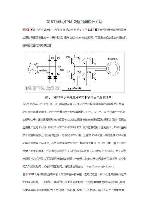
下图是变频空调室外压缩机控制驱动主电路的原理图。
220V交流电压经过由D1~D4和电解电容C1组成的桥式整流和阻容滤波电路后成为给IPM供电的直流电压,六个开关管按照一定规律通断,分别在U、V、W三相输出一系列的矩形信号,通过调整矩形波的频率与占空比达到调节输出电压频率和幅度的目的,即现在应用最广泛的PWM(PULSE WIDTH MODULATE 脉冲宽度调制)控制技术,PWM控制技术从控制思想上可以分成四类:等脉宽PWM法、正弦波PWM法、磁链追踪PWM法和电流追踪型PWM法。
不管采用何种控制方式,都必须注意U、V、W任意一相上下两个桥臂不能同时导通,否则直流电源将在IPM内部形成短路,这是绝对不允许的。
为了避免电源元件的切换反应不及时可能造成的短路,一定要在控制信号之间设定互锁时间,这个时间又叫换流时间,或者叫死区时间。
转载请注明出处:/由于IGBT(绝缘栅极型功率管)等功率器件都存在一定的结电容,所以会造成器件导通关断的延迟现象。
一般在设计电路时已尽量降低该影响,比如尽量提高控制极驱动电压电流,设置结电容释放回路等。
为了使igbt工作可靠,避免由于关断延迟效应造成上下桥臂直通,有必要设置死区时间,也就是上下桥臂同时关断时间。
死区时间可有效地避免延迟效应所造成的一个桥臂未完全关断,而另一桥臂又处于导通状态,避免直通炸模块。
死区时间大,模块工作更加可靠,但会带来输出波形的失真及降低输出效率。
死区时间小,输出波形要好一些,只是会降低可靠性,一般为us级。
一般来说死区时间是不可以改变的,只取决于功率元件制作工艺!死区时间是指控制不到的时间域。
在变频器里一般是指功率器件输出电压、电流的“0”区,在传动控制里一般是指电机正反向转换电压、电流的过零时间。
一种IGBT变频器死区时间的补偿策略
∀UC + ∀U + ∀U + ∀U - ∀U - ∀U - ∀U
∀ Ui ∀ U6 ∀ U4 ∀ U5 ∀ U1 ∀ U3 ∀ U2
表中 ∀ U = T d E d/ T sw
由表 1 知, 当旋转电流矢量位于空间六个
不同区域时, 变频器的输出电压也将损失六个
对应的电压矢量 ∀ U 1~ ∀ U 6。这六个偏差电 压矢量的方向与变频器的六个非零空间电压矢 量方向完全一致, 幅值为 3∀U/ 2。
5结论
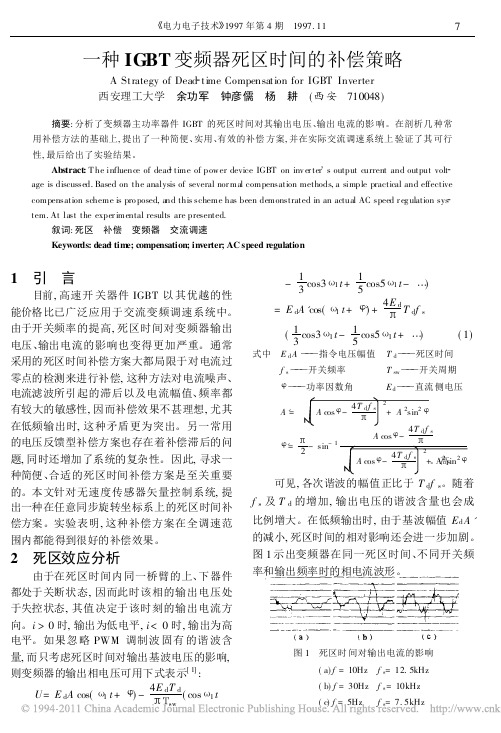
( a) f = 1Hz, f s= 10kHz ( b) f = 40Hz, f s= 10kHz ( c) f = 30Hz f s= 15kHz
参考文献 1 Y. Murai. W av eform Distor tion and Corr ection Cir cuit for PWM Inv er ters with Sw itching Lag times. IEEE IAS 1985: 433~ 441 2 T akashi Sukeg aw a etc. . Fully Digital , Vector controlled P WM V SI fed A C Drives wit h an Inverter Dead time Compensat ion Strateg y. I EEE T rans. on IA,
, 本文提出的死区时间补偿方案简单易 行, 尤其在低频输出时具有很好的补偿效果。
− 由于在同步旋转坐标系上进行补偿 , 对 检测电流的滤波不会引起滞后。
. 对电流采样速度的要求低, 易于软件实
作者简介
1991, 27( 3) : 552~ 558
3 松井 孝 行 等. 电压 制 御形 PW M
正确计算死区时间_英飞凌

AN2007-04 H o w t o c a l c u l a t e a n d m i n i m i z e t h e d e a dt i m e r e q u i r e m e n t f o r I G B T s p r o p e r l yPower Management and DrivesEdition 2008-05-07Published byInfineon Technologies AG81726 München, Germany© Infineon Technologies AG 2008.All Rights Reserved.Attention please!THE INFORMATION GIVEN IN THIS APPLICATION NOTE IS GIVEN AS A HINT FOR THE IMPLEMENTATION OF THE INFINEON TECHNOLOGIES COMPONENT ONLY AND SHALL NOT BE REGARDED AS ANY DESCRIPTION OR WARRANTY OF A CERTAIN FUNCTIONALITY, CONDITION OR QUALITY OF THE INFINEON TECHNOLOGIES COMPONENT. THE RECIPIENT OF THIS APPLICATION NOTE MUST VERIFY ANY FUNCTION DESCRIBED HEREIN IN THE REAL APPLICATION. INFINEON TECHNOLOGIES HEREBY DISCLAIMS ANY AND ALL WARRANTIES AND LIABILITIES OF ANY KIND (INCLUDING WITHOUT LIMITATION WARRANTIES OF NON-INFRINGEMENT OF INTELLECTUAL PROPERTY RIGHTS OF ANY THIRD PARTY) WITH RESPECT TO ANY AND ALL INFORMATION GIVEN IN THIS APPLICATION NOTE.InformationFor further information on technology, delivery terms and conditions and prices please contact your nearest Infineon Technologies Office ().WarningsDue to technical requirements components may contain dangerous substances. For information on the types in question please contact your nearest Infineon Technologies Office.Infineon Technologies Components may only be used in life-support devices or systems with the express written approval of Infineon Technologies, if a failure of such components can reasonably be expected to cause the failure of that life-support device or system, or to affect the safety or effectiveness of that device or system. Life support devices or systems are intended to be implanted in the human body, or to supportand/or maintain and sustain and/or protect human life. If they fail, it is reasonable to assume that the healthAP99007Revision History: 2007-08 V1.0 Previous Version: nonePage Subjects (major changes since last revision)FirstreleaseAuthor: Zhang Xi IFAG AIM PMD ID AETable of Contents Page 1Introduction (5)1.1Reason of IGBT bridge shoot through (5)1.2Impact of dead time on inverter operation (5)2Calculate proper dead time (6)2.1Basics for calculating the dead time (6)2.2Definition of switching and delay times (7)2.3Influence of gate resistor / driver output impedance (8)2.4Impact of other parameters on delay time (9)2.4.1Turn on delay time (9)2.4.2Turn off delay time (10)2.4.3Verification of calculated dead time (12)3How to reduce dead time (13)4Conclusion (14)Bibliography (15)1 IntroductionIn modern industry the voltage source inverter with IGBT devices is used more and more. To ensure proper operation, the bridge shoot through always should be avoided. Bridge shoot through will generate unwanted additional losses or even cause thermal runaway. As a result failure of IGBT devices and whole inverter is possible.1.1 Reason of IGBT bridge shoot throughThe typical configuration of a phase-leg with IGBTs is shown in the following figure. In normal operation two IGBTs will be switched on and off one after the other. Having both devices conducting at the same time will result in a rise of current only limited by DC-link stray inductance.Figure 1 Typical configuration of a voltage source inverterOf course no one will turn on the two IGBTs at the same time on purpose, but since the IGBT is not an ideal switch, turn on time and turn off time are not strictly identical. In order to avoid bridge shoot through it is always recommended to add a so called “interlock delay time” or more popular “dead time” into the control scheme. With this additional time one IGBT will be always turned off first and the other will be turned on after dead time is expired, hence bridge shoot through caused by the unsymmetrical turn on and turn off time of the IGBT devices can be avoided.1.2 Impact of dead time on inverter operationGenerally there are two types of dead time, the first one is control dead time and the second is effective dead time. The control dead time is the dead time, which will be implemented into control algorithms in order to get proper effective dead time at the devices. Target for setting control dead time is to ensure that effective dead time is always positive. Due to the fact that calculation of control dead time is always based on a worst case consideration, an effective dead time being a significant portion of the control dead time will result. Providing dead time can on one side avoid bridge shoot through but on the other side it has also adverse effect. To clarify the effect of dead time, let’s consider one leg of the voltage source inverter as shown in Figure. 2. Assuming first that output current flows in direction shown on the illustration IGBT T1 switches from ON to OFF and IGBT T2 switches from OFF to ON after slight dead time. During effective dead time both devices are off and freewheeling diode D2 is conducting output current. So negative DC link voltage is applied to the output, which is desired here. Consider the other case that T1 switches from OFF to ON and T2 from ON to OFF, then, with current in the same direction D2 still conducts the current during dead time, so that output voltage will be also negative DC link voltage, which is undesired here. The conclusion can besummarized as follows: during effective dead time output voltage is determined by the direction of output current but not the control signal.If we consider output current in the opposite direction than illustrated in figure 2, then we will gain a voltage if T1 switches from ON to OFF and T2 switched from OFF to ON. So in general output voltage and as a result also output current will be distorted with application of a dead time. If we choose a dead time unnecessary large, then in case of an induction motor the system will become instable and may cause some destructive effects [1]. So the process of choosing dead time is very important and should be performed very carefully.CurrentFigure 2One leg of voltage source inverterThis application note will explain how to measure delay time of IGBTs in practice and how to calculate the control dead time properly based on measurements.2 Calculate proper dead timeAs already mentioned, dead time should be chosen on one hand to satisfy the need of avoiding bridge shoot through, on the other hand dead time should be chosen as small as possible to ensure correct operation of voltage source inverter. So a big challenge here is to find out a proper dead time for a dedicated IGBT device and driver.2.1 Basics for calculating the dead timeFor calculation of control dead time we use the following equation:()[]2.1)(______×−+−=MIN PDD MAX PDD MIN ON D MAX OFF D dead t t t t t (1)Where Td_off_max : the maximal turn off delay time. Td_on_min : the minimal turn on delay time.Tpdd_max : the maximal propagation delay of driver. Tpdd_min : the minimum propagation delay of driver.1.2: safety margin to be multiplied.In this equation the first term td_off_max-td_on_min is the difference of the maximal turn off delay time andthe minimal turn on delay time. This term describes characteristic of IGBT device itself plus gate resistor which is used. Since fall and rise time is normally very short in comparison with delay time, they will be not considered here. The other term tpdd_max-tpdd_min is the propagation delay time difference (delay timemismatch) which is determined from driver. This parameter will be found normally in datasheet of driver from driver manufacturers. Typically this value is quiet high with opto-coupler based drivers.Sometimes dead time will be calculated from typical datasheet values just multiplying by a safety factor from field experience. This method will work in some cases but is not precise enough in general. With measurements shown here, a more precise approach will be presented.Because IGBT datasheet only gives typical values for standardized operation condition, it is necessary to obtain the maximal values for dedicated driving condition. For this purpose a series of measurements is done in order to obtain proper value for delay time and then to calculate dead time.switching and delay timesof2.2 DefinitionSince we will talk a lot about switching and delay times, it is necessary to give a clear definition here. Infineon Technologies defines the switching time of IGBT as follows:t d_on: from 10% of Vge to 10% if I c.t r: from 10% of Ic to 90% of I c.t d_off : from 90% of Vge to 90% of I c.t f: from 90% of Ic to 10% of I c.Figure 3 Definition of switching times.2.3 Influence of gate resistor / driver output impedanceThe choice of gate resistor will have significant impact on switching delay time. Generally to say, the larger the resistor is the longer the delay time will be. It is recommended to measure delay time with dedicated gate resistor in application. A typical switching time vs. gate resistor value diagram is shown in the following figures:Figure 4Switching times vs. Rg @25°CAll tests were done with FP40R12KT3 module, gate voltage is -15V/+15V, DC link voltage is 600V and switched current is nominal current of 40A.2.4 Impact of other parameters on delay timeBesides the gate resistor values, there are other parameters having significant impact on delay times: • Collector current.•Gate drive supply voltage.2.4.1 Turn on delay timeTo estimate this relationship, a series of measurements was done. First the dependence of turn on delay time and current was investigated. The results are shown in the next figure:Figure 6 The turn on delay time vs. switched current IcAll tests were done with a FP40R12KT3 module at a DC link voltage of 600V, gate resistor is chosen according to datasheet value.From results above it can be seen that turn on delay time is almost constant with variation of collector current Ic. With -15V/+15V gate voltage turn on delay time will get larger than with 0V/+15V gate voltage [2]. For further calculation of control dead time this variation will be neglected since it is quiet small and provides even additional margin.2.4.2 Turn off delay timeThe most important factor in the calculation of dead time is the maximal turn off delay time. Since this value determines almost entirely how long the final calculated dead time will be. So we will investigate this delay time in detail.In order to obtain the maximum turn off delay time following considerations have to be done:1. What and how long is the turn on delay time caused by IGBT device itself?To answer this question the following test based on a characterization driver board is done in laboratory. The characterization driver board is considered as an optimal driver, which means that this particular driver will cause no delay (which is almost true with an oversized driver), so the whole delay time is considered to be caused by the IGBT device itself. Following block diagram shows test setup:Figure 7 Block diagram of test with ideal driver2. What is the maximal turn off delay time if the threshold voltage of IGBT has the minimal value in datasheets? (this reflects the tolerance of Vth from module to module)To answer this question an additional diode is connected to simulate the reduced Vth voltage. The diode has a voltage drop of approximately 0.7…0.8V, which is quite similar to the Vth variation of FP40R12KT3 module. Following block diagram shows principle test setup:Figure 8 Block diagram of the test to simulate variation of Vth in worst case.3. What is the impact of driver output stage on switching times?To answer this concrete question the drivers on the market were splitted into two categories, one with mosfet transistor output stage and the other one with bipolar transistor output stage. For each category separate measurements were made.To simulate drivers with mosfet output stage, another additional resistor was connected and has been considered as the on state resistor Rds(on) of Mosfet transistor. The diode for simulation of Vth variation remained. The following block diagram shows the principle test setup:Figure 9 Block diagram of test to simulate variation of Vth and driver with mosfet output.4. What is the impact of the driver with bipolar transistor output stage?To answer the question an additional diode which simulated the voltage drop on bipolar transistor within output stage was connected. The following block diagram shows principle test setup:Figure 10 Block diagram of the test to simulate the variation of Vth and driver with bipolar transistor outputWith the configurations shown above the measurement of turn off delay time was done in our laboratory with module FP40R12KT3 and driver board which had been considered as optimal. Test conditions were Vdc=600V, Rg=27Ω. Results are shown in the next two figures:Figure 11 Turn off delay time vs. Ic @25°CFigure 12 Turn off delay time vs. Ic @125°CFrom the results we can see that there is a significant increase of turn off delay time with decrease of the switched current Ic. So just simply calculate dead time according to a chosen gate resistor is obviously not precise enough. Measuring the delay time under the dedicated driving condition then calculating dead time according to these values is a better and more precise way. Normally measurement until 1% of the nominal current would be enough to give a sufficient overview for calculating required dead time.Another point to be considered here is that the turn off delay time will increase with 0V/+15V gate drive, and the impact of output stage on switching times will be bigger with 0V/+15V switching. This means that with 0V/+15V switching voltage special care has to be taken by choosing the driver. Additionally, the increase of td_off with lower switched collector current Ic should be considered also.As an example: the HCPL-3120 driver IC will be considered here. This driver IC has a Mosfet output stage for switching off. From diagrams above we can read the value for td_off under 0V/+15V switching condition is roughly 1500ns. The td_on in this case is about 100ns. The tpdd_max-tpdd_min of this driver IC according to datasheet is 700ns. Applying these values to the formula (1) results in a dead time of about 2.5µs.2.4.3 Verification of calculated dead timeWith the discussion above and the formula (1) given in chapter 2.1 it is now possible to calculate the required dead time based on the measurements above. With the calculated dead time, a worst case measurement can then be performed to verify if the chosen dead time is enough or not.From the measurement it can be seen that the turn off delay time increases with temperature. From this reason it is preferable that the test should be done both at cold and hot condition.The schematic illustration of the test looks like following:Figure 13 Schematic illustration of test to check calculated dead time valueThe bottom IGBT has to be switched on and off, then the same for the top one. The time between the two pulses should be adjusted to be the value of calculated dead time for the dedicated driving condition. The negative dc-link current can then be measured and if the dead time is sufficient, a shoot through current should not be observed.Since there is no current through both IGBT, the described test represents the worst case condition for dead time calculation. From the discussion of turn off delay time it is known that dead time will be longer with decrease of collector current, so in case there flows no current, turn off delay time should be largest, which leads to a need of largest dead time. If there is no shoot through current at zero collector current then the chosen dead time is for dedicated driving condition sufficient.3 How to reduce dead timeFor a proper calculation of control dead time the dedicated driving condition should be considered: •What is the applied gate voltage to the IGBT?•What is the chosen gate resistor value?•What type of output stage does the driver have?Based on these conditions a test should be made, from the test results the control dead time can then be calculated using equition (1).Since dead time has a negative impact on the performance of inverter, it has to be minimized. Several methods can be taken.•Take a driver strong enough to sink or source the peak IGBT gate current.•Use negative power supply to accelerate turn off.•Prefer drivers based on fast signal transmission technology like Coreless Transformer Technology to drivers based on traditional opto-coupler technology.•If 0V/15V gate drive is used then consider use of separate Rgon/Rgoff resistor as described below.From measurements shown in chapter 2.3 a very strong dependence of Td_off and gate resistor value can be observed. If the Rgoff reduced then the td_off will be reduced as well as dead time. Infineon suggests reducing the Rgoff to 1/3 of the Rgon value if 0V/15V gate voltage is used. One possible circuit for separate Rgon and Rgoff is as follows:Figure 14 Suggested circuit with 0V/15V gate voltage.R1 should be chosen to satisfy the following relation:)(31int int 11g gon g gongon R R R R R R R +⋅=++⋅(2)int int 1221g gon g gon gon R R R R R R +−⋅⋅==>(3)From equation (3) it is to be noticed that the requirement Rgon>2Rgint has to be fulfilled to get a positivevalue of R1. However, with some modules this requirement can not be true. In this case, R1 can be omitted completely.The diode should be a schottky type diode.Another very important issue with 0V/15V gate voltage is the parasitic turn on effect. This issue can be also solved if suggested circuit is used. For more details on parasitic turn on please refer to AN2006-01[2].4 ConclusionIn this application note an approach of measuring switching times of IGBT and then calculating the control dead time is introduced. First dependence of switching time on gate resistor value was shown, and then influence of gate driver and collector current on switching times was discussed. Finally possible methods to reduce dead time were introduced.Bibliography[1] D.Grahame Holmes, Thomas A. Lipo: …Pulse width modulation for power converters: principles andpractice“, IEEE Press, 2003. ISBN 0-471-20814-0[2] Driving IGBTs with unipolar gate voltage./dgdl/an-2006-01_Driving_IGBTs_with_unipolar_gate_voltage.pdf?folderId=db3a304412b407950112b408e8c9000 4&fileId=db3a304412b407950112b40ed1711291。
- 1、下载文档前请自行甄别文档内容的完整性,平台不提供额外的编辑、内容补充、找答案等附加服务。
- 2、"仅部分预览"的文档,不可在线预览部分如存在完整性等问题,可反馈申请退款(可完整预览的文档不适用该条件!)。
- 3、如文档侵犯您的权益,请联系客服反馈,我们会尽快为您处理(人工客服工作时间:9:00-18:30)。
IGBT(IPM)死区时间的设计方法
1 基本原理推导
①IGBT及光耦开关时间的定义
IGBT开关时间定义光耦开关时间定义
②主电路构成
③逻辑上的死区时间与IGBT端子(C、E)死区时间的关系
下图给出了控制信号、驱动板输出电压和IGBT
端子(C、E)间电压的相位关系。
各延迟时间分别定义为:
t1:开通控制信号-驱动板开通电压信号输出的
延迟时间
t2:驱动板开通电压-IGBT开通输出延迟时间
t3:关断控制信号-驱动板关断电压信号输出的
延迟时间
t4:驱动板关断电压-IGBT关断输出延迟时间
(这里不考虑上下桥臂的差别)
逻辑上设定的死区时间(TD)与IGBT端子(C、
E)死区时间(TD’)的关系如下式。
TD'=TD-(t3+t4)+(t1+t2) (1)
因此逻辑上的死区时间(TD)随延迟时间
t1~t4的大小而变化成实际的死区时间(TD
')。
下面分别推导驱动板的延时 (t1、t3)和IGBT延时(t2、t4)。
2 关于死区时间的设计方法
对式TD'=TD-(t3+t4)+(t1+t2)进行变换得
TD=TD'+(t3+t4)-(t1+t2)= TD'+(t3- t1)+(t4-t2)
剩下就是如何界定驱动板的延时 (t1、t3)和IGBT 延时(t2、t4)。
设计方法就是分为这两部分进行设计的,分别IGBT 部分的死区时间和HIC 部分的死区时间。
(1)IGBT 部分的死区时间
①IGBT 开关时间的误差数据的收集及最大误差数据的算出
根据各个公司的IGBT 数据,算出IGBT 开关时间的误差数据(Tj =25℃)。
根据σ及X ±4σ计算各IGBT 的X ±4σ.(误差最大)以下给出富士IGBT 的σ值供参考. ○
600V 系列 σ=0.041(最大) ○1200V 系列 σ=0.063(最大)
②结温为25℃和125℃时的开关时间比率计算
根据数据手册中的结温在25℃和125℃、电流为额定电流时的开关时间(ton,toff),计算温升比率(T125/T25)。
开关时间T(uS) 器件额定电流 符号 结温 Tj=125℃
时倍率 Min 值
Typ 值
Max 值 25 0.512 (typ-4σ)0.764 1.016
(typ+4σ) Ton
125
1.111 0.568 0.849 1.129 25 0.723 0.975 1.227 1MBI300N-120 Toff
125
1.474
1.065
1.437
1.808
※σ为富士推荐的最大值0.063。
③结温为125℃时的开关时间计算
由①和②的结果,两者相乘,可以计算出结温为125℃时的开关时间。
④驱动条件时Rg,Vge 的比率计算
由于数据手册中给出的数据的条件(Rg,Vge)与实际变频器驱动的条件不同,因此需要计算实际IGBT 驱动条件下的开关时间比率。
⑤修正开关时间的计算
从4的结果可以及③的结果可以计算出考虑这些比率时结温为125℃时的开关时间。
然后可
以分别求出ton、toff 的min 值,typ 值和max 值。
开关时间T(uS) 器件额定电流 符号 结温 Rg (Ω)Rg 倍率 Vge 倍率 Min 值 Typ 值 Max 值 Ton
125 1.205 0.828 0.567 0.847 1.126 1MBI300N-120 Toff
125
3.9
1.338
1.143
1.622
2.189
2.755
这里Rg、-Vge 的倍率是通过Rg-Ton、Toff 及-Vge 与Ton、Toff 的特性曲线求得。
从上表1得到的数据乘以这两个倍率即得本表的数据,如0.568×1.205×0.828=0.567。
⑥IGBT 死区时间的计算
从⑤的开关时间中可以求出toff(max)-ton(min),至此IGBT 部的死区时间已经求出。
使用器件 Rg(Ω) toff(max)(uS) ton(min)(uS)Td(IGBT)(uS)1MBI300N-120 3.9
2.755
0.567
2.188
(2)驱动板部HIC 死区时间的设计方法
① 周围温度25℃与最大温度时的开关时间的计算
以M57962AL
为例说明,其各温度时的开关时间数据如下表。
开关时间T(uS) 驱动IC 符号 动作环境温度 Min 值 Typ 值 Max 值 25 0.3 0.5 1.0 TPLH 60 0.3 0.849 1.129 25 1.0 1.3 M57962AL
TPHL
60
1.5
②驱动板部HIC 死区时间的设计
环境温度为60℃时的死区时间为Td(HIC)=tpHL(max)- tpLH(min) 故根据上面的数据,计算得Td(HIC)=1.5- 0.3=1.2(uS)
(3)全死区时间的计算
当计算出IGBT 部分的死区时间和HIC 部分的死区时间后,全死区时间就可以计算出来了。
TD=[tpHL(max)- tpLH(min)]+[toff(max)-ton(min)]
使用模块
使用驱动芯片 INV容量
(KW)
IGBT死区时间
Td(IGBT)(uS)
HIC死区时间
Td(HIC)(uS)
全死区时间
Td (uS)
1MBI300N-120
M57962AL
75 2.188 1.20 3.388。