半导体导论翻译
半导体制程技术导论Chapter_1导论
石英基板 光刻工艺:借助光刻胶将印在掩膜上的图形结构转移到硅片表面 光刻胶:批光照后能具有抗蚀能力的高分子化合物,用于在半导 体基件表面产生电路的形状。 正光刻胶:受光照部分发生降解反应而能为显影液所溶解。留下 的非曝光部分的图形与掩模版一致。 负光刻胶:受光照部分产生交链反应而成为不溶物,非曝光部分 22 被显影液溶解,获得的图形与掩模版图形互补。
2
目标
读完本章之后,你应该能够:
• • • •
熟悉半导体相关术语的使用 描述基本的集成电路制造流程 简明的解释每一个制程步骤 将你的工作或制造产品与半导体制造工艺 相结合,并建立它们之间的联系
3
主题
• • • • 简介 集成电路组件和设计 半导体制程 未来的走向
4
简介
• • • • • 第一个晶体管,AT&T贝尔实验室, 1947 第一个单晶锗, 1950 第一个单晶硅, 1952 第一个集成电路组件, 德州仪器, 1958 第一个硅集成电路芯片, 费尔查德照相机 公司, 1961
半导体制程技术导论 Chapter 1导论
王红江, Ph. D. fwang@ 江苏科技大学
1
参考书籍
• Hong Xiao. Introduction to Semiconductor Manufacturing Technology. SPIE. 2012 • 萧宏. 半导体制造技术导论. 电子工业出版社, 2012 • 施敏. 半导体器件物理与工艺. 苏州大学出版社, 2002 • Peter Van Zant. 芯片制造——半导体工艺制程实用 教程. 电子工业出版社 • Michael Quirk, Julian Serda. 半导体制造技术. 电子 工业出版社. 2009
《半导体光电子学课件》中文翻译.doc
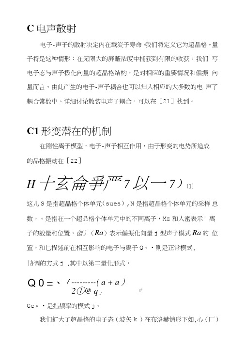
C电声散射电子-声子的散射决定内在载流子寿命。
我们将定义它为超晶格。
量子将是这种情形:在无限大的屏蔽浓度中捕获到有限的收获。
我们写电子态与声子极化向量的超晶格结构,是对相应的重要情况和偏振向量而言。
由此产生的电子-声子耦合也可以归入相应的大多数的电声了耦合常数中。
详细讨论散装电声子耦合,可以在[21]找到。
C1形变潜在的机制在刚性离子模型,电子-声子相互作用,由于形变的电势所造成的品格振动在[22]H十玄侖爭严7以一7)⑴这儿S是指超晶格个体单元(sues),N是指超晶格个体单元的采样总数,。
是指在一个超品格个体单元中的不同离子,Mz和人密表示" 离子的数量和位置,创)(Ra)表示偏振化向量j型声子模式Ra的位置,和匕描述前在相互影响的电子与离子Q。
•则是正常模式,协调的方式j,其中以第二量化形式,Q 0 =、/ --------- ( a + a )2①@ q」qjGe〃•是指频率的模式j。
我们扩大了超晶格的电子态(波矢k )在布洛赫情形下如,心(厂)是个例子,V表示和大部分相关。
瓦(厂)=工心(“也)%”(厂) 这儿心定义为在大多数情况下保持不变。
这里g.,・指的是z 组成的超 晶格倒数矢量。
矩阵元的H" 之间的两个电子态与波向量k 和F 是 nj Eg ,3s7nD 九 lq + g ②这儿% ⑷三J 〃3厂%(沪/,2)0心心)这儿匕皿指的是°邙口离子或阴离子)的组成部分,偏振波矢量q 的大部分模式V 和Mg 〃总质量的绝大多数晶胞都在相应的大部分材 料中。
当中的+(-)符号表示上述方程的声子吸收(释放)过程。
注 意,在EQN(3)中的Dv,v (q )仅仅是对于大多数材料的电声了耦合常 数而言。
为光学声子中心附近区域D (q )的q 近似为独立的。
而对于声 学模式,D (q )是成正比的q,与相称常数被称为形变机制。
C2极性光散射由< 約 H el _ph | k >=-———s2 叫 NM cellqHx对于III-V型半导体,光学声子促进了材料中的大多数单元的离子间的相互运动,从而导致了偶级子震荡。
半导体专业名词解释
Cd cadmium
AWS advanced wet station
Manufacturing and Science
Sb antimony
===B===
B billion; boron
Ba barium
BARC bottom antireflective coating
BASE Boston Area Semiconductor Education (Council)
ACF anisotropic conductive film
ACI after-clean inspection
ACP anisotropic conductive paste
ACT alternative control techniques; actual cycle time
Al aluminum
ALD atomic layer deposition
ALE atomic layer epitaxy; application logic element
ALS advanced light source; advanced low-power Schottky
===A===
A/D analog to digital
AA atomic absorption
AAS atomic absorption spectroscopy
ABC activity-based costing
ABM activity-based management
AC alternating current; activated carbon
半导体物理与器件——Terms汉译英.docx

半导体物理与器件--- Terms(术语)U1 Terms:Semic on ductor physics and devices 半导体物理与器件,Space lattice 空间晶格'unit cell 晶胞'primitive cell 原胞,basic crystal structures 基本晶格结构(five), Miller indices 密勒指数' atomic bonding 原子价键U2 Terms:quantum mechanics 量了力学'energy quanta 能量子,wave-particle duality 波粒二象性,the uncertainty principle测不准原理/海森堡不确定原理Schrodinger's wave equation 薛定灣波动方程,eletrons in free Space 自由空间中的电子the infinite potential well 无限深势阱,the step potential function 阶跃势函数,the potential barrier 势垒.U3 Terms:Pauli exclusion principle 泡利不相容原理,quantum state 量了态. allowed energy band 允带'forbidden energy band 禁带. con ducti on band 导带'vale nee band 价带,hole 空穴'electron 电子.effective mass 有效质量.density of states function 状态密度函数,the Fermi-Dirac probability function 费米■狄拉克概率函数' the Boltzmann approximation 波尔兹曼近彳以‘ the Fermi energy 费米能级.U4 Terms:charge carriers 载流子'effective density of states function 有效族犬态密度函数,intrinsic 本征的,the intrinsic carrier concentration 本征载流子浓度'the intrinsic Fermi level 本征费米能级.charge n eutrality 电中性状态'compe nsated semic on ductor 补偿半导体‘ degenerate 简并的,non-degenerate 非简并的'position of E F费米能级的位置U5 Terms:drift current 漂移电流,diffusion current 扩散电流,mobility 迁移率,lattice scattering 晶格散身寸,ionized impurity scattering 电离杂质散射'velocity saturation饱和速度’conductivity 电导率‘resistivity 电阻率.graded impurity distribution 杂质梯度分布'the induced electric field 感生电场'the Einstein relation 爱因斯坦关系, the hall effect 霍尔效应U6 Terms:non equilibrium excess carriers 非平衡过剩载流子'carrier generation and recombination 载流子的产生与复合'excess minority carrier 过剩少子,lifetime 寿命'low-level injection 小注入,ambipolar transport 双极输运'quasi-Fermi energy 准费米能级.U7 Terms:the space charge region 空间电荷区'the built-in potential 内建电势,the built-in potential barrier 内建电势差,the space charge width 空间电荷区宽度,zero applied bias 零偏压,reverse applied bias 反偏'on esided jun ction 单边突变结.U8 Terms:the PN junction diode PN 结二极管,minority carrier distribution 少数载流子分布'the ideal-diode equation 理想二极管方程,the reverse saturation current density 反向饱和电流密度.a short diode 短二极管,generation-recombination current 产生・复合电流,the Zener effect 齐纳效应,the avalanche effect 雪崩效应,breakdown 击穿.U9 Terms:Schottky barrier diode (SBD)肖特基势垒二极管,Schottky barrier height 肖特基势垒高度.Ohomic contact 欧姆接触'heterojunction 异质纟吉'homojunction 单质纟吉,turn-on voltage 开启电压,narrow-bandgap 窄带隙'wide-bandgap 宽带隙,2-D electron gas 二维电子气U10 Terms:bipolar transistor 双极晶体管,base基极,emitter发射极,collector集电极. forward active regi on 正向有源区'in verse active region 反向有源区' cut-off 截止,saturation 饱和,current gain电流增益'common・base 共基,commorvemitter 共身寸.base width modulation 基区宽度调制效应,Early effect 厄利效应'Early voltage厄利电压Ull Terms:Gate 栅极,source 源极,drain 漏极'substrate 基底. work function difference 功函数差threshold voltage 阈值电压'flat-band voltage 半带电压enhancement mode 增强型'depletion mode 耗尽型strong inversion 强反型'weak inversion 弱反型,transconductance 跨导'l-V relationship 电流■电压关系。
半导体词典
Abrupt junction 突变结Accelerated testing 加速实验Acceptor 受主Acceptor atom 受主原子Accumulation 积累、堆积Accumulating contact 积累接触Accumulation region 积累区Accumulation layer 积累层Active region 有源区Active component 有源元Active device 有源器件Activation 激活Activation energy 激活能Active region 有源(放大)区Admittance 导纳Allowed band 允带Alloy-junction device合金结器件Aluminum(Aluminium) 铝Aluminum – oxide 铝氧化物Aluminum passivation 铝钝化Ambipolar 双极的Ambient temperature 环境温度Amorphous 无定形的,非晶体的Amplifier 功放扩音器放大器Analogue(Analog) comparator 模拟比较器Angstrom 埃Anneal 退火Anisotropic 各向异性的Anode 阳极Arsenic (AS) 砷Auger 俄歇Auger process 俄歇过程Avalanche 雪崩Avalanche breakdown 雪崩击穿Avalanche excitation雪崩激发Background carrier 本底载流子Background doping 本底掺杂Backward 反向Backward bias 反向偏置Ballasting resistor 整流电阻Ball bond 球形键合Band 能带Band gap 能带间隙Barrier 势垒Barrier layer 势垒层Barrier width 势垒宽度Base 基极Base contact 基区接触Base stretching 基区扩展效应Base transit time 基区渡越时间Base transport efficiency基区输运系数Base-width modulation基区宽度调制Basis vector 基矢Bias 偏置Bilateral switch 双向开关Binary code 二进制代码Binary compound semiconductor 二元化合物半导体Bipolar 双极性的Bipolar Junction Transistor (BJT)双极晶体管Bloch 布洛赫Blocking band 阻挡能带Blocking contact 阻挡接触Body - centered 体心立方Body-centred cubic structure 体立心结构Boltzmann 波尔兹曼Bond 键、键合Bonding electron 价电子Bonding pad 键合点Bootstrap circuit 自举电路Bootstrapped emitter follower 自举射极跟随器Boron 硼Borosilicate glass 硼硅玻璃Boundary condition 边界条件Bound electron 束缚电子Breadboard 模拟板、实验板Break down 击穿Break over 转折Brillouin 布里渊Brillouin zone 布里渊区Built-in 内建的Build-in electric field 内建电场Bulk 体/体内Bulk absorption 体吸收Bulk generation 体产生Bulk recombination 体复合Burn - in 老化Burn out 烧毁Buried channel 埋沟Buried diffusion region 隐埋扩散区Can 外壳Capacitance 电容Capture cross section 俘获截面Capture carrier 俘获载流子Carrier 载流子、载波Carry bit 进位位Carry-in bit 进位输入Carry-out bit 进位输出Cascade 级联Case 管壳Cathode 阴极Center 中心Ceramic 陶瓷(的)Channel 沟道Channel breakdown 沟道击穿Channel current 沟道电流Channel doping 沟道掺杂Channel shortening 沟道缩短Channel width 沟道宽度Characteristic impedance 特征阻抗Charge 电荷、充电Charge-compensation effects 电荷补偿效应Charge conservation 电荷守恒Charge neutrality condition 电中性条件Charge drive/exchange/sharing/transfer/storage 电荷驱动/交换/共享/转移/存储Chemmical etching 化学腐蚀法Chemically-Polish 化学抛光Chemmically-Mechanically Polish (CMP) 化学机械抛光Chip 芯片Chip yield 芯片成品率Clamped 箝位Clamping diode 箝位二极管Cleavage plane 解理面Clock rate 时钟频率Clock generator 时钟发生器Clock flip-flop 时钟触发器Close-packed structure 密堆积结构Close-loop gain 闭环增益Collector 集电极Collision 碰撞Compensated OP-AMP 补偿运放Common-base/collector/emitter connection 共基极/集电极/发射极连接Common-gate/drain/source connection 共栅/漏/源连接Common-mode gain 共模增益Common-mode input 共模输入Common-mode rejection ratio (CMRR) 共模抑制比Compatibility 兼容性Compensation 补偿Compensated impurities 补偿杂质Compensated semiconductor 补偿半导体Complementary Darlington circuit 互补达林顿电路Complementary Metal-Oxide-Semiconductor Field-Effect-Transistor(CMOS)互补金属氧化物半导体场效应晶体管Complementary error function 余误差函数Computer-aided design (CAD)/test(CAT)/manufacture(CAM) 计算机辅助设计/ 测试/制造Compound Semiconductor 化合物半导体Conductance 电导Conduction band (edge) 导带(底) Conduction level/state 导带态Conductor 导体Conductivity 电导率Configuration 组态Conlomb 库仑Conpled Configuration Devices 结构组态Constants 物理常数Constant energy surface 等能面Constant-source diffusion恒定源扩散Contact 接触Contamination 治污Continuity equation 连续性方程Contact hole 接触孔Contact potential 接触电势Continuity condition 连续性条件Contra doping 反掺杂Controlled 受控的Converter 转换器Conveyer 传输器Copper interconnection system 铜互连系统Couping 耦合Covalent 共阶的Crossover 跨交Critical 临界的Crossunder 穿交Crucible坩埚Crystal defect/face/orientation/lattice 晶体缺陷/晶面/晶向/晶格Current density 电流密度Curvature 曲率Cut off 截止Current drift/dirve/sharing 电流漂移/驱动/共享Current Sense 电流取样Curvature 弯曲Custom integrated circuit 定制集成电路Cylindrical 柱面的Czochralshicrystal 直立单晶Czochralski technique 切克劳斯基技术(Cz法直拉晶体J)Dangling bonds 悬挂键Dark current 暗电流Dead time 空载时间Debye length 德拜长度De.broglie 德布洛意Decderate 减速Decibel (dB) 分贝Decode 译码Deep acceptor level 深受主能级Deep donor level 深施主能级Deep impurity level 深度杂质能级Deep trap 深陷阱Defeat 缺陷Degenerate semiconductor 简并半导体Degeneracy 简并度Degradation 退化Degree Celsius(centigrade) /Kelvin 摄氏/开氏温度Delay 延迟Density 密度Density of states 态密度Depletion 耗尽Depletion approximation 耗尽近似Depletion contact 耗尽接触Depletion depth 耗尽深度Depletion effect 耗尽效应Depletion layer 耗尽层Depletion MOS 耗尽MOSDepletion region 耗尽区Deposited film 淀积薄膜Deposition process 淀积工艺Design rules 设计规则Die 芯片(复数dice)Diode 二极管Dielectric 介电的Dielectric isolation 介质隔离Difference-mode input 差模输入Differential amplifier 差分放大器Differential capacitance 微分电容Diffused junction 扩散结Diffusion 扩散Diffusion coefficient 扩散系数Diffusion constant 扩散常数Diffusivity 扩散率Diffusion capacitance/barrier/current/furnace 扩散电容/势垒/电流/炉Digital circuit 数字电路Dipole domain 偶极畴Dipole layer 偶极层Direct-coupling 直接耦合Direct-gap semiconductor 直接带隙半导体Direct transition 直接跃迁Discharge 放电Discrete component 分立元件Dissipation 耗散Distribution 分布Distributed capacitance 分布电容Distributed model 分布模型Displacement 位移Dislocation 位错Domain 畴Donor 施主Donor exhaustion 施主耗尽Dopant 掺杂剂Doped semiconductor 掺杂半导体Doping concentration 掺杂浓度Double-diffusive MOS(DMOS)双扩散MOS.Drift 漂移Drift field 漂移电场Drift mobility 迁移率Dry etching 干法腐蚀Dry/wet oxidation 干/湿法氧化Dose 剂量Duty cycle 工作周期Dual-in-line package (DIP)双列直插式封装Dynamics 动态Dynamic characteristics 动态属性Dynamic impedance 动态阻抗Early effect 厄利效应Early failure 早期失效Effective mass 有效质量Einstein relation(ship) 爱因斯坦关系Electric Erase Programmable Read Only Memory(E2PROM) 一次性电可擦除只读存储器Electrode 电极Electrominggratim 电迁移Electron affinity 电子亲和势Electronic -grade 电子能Electron-beam photo-resist exposure 光致抗蚀剂的电子束曝光Electron gas 电子气Electron-grade water 电子级纯水Electron trapping center 电子俘获中心Electron Volt (eV) 电子伏Electrostatic 静电的Element 元素/元件/配件Elemental semiconductor 元素半导体Ellipse 椭圆Ellipsoid 椭球Emitter 发射极Emitter-coupled logic 发射极耦合逻辑Emitter-coupled pair 发射极耦合对Emitter follower 射随器Empty band 空带Emitter crowding effect 发射极集边(拥挤)效应Endurance test =life test 寿命测试Energy state 能态Energy momentum diagram 能量-动量(E-K)图Enhancement mode 增强型模式Enhancement MOS 增强性MOS Entefic (低)共溶的Environmental test 环境测试Epitaxial 外延的Epitaxial layer 外延层Epitaxial slice 外延片Expitaxy 外延Equivalent curcuit 等效电路Equilibrium majority /minority carriers 平衡多数/少数载流子Erasable Programmable ROM (EPROM)可搽取(编程)存储器Error function complement 余误差函数Etch 刻蚀Etchant 刻蚀剂Etching mask 抗蚀剂掩模Excess carrier 过剩载流子Excitation energy 激发能Excited state 激发态Exciton 激子Extrapolation 外推法Extrinsic 非本征的Extrinsic semiconductor 杂质半导体Face - centered 面心立方Fall time 下降时间Fan-in 扇入Fan-out 扇出Fast recovery 快恢复Fast surface states 快界面态Feedback 反馈Fermi level 费米能级Fermi-Dirac Distribution 费米-狄拉克分布Femi potential 费米势Fick equation 菲克方程(扩散)Field effect transistor 场效应晶体管Field oxide 场氧化层Filled band 满带Film 薄膜Flash memory 闪烁存储器Flat band 平带Flat pack 扁平封装Flicker noise 闪烁(变)噪声Flip-flop toggle 触发器翻转Floating gate 浮栅Fluoride etch 氟化氢刻蚀Forbidden band 禁带Forward bias 正向偏置Forward blocking /conducting正向阻断/导通Frequency deviation noise频率漂移噪声Frequency response 频率响应Function 函数Gain 增益Gallium-Arsenide(GaAs) 砷化钾Gamy ray r 射线Gate 门、栅、控制极Gate oxide 栅氧化层Gauss(ian)高斯Gaussian distribution profile 高斯掺杂分布Generation-recombination 产生-复合Geometries 几何尺寸Germanium(Ge) 锗Graded 缓变的Graded (gradual) channel 缓变沟道Graded junction 缓变结Grain 晶粒Gradient 梯度Grown junction 生长结Guard ring 保护环Gummel-Poom model 葛谋-潘模型Gunn - effect 狄氏效应Hardened device 辐射加固器件Heat of formation 形成热Heat sink 散热器、热沉Heavy/light hole band 重/轻空穴带Heavy saturation 重掺杂Hell - effect 霍尔效应Heterojunction 异质结Heterojunction structure 异质结结构Heterojunction Bipolar Transistor(HBT)异质结双极型晶体High field property 高场特性High-performance MOS.( H-MOS)高性能MOS. Hormalized 归一化Horizontal epitaxial reactor 卧式外延反应器Hot carrior 热载流子Hybrid integration 混合集成Image - force 镜象力Impact ionization 碰撞电离Impedance 阻抗Imperfect structure 不完整结构Implantation dose 注入剂量Implanted ion 注入离子Impurity 杂质Impurity scattering 杂志散射Incremental resistance 电阻增量(微分电阻)In-contact mask 接触式掩模Indium tin oxide (ITO) 铟锡氧化物Induced channel 感应沟道Infrared 红外的Injection 注入Input offset voltage 输入失调电压Insulator 绝缘体Insulated Gate FET(IGFET)绝缘栅FET Integrated injection logic集成注入逻辑Integration 集成、积分Interconnection 互连Interconnection time delay 互连延时Interdigitated structure 交互式结构Interface 界面Interference 干涉International system of unions国际单位制Internally scattering 谷间散射Interpolation 内插法Intrinsic 本征的Intrinsic semiconductor 本征半导体Inverse operation 反向工作Inversion 反型Inverter 倒相器Ion 离子Ion beam 离子束Ion etching 离子刻蚀Ion implantation 离子注入Ionization 电离Ionization energy 电离能Irradiation 辐照Isolation land 隔离岛Isotropic 各向同性Junction FET(JFET) 结型场效应管Junction isolation 结隔离Junction spacing 结间距Junction side-wall 结侧壁Latch up 闭锁Lateral 横向的Lattice 晶格Layout 版图Lattice binding/cell/constant/defect/distortion 晶格结合力/晶胞/晶格/晶格常熟/晶格缺陷/晶格畸变Leakage current (泄)漏电流Level shifting 电平移动Life time 寿命linearity 线性度Linked bond 共价键Liquid Nitrogen 液氮Liquid-phase epitaxial growth technique 液相外延生长技术Lithography 光刻Light Emitting Diode(LED) 发光二极管Load line or Variable 负载线Locating and Wiring 布局布线Longitudinal 纵向的Logic swing 逻辑摆幅Lorentz 洛沦兹Lumped model 集总模型Majority carrier 多数载流子Mask 掩膜板,光刻板Mask level 掩模序号Mask set 掩模组Mass - action law质量守恒定律Master-slave D flip-flop主从D触发器Matching 匹配Maxwell 麦克斯韦Mean free path 平均自由程Meandered emitter junction梳状发射极结Mean time before failure (MTBF) 平均工作时间Megeto - resistance 磁阻Mesa 台面MESFET-Metal Semiconductor金属半导体FETMetallization 金属化Microelectronic technique 微电子技术Microelectronics 微电子学Millen indices 密勒指数Minority carrier 少数载流子Misfit 失配Mismatching 失配Mobile ions 可动离子Mobility 迁移率Module 模块Modulate 调制Molecular crystal分子晶体Monolithic IC 单片IC MOSFET金属氧化物半导体场效应晶体管Mos. Transistor(MOST )MOS. 晶体管Multiplication 倍增Modulator 调制Multi-chip IC 多芯片ICMulti-chip module(MCM) 多芯片模块Multiplication coefficient倍增因子Naked chip 未封装的芯片(裸片)Negative feedback 负反馈Negative resistance 负阻Nesting 套刻Negative-temperature-coefficient 负温度系数Noise margin 噪声容限Nonequilibrium 非平衡Nonrolatile 非挥发(易失)性Normally off/on 常闭/开Numerical analysis 数值分析Occupied band 满带Officienay 功率Offset 偏移、失调On standby 待命状态Ohmic contact 欧姆接触Open circuit 开路Operating point 工作点Operating bias 工作偏置Operational amplifier (OPAMP)运算放大器Optical photon =photon 光子Optical quenching光猝灭Optical transition 光跃迁Optical-coupled isolator光耦合隔离器Organic semiconductor有机半导体Orientation 晶向、定向Outline 外形Out-of-contact mask非接触式掩模Output characteristic 输出特性Output voltage swing 输出电压摆幅Overcompensation 过补偿Over-current protection 过流保护Over shoot 过冲Over-voltage protection 过压保护Overlap 交迭Overload 过载Oscillator 振荡器Oxide 氧化物Oxidation 氧化Oxide passivation 氧化层钝化Package 封装Pad 压焊点Parameter 参数Parasitic effect 寄生效应Parasitic oscillation 寄生振荡Passination 钝化Passive component 无源元件Passive device 无源器件Passive surface 钝化界面Parasitic transistor 寄生晶体管Peak-point voltage 峰点电压Peak voltage 峰值电压Permanent-storage circuit 永久存储电路Period 周期Periodic table 周期表Permeable - base 可渗透基区Phase-lock loop 锁相环Phase drift 相移Phonon spectra 声子谱Photo conduction 光电导Photo diode 光电二极管Photoelectric cell 光电池Photoelectric effect 光电效应Photoenic devices 光子器件Photolithographic process 光刻工艺(photo) resist (光敏)抗腐蚀剂Pin 管脚Pinch off 夹断Pinning of Fermi level 费米能级的钉扎(效应)Planar process 平面工艺Planar transistor 平面晶体管Plasma 等离子体Plezoelectric effect 压电效应Poisson equation 泊松方程Point contact 点接触Polarity 极性Polycrystal 多晶Polymer semiconductor聚合物半导体Poly-silicon 多晶硅Potential (电)势Potential barrier 势垒Potential well 势阱Power dissipation 功耗Power transistor 功率晶体管Preamplifier 前置放大器Primary flat 主平面Principal axes 主轴Print-circuit board(PCB) 印制电路板Probability 几率Probe 探针Process 工艺Propagation delay 传输延时Pseudopotential method 膺势发Punch through 穿通Pulse triggering/modulating 脉冲触发/调制Pulse Widen Modulator(PWM) 脉冲宽度调制Punchthrough 穿通Push-pull stage 推挽级Quality factor 品质因子Quantization 量子化Quantum 量子Quantum efficiency量子效应Quantum mechanics 量子力学Quasi – Fermi-level准费米能级Quartz 石英Radiation conductivity 辐射电导率Radiation damage 辐射损伤Radiation flux density 辐射通量密度Radiation hardening 辐射加固Radiation protection 辐射保护Radiative - recombination辐照复合Radioactive 放射性Reach through 穿通Reactive sputtering source 反应溅射源Read diode 里德二极管Recombination 复合Recovery diode 恢复二极管Reciprocal lattice 倒核子Recovery time 恢复时间Rectifier 整流器(管)Rectifying contact 整流接触Reference 基准点基准参考点Refractive index 折射率Register 寄存器Registration 对准Regulate 控制调整Relaxation lifetime 驰豫时间Reliability 可靠性Resonance 谐振Resistance 电阻Resistor 电阻器Resistivity 电阻率Regulator 稳压管(器)Relaxation 驰豫Resonant frequency共射频率Response time 响应时间Reverse 反向的Reverse bias 反向偏置Sampling circuit 取样电路Sapphire 蓝宝石(Al2O3)Satellite valley 卫星谷Saturated current range电流饱和区Saturation region 饱和区Saturation 饱和的Scaled down 按比例缩小Scattering 散射Schockley diode 肖克莱二极管Schottky 肖特基Schottky barrier 肖特基势垒Schottky contact 肖特基接触Schrodingen 薛定厄Scribing grid 划片格Secondary flat 次平面Seed crystal 籽晶Segregation 分凝Selectivity 选择性Self aligned 自对准的Self diffusion 自扩散Semiconductor 半导体Semiconductor-controlled rectifier 可控硅Sendsitivity 灵敏度Serial 串行/串联Series inductance 串联电感Settle time 建立时间Sheet resistance 薄层电阻Shield 屏蔽Short circuit 短路Shot noise 散粒噪声Shunt 分流Sidewall capacitance 边墙电容Signal 信号Silica glass 石英玻璃Silicon 硅Silicon carbide 碳化硅Silicon dioxide (SiO2) 二氧化硅Silicon Nitride(Si3N4) 氮化硅Silicon On Insulator 绝缘硅Siliver whiskers 银须Simple cubic 简立方Single crystal 单晶Sink 沉Skin effect 趋肤效应Snap time 急变时间Sneak path 潜行通路Sulethreshold 亚阈的Solar battery/cell 太阳能电池Solid circuit 固体电路Solid Solubility 固溶度Sonband 子带Source 源极Source follower 源随器Space charge 空间电荷Specific heat(PT) 热Speed-power product 速度功耗乘积Spherical 球面的Spin 自旋Split 分裂Spontaneous emission 自发发射Spreading resistance扩展电阻Sputter 溅射Stacking fault 层错Static characteristic 静态特性Stimulated emission 受激发射Stimulated recombination 受激复合Storage time 存储时间Stress 应力Straggle 偏差Sublimation 升华Substrate 衬底Substitutional 替位式的Superlattice 超晶格Supply 电源Surface 表面Surge capacity 浪涌能力Subscript 下标Switching time 开关时间Switch 开关T ailing 扩展Terminal 终端Tensor 张量Tensorial 张量的Thermal activation 热激发Thermal conductivity 热导率Thermal equilibrium 热平衡Thermal Oxidation 热氧化Thermal resistance 热阻Thermal sink 热沉Thermal velocity 热运动Thermoelectricpovoer 温差电动势率Thick-film technique 厚膜技术Thin-film hybrid IC薄膜混合集成电路Thin-Film Transistor(TFT) 薄膜晶体Threshlod 阈值Thyistor 晶闸管Transconductance 跨导Transfer characteristic 转移特性Transfer electron 转移电子Transfer function 传输函数Transient 瞬态的Transistor aging(stress) 晶体管老化Transit time 渡越时间Transition 跃迁Transition-metal silica 过度金属硅化物Transition probability 跃迁几率Transition region 过渡区Transport 输运Transverse 横向的Trap 陷阱Trapping 俘获Trapped charge 陷阱电荷Triangle generator 三角波发生器Triboelectricity 摩擦电Trigger 触发Trim 调配调整Triple diffusion 三重扩散Truth table 真值表Tolerahce 容差Tunnel(ing) 隧道(穿)Tunnel current 隧道电流Turn over 转折Turn - off time 关断时间Ultraviolet 紫外的Unijunction 单结的Unipolar 单极的Unit cell 原(元)胞Unity-gain frequency 单位增益频率Unilateral-switch单向开关Vacancy 空位Vacuum 真空Valence(value) band 价带Value band edge 价带顶Valence bond 价键Vapour phase 汽相Varactor 变容管Varistor 变阻器Vibration 振动Voltage 电压Wafer 晶片Wave equation 波动方程Wave guide 波导Wave number 波数Wave-particle duality 波粒二相性Wear-out 烧毁Wire routing 布线Work function 功函数Worst-case device 最坏情况器件Yield 成品率Zener breakdown 齐纳击穿Zone melting 区熔法。
电子科学与技术专业英语(微电子技术分册)第一章译文

——电材专业英语课文翻译Semiconductor Materials• 1.1 Energy Bands and Carrier Concentration• 1.1.1 Semiconductor Materials•Solid-state materials can be grouped into three classes—insulators(绝缘体), semiconductors, and conductors. Figure 1-1 shows the electrical conductivities δ(and the corresponding resistivities ρ≡1/δ)associated with(相关)some important materials in each of three classes. Insulators such as fused(熔融)quartz and glass have very low conductivities, in the order of 1E-18 to 1E-8 S/cm;固态材料可分为三种:绝缘体、半导体和导体。
图1-1 给出了在三种材料中一些重要材料相关的电阻值(相应电导率ρ≡1/δ)。
绝缘体如熔融石英和玻璃具有很低电导率,在10-18 到10-8 S/cm;and conductors such as aluminum and silver have high conductivities, typically from 104 to 106 S/cm. Semiconductors have conductivities between those of insulators and those of conductors. The conductivity of a semiconductor is generally sensitive to temperature, illumination(照射), magnetic field, and minute amount of impurity atoms. This sensitivity in conductivity makes the semiconductor one of the most important materials for electronic applications.导体如铝和银有高的电导率,典型值从104到106S/cm;而半导体具有的电导率介乎于两者之间。
半导体导论翻译(精)
半导体导论 P124-125CHAPTER 3 The Semiconductor in Equilibrium(d) T = 400 K, N d = 0, N a = 1014 cm-3(e) T = 500 K, N d = 1014 cm-3, Na = 03.37 Repeat problem 3.36 for GaAs.3.38 Assume that silicon, germanium, and gallium arsenide each have dopant concentrations of Nd = 1X1013 cm-3 and Na = 2.5 x 1014 cm-3 at T=300K.For each of the three materials(a) Is this material n type or p type?(b) Calculate n0 and p0.3.39 A sample of silicon at T =450K is doped with boron at a concentration 0f 1.5x1015 cm-3and with arsenic at a concentration of 8 X 1014 cm-3 .(a) Is the material n type or p type? (b) Determine the electron and hole concentrations .(c) Calculate the total ionized impurity concentration.3.40 The thermal equilibrium hole concentration in silicon at T = 300 K is p0=2x1015cm-3.Determine the thermal-equilibrium electron concentration .Is the material n type or p type?3.41 In a sample of GaAs at T = 200 K, we have experimentally determined that n0 = 5 p0 and that Na = 0. Calculate n0, p0, and N d.3.42 Consider a sample of silicon doped at N d = 1014 cm-3 and Na = 0 Calcu1ate the majority-carrier concentration at (a) T = 300 K, (b) T = 350 K,(C ) T = 400 K (d) T = 450 K, and (e) T = 500 K.3.43 Consider a sample of silicon doped at N d= 0 and Na = 1014cm-3 .Plot the majority-carrier concentration versus temperature over the range 200≤T≤500K.3.44 The temperature of a sample of silicon is T = 300 K and the acceptor doping concentration is Na = 0. Plot the minority-carrier concentration (on a log-log plot) versus Nd over the range 1015≤N d≤1018 cm-3.3.45 Repeat problem 3.44 for GaAs.3.46 A particular semiconductor material is doped at N d = 2 x 1013 cm-3, Na = 0, and the intrinsic carrier concentration is ni = 2 x 1013 cm-3. Assume complete ionization. Determine the thermal-equilibrium majority-and minority-carrier concentrations.3.47 (a) Silicon at T = 300 K is uniformly doped with arsenic atoms at a concentration of 2 x 1016 cm-3 and boron atoms at a concentration of 1 x1013 cm-3. Determine the thermal-equilibrium concentrations of majority and minority carriers.(b) Repeat part (a) if the impurity concentrations are 2 x1015 cm-3 phosphorus atoms and 3 x 1016 cm-3 boron atoms.3.48 In silicon at T = 300 K, we have experimentally found that n0=4.5 x 104 cm-3and N d=5x1015cm-3. (a) Is the material n type or p type? (b) Determine the majority and minority-carrier concentrations. (c) What types and concentrations of impurity atoms exist in the material?Section 3.6 Position of Fermi Energy Level3.49 Consider germanium with an acceptor concentration of Na = 1015 cm-3 and a donor concentration of N d = 0. Consider temperatures of T = 200, 400,and 600 K. Calculate the position of the Fermi energy with respect to the intrinsic Ferrni level at these temperatures.3.50 Consider germanium at T = 300 K with donor concentrations of N d= 104,1016and1018 cm-3 .Let Na = 0. Calculate the position of the Fermi energy level with respect to the intrinsic Fermi level for these doping concentrations.3.51 A GaAs device is doped with a donor concentration of 3X1015cm-3 .For the device to operate properly ,the intrinsic carrier concentration must remain less than 5 percent of the total electron concentration .What is the maximum temperature that the device may operate?3.52 Consider germanium with an concentration of Na=1015cm-3and a donor concentration of N d=0.Plot the position of the Fermi energy with respect to the intrinsic Fermi level as a function of temperature over the range 200 ≤T ≤600 K. 3,53 Consider silicon at T =300K with Na=0. Plot the position of the Fermi energy with respect to the intrinsic Fermi level as a function of the donor doping concentration over the range 1014≤N d≤1018cm-3.3.54 For a particular semiconductor,Eg=1.50eV,m*p=10m*n,T=300K,and ni=105cm-3. (a)Determine the position of the intrinsic Fermi energy level with respect to the center of the bandgap. (b)Impurity atoms are added so that the Fermi energy level is 0.45eV below the center of the bandgap .(i)Are acceptor or donor atoms added? (ii)What is the concentration if impurity atoms added?3.55 Silicon at T = 300 K contains acceptor atoms at a concentration of Na = 5 x1015cm-3 . Donor atoms are add forming an n-type compensated semiconductor such that the Fermi level is 0.215 eV below the conduction band edge .What concentration of donor atoms are added?3.56 Silicon at T = 300 K is doped with acceptor atoms at a concentration of Na = 7 x1015cm-3. (a) Determine E f-E v. (b) Calculate the concentration of additional acceptor atoms that must be added to move the Fermi level a distance kT closer to the valence-band edge.3.57 (a) Determine the position of the Fermi level with respect to the intrinsic Fermi level in silicon at T = 300 K that is doped with phosphorus atoms at a concentration of 1015cm-3. (b) Repeat part (a) if the silicon is doped with boron atoms at a concentration of 1015cm-3. (c) Calculate the electron concentration in the silicon for parts (a) and (b).3.58 Gallium arsenide at T = 300 K contains acceptor impurity atoms at a density of 1015cm-3. Additional impurity atoms are to be added so that the Fermi level is 0.45 eV below the intrinsic level. Determine the concentration and type (donor or acceptor) of impurity atoms to be added.3.59 Determine the Fermi energy level with respect to the intrinsic Fermi level for each condition given in Problem 3.36.3.60 Find the Fermi energy level with respect to the valence band energy for the conditions given in Problem 3.37.3.61 Calculate the position of the Fermi energy level with respect to the intrinsic Fermi for the conditions given in Problem 3.48.Summary and Review3.62 A special semiconductor material is to be “designed. ” The semiconductor is tobe n type and doped with 1 x 1015 cm -3donor atoms . Assume complete ionization and assume N a=0. The effective density of states functions are givenby N c=N v=1.5x1019cm-3 and ate independent of temperature .A particular semiconductor device fabricated with this material requires the electron concentration to be no greater than 1.01x1019cm-3 at T=400K. What is the minimum value of the bandgap energy ?译文第三章半导体的平衡(d) T = 400 K, N d = 0, N a = 1014 cm-3(e) T = 500 K, N d = 1014 cm-3, Na = 03.37重复3.36砷化镓的问题3.38假设硅,锗,镓砷化物各有厘米的Nd = 1X1013 cm-3掺杂浓度和Na = 2.5 ×1014 cm-3在T = 300K. 对于每三种材料(一)这是N型还是P型材料?(二)计算N0和P0。
电气及半导体词汇词典-E2
1023. electronic ==> 电⼦的1024. electronic analog computer ==> 电⼦模拟计算机1025. electronic analogue to digital converter ==> 电⼦模/数转[变]换器1026. electronic automatic compensator ==> 电⼦⾃动补偿仪1027. electronic balance ==> 电⼦天平1028. electronic batching scale ==> 电⼦配料秤1029. electronic bathythermograph(EBT) ==> 电⼦深温计1030. electronic belt conveyor scale ==> 电⼦⽪带秤1031. electronic bionics ==> 电⼦仿⽣学1032. electronic component ==> 电⼦线路元件1033. electronic computer ==> 电⼦计算机1034. electronic conduction ==> 电⼦传导1035. electronic conductivity ==> 电⼦电导率1036. electronic control ==> 电⼦控制1037. electronic controller ==> 电⼦调节器1038. electronic counter ==> 电⼦计数器1039. electronic counting scale ==> 电⼦计数秤1040. electronic current ==> 电⼦电流1041. electronic data processing ==> 电⼦数据处理1042. electronic data processing machine ==> 电⼦数据处理机1043. electronic data processing system ==> 电⼦数据处理系统1044. electronic device ==> 电⼦装置1045. electronic digital computer ==> 电⼦数字计算机1046. electronic display ==> 电⼦显⽰1047. electronic distance meter theodolite ==> 电⼦测距光学经纬仪1048. electronic efficiency ==> 电⼦效率1049. electronic engineering ==> 电⼦⼯程学1050. electronic fluxmeter ==> 电⼦磁通表1051. electronic grade chemical ==> 电⼦⼯业纯度级化学试剂1052. electronic grade gas ==> 电⼦⼯业纯度级⽓体1053. electronic grade solvent ==> 电⼦⼯业纯度级溶剂1054. electronic grade water ==> 电⼦⼯业纯度级⽔1055. electronic hoist[hanging] scale ==> 电⼦吊秤1056. electronic instrument ==> 电⼦系仪表1057. electronic integrating fluxmeter ==> 电⼦积分式磁通表1058. electronic level ==> 电⼦⽔准仪1059. electronic mail ==> 电⼦函政1060. electronic measuring instrument ==> 电⼦测量仪器,电⼦测量仪器仪表1061. electronic microwave tube ==> 微波电⼦管1062. electronic musical instrument ==> 电⼦乐器1063. electronic organ ==> 电⼦琴1064. electronic plane table equipment ==> 电⼦平板仪1065. electronic platform scale ==> 电⼦平台秤1066. electronic potentiometer ==> 电⼦电位计1067. electronic printer ==> 电⼦印刷机1068. electronic railway scale ==> 电⼦轨道衡1069. electronic rectifier ==> 电⼦整流1070. electronic relay ==> 电⼦继电器1071. electronic sampling switch ==> 电⼦采样开关1072. electronic scanning ==> 电⼦扫描1073. electronic self balancing instrument ==> 电⼦式⾃动平衡仪表1074. electronic semiconductor ==> 电⼦半导体1075. electronic serial computer ==> 电⼦串⾏计算机1076. electronic shutter ==> 电⼦快门1077. electronic spectroscope ==> 电⼦分光镜1078. electronic structure ==> 电⼦结构1079. electronic switch ==> 电⼦开关1080. electronic switching ==> 电⼦开关1081. electronic tacheometer ==> 电⼦速测仪1082. electronic tesing machine ==> 电⼦式试验机1083. electronic theodolite ==> 电⼦经经纬仪1084. electronic top loading balance ==> 电⼦上⽫天平1085. electronic trunk scale ==> 电⼦汽车秤1086. electronic tuning ==> 电⼦调谐1087. electronic voltage regulator ==> 电⼦电压调节器1088. electronics ==> 电⼦学1089. electronimage ==> 电⼦图象1090. electronmirror ==> 电⼦镜1091. electronoptical transducer ==> 电⼦光换能器1092. electrooptical deflector ==> 电光偏转器1093. electrooptical effect ==> 电光效应1094. electrooptical modulator ==> 电光调制器1095. electrooptical q switch ==> 电光q开关1096. electrooptical shutter ==> 电光快门1097. electrooptical technology ==> 光电技术1098. electrooptics ==> 电光学1099. electroosmosis ==> 电渗1100. electrophoresis ==> 电泳,电泳法1101. electrophoresis meter ==> 电泳仪1102. electrophorus ==> 起电盘1103. electrophysics ==> 电物理学1104. electrophysiology ==> 电⽓⽣理学1105. electroplating ==> 电解沉积,电镀1106. electropneumatic ==> 电空⽓压的1107. electropneumatic brake ==> 电动⽓动制动器1108. electropneumatic controller ==> 电动⽓动控制器1109. electropneumatic interlocking device ==> 电动⽓动联锁装置1110. electropneumatic switch ==> 电动⽓动开关1111. electropneumatic switch machine ==> 电动⽓动转接机1112. electropneumatic transducer ==> 电动⽓动变换器电⽓转换器1113. electropneumatic valve ==> 电动⽓动阀1114. electropolisher ==> 电解抛光机1115. electropolishing ==> 电解抛光1116. electrorefining ==> 电解精炼1117. electrorheograph ==> 电流1118. electroscope ==> 验电器1119. electroscopy ==> 验电法1120. electrosensitive printer ==> 电⽕化式印刷机1121. electrosonde ==> 电位探空仪1122. electrospark machining ==> 电⽕花加⼯1123. electrostatic ==> 静电的1124. electrostatic accelerater ==> 静电加速器1125. electrostatic actuator ==> 静电激发器1126. electrostatic analyzer ==> 静电分析器1127. electrostatic attraction ==> 静电吸引1128. electrostatic capacity ==> 静电电容1129. electrostatic charge ==> 静电电荷,静电荷1130. electrostatic coating ==> 静电喷涂1131. electrostatic coupling ==> 静电耦合1132. electrostatic deflection ==> 静电偏转1133. electrostatic discharge susceptibility symbol ==> 静电放电敏感性标志,为了识别静电放电敏感性产品,放置在硬件、部件和⽂件上的图形。
半导体导论重要术语解释
第一章(1)晶态:固体材料中的原子有规律的周期性排列,或称为长程有序。
(2)非晶态:固体材料中的原子不是长程有序地排列,但在几个原子的范围内保持着有序性,或称为短程有序(3)准晶态:介于晶态和非晶态之间的固体材料,其特点是原子有序排列,但不具有平移周期性。
(4)单晶:原子呈周期性排列的晶体(5)多晶:由许多取向不同的单晶体颗粒无规则堆积而成的固体材料。
(6)理想晶体(完整晶体):内在结构完全规则的固体,由全同的结构单元在空间无限重复排列而构成。
(7)空间点阵(布拉菲点阵):晶体的内部结构可以概括为是由一些相同的点子在空间有规则地做周期性无限重复排列,这些点子的总体称为空间点阵。
(8)晶格常数:晶胞的棱边的长度。
(9)晶胞:能复制整个晶体的一小部分晶体。
晶胞不是唯一的。
最小的晶胞称为原胞(10)晶面指数(密勒指数):描写布拉菲点阵中晶面方位的一组互质整数。
(11)原子的电负性:原子得失价电子能力的度量。
电负性一常数(电离能+亲和能)。
(12)倒格子及其与正格子的关系:由正格子的基矢(a1,a2,a3)定义的三个矢量(b1,b2,b3)。
(13)布里渊区:在倒格子中,以某一点为坐标原点,作所有倒格矢的垂直平分面,倒格子空间被这些平面分成许多区域,这些区域就称为布里渊区(14)价电子:最外层的电子因构成化学价键而被叫做价电子。
(15)原子价键:主要的原子价键有共价键、离子键、π键和金属键。
(16)共价键与非极性共价键:共价键是相邻原子间通过共用自旋方向相反的电子对(电子云重叠)与原子核间的静电作用形成的,成键的条件是成键原子得失电子的能力相当或是差别较小,或者是成键原子一方有孤对电子(配位体),另一方有空轨道(中心离子)。
如果相邻原子吸引电子的能力是一样的,则共用电子对不会发生偏移,这样的共价键就是非极性共价键。
共价键的数目遵从8-N原则。
(17)共价键的特点:具有方向性和饱和性。
(18)空穴:光激发或热激发等激发因素会使原子键断裂而释放出电子,在断键处少掉了一个电子,等效于留下一个带(+q)电量的正电荷在键电子原来所在的位置,这就是空穴。
《半导体制造技术导论》读书笔记PPT模板思维导图下载
3.8 参考文献
3.7 小结
3.9 习题
第4章 晶圆制造
01
4.1 简介
02
4.2 为什 么使用硅 材料
03
4.3 晶体 结构与缺 陷
04
4.4 晶圆 生产技术
06
4.6 衬底 工程
05
4.5 外延 硅生长技 术
4.8 参考文献
4.7 小结
4.9 习题
第5章 加热工艺
01
5.1 简介
02
6.4 光刻技术的 发展趋势
6.5 安全性 6.6 小结
6.7 参考文献 6.8 习题
第7章 等离子体工艺
01
7.1 简介
02
7.2 等离 子体基本 概念
03
7.3 等离 子体中的 碰撞
04
7.4 等离 子体参数
06
7.6 直流 偏压
05
7.5 离子 轰击
7.7 等离子体工 艺优点
7.8 等离子体增 强化学气相沉积
10.9 工艺发展趋 势与故障排除
10.10 化学气相 沉积工艺发展趋 势
10.12 参考文献
10.11 小结
10.13 习题
第11章 金属化工艺
01
11.1 简 介
02
11.2 导 电薄膜
03
11.3 金 属薄膜特 性
04
11.4 金 属化学气 相沉积
06
11.6 铜 金属化工 艺
05
11.5 物 理气相沉 积
5.2 加热 工艺的硬 件设备
03
5.3 氧化 工艺
04
5.4 扩散 工艺
06
5.6 高温 化学气相 沉积
05
- 1、下载文档前请自行甄别文档内容的完整性,平台不提供额外的编辑、内容补充、找答案等附加服务。
- 2、"仅部分预览"的文档,不可在线预览部分如存在完整性等问题,可反馈申请退款(可完整预览的文档不适用该条件!)。
- 3、如文档侵犯您的权益,请联系客服反馈,我们会尽快为您处理(人工客服工作时间:9:00-18:30)。
半导体导论 P124-125CHAPTER 3 The Semiconductor in Equilibrium(d) T = 400 K, N d = 0, N a = 1014 cm-3(e) T = 500 K, N d = 1014 cm-3, Na = 03.37 Repeat problem 3.36 for GaAs.3.38 Assume that silicon, germanium, and gallium arsenide each have dopant concentrations of Nd = 1X1013 cm-3 and Na = 2.5 x 1014 cm-3 at T=300K.For each of the three materials(a) Is this material n type or p type?(b) Calculate n0 and p0.3.39 A sample of silicon at T =450K is doped with boron at a concentration 0f 1.5x1015 cm-3and with arsenic at a concentration of 8 X 1014 cm-3 .(a) Is the material n type or p type? (b) Determine the electron and hole concentrations .(c) Calculate the total ionized impurity concentration.3.40 The thermal equilibrium hole concentration in silicon at T = 300 K is p0=2x1015cm-3.Determine the thermal-equilibrium electron concentration .Is the material n type or p type?3.41 In a sample of GaAs at T = 200 K, we have experimentally determined that n0 = 5 p0 and that Na = 0. Calculate n0, p0, and N d.3.42 Consider a sample of silicon doped at N d = 1014 cm-3 and Na = 0 Calcu1ate the majority-carrier concentration at (a) T = 300 K, (b) T = 350 K,(C ) T = 400 K (d) T = 450 K, and (e) T = 500 K.3.43 Consider a sample of silicon doped at N d= 0 and Na = 1014cm-3 .Plot the majority-carrier concentration versus temperature over the range 200≤T≤500K.3.44 The temperature of a sample of silicon is T = 300 K and the acceptor doping concentration is Na = 0. Plot the minority-carrier concentration (on a log-log plot) versus Nd over the range 1015≤N d≤1018 cm-3.3.45 Repeat problem 3.44 for GaAs.3.46 A particular semiconductor material is doped at N d = 2 x 1013 cm-3, Na = 0, and the intrinsic carrier concentration is ni = 2 x 1013 cm-3. Assume complete ionization. Determine the thermal-equilibrium majority-and minority-carrier concentrations.3.47 (a) Silicon at T = 300 K is uniformly doped with arsenic atoms at a concentration of 2 x 1016 cm-3 and boron atoms at a concentration of 1 x1013 cm-3. Determine the thermal-equilibrium concentrations of majority and minority carriers.(b) Repeat part (a) if the impurity concentrations are 2 x1015 cm-3 phosphorus atoms and 3 x 1016 cm-3 boron atoms.3.48 In silicon at T = 300 K, we have experimentally found that n0=4.5 x 104 cm-3and N d=5x1015cm-3. (a) Is the material n type or p type? (b) Determine the majority and minority-carrier concentrations. (c) What types and concentrations of impurity atoms exist in the material?Section 3.6 Position of Fermi Energy Level3.49 Consider germanium with an acceptor concentration of Na = 1015 cm-3 and a donor concentration of N d = 0. Consider temperatures of T = 200, 400,and 600 K. Calculate the position of the Fermi energy with respect to the intrinsic Ferrni level at these temperatures.3.50 Consider germanium at T = 300 K with donor concentrations of N d= 104, 1016and1018 cm-3 .Let Na = 0. Calculate the position of the Fermi energy level with respect to the intrinsic Fermi level for these doping concentrations.3.51 A GaAs device is doped with a donor concentration of 3X1015cm-3 .For the device to operate properly ,the intrinsic carrier concentration must remain less than 5 percent of the total electron concentration .What is the maximum temperature that the device may operate?3.52 Consider germanium with an concentration of Na=1015cm-3and a donor concentration of N d=0.Plot the position of the Fermi energy with respect to the intrinsic Fermi level as a function of temperature over the range 200 ≤T ≤600 K.3,53 Consider silicon at T =300K with Na=0. Plot the position of the Fermi energy with respect to the intrinsic Fermi level as a function of the donor doping concentration over the range 1014≤N d≤1018cm-3.3.54 For a particular semiconductor,Eg=1.50eV,m*p=10m*n,T=300K,and ni=105cm-3. (a)Determine the position of the intrinsic Fermi energy level with respect to the center of the bandgap. (b)Impurity atoms are added so that the Fermi energy level is 0.45eV below the center of the bandgap .(i)Are acceptor or donor atoms added? (ii)What is the concentration if impurity atoms added?3.55 Silicon at T = 300 K contains acceptor atoms at a concentration of Na = 5 x1015cm-3 . Donor atoms are add forming an n-type compensated semiconductor such that the Fermi level is 0.215 eV below the conduction band edge .What concentration of donor atoms are added?3.56 Silicon at T = 300 K is doped with acceptor atoms at a concentration of Na = 7 x1015cm-3. (a) Determine E f-E v. (b) Calculate the concentration of additional acceptor atoms that must be added to move the Fermi level a distance kT closer to thevalence-band edge.3.57 (a) Determine the position of the Fermi level with respect to the intrinsic Fermi level in silicon at T = 300 K that is doped with phosphorus atoms at a concentration of 1015cm-3. (b) Repeat part (a) if the silicon is doped with boron atoms at a concentration of 1015cm-3. (c) Calculate the electron concentration in the silicon for parts (a) and (b).3.58 Gallium arsenide at T = 300 K contains acceptor impurity atoms at a density of 1015cm-3. Additional impurity atoms are to be added so that the Fermi level is 0.45 eV below the intrinsic level. Determine the concentration and type (donor or acceptor) of impurity atoms to be added.3.59 Determine the Fermi energy level with respect to the intrinsic Fermi level for each condition given in Problem 3.36.3.60 Find the Fermi energy level with respect to the valence band energy for the conditions given in Problem 3.37.3.61 Calculate the position of the Fermi energy level with respect to the intrinsic Fermi for the conditions given in Problem 3.48.Summary and Review3.62 A special semiconductor material is to be “designed. ” The semiconductor is tobe n type and doped with 1 x 1015 cm -3donor atoms . Assume complete ionization and assume N a=0. The effective density of states functions are given by N c=N v=1.5x1019cm-3 and ate independent of temperature .A particular semiconductor device fabricated with this material requires the electron concentration to be no greater than 1.01x1019cm-3 at T=400K. What is the minimum value of the bandgap energy ?译文第三章半导体的平衡(d) T = 400 K, N d = 0, N a = 1014 cm-3(e) T = 500 K, N d = 1014 cm-3, Na = 03.37重复3.36砷化镓的问题3.38假设硅,锗,镓砷化物各有厘米的Nd = 1X1013 cm-3掺杂浓度和Na = 2.5 ×1014 cm-3在T = 300K. 对于每三种材料(一)这是N型还是P型材料?(二)计算N0和P0。