LED显示屏使用说明书v5.0
SM5266P LED 显示控制 IC说明书
SM5266P概述SM5266P 是高集成度LED 驱动控制芯片。
内置8位移位寄存器,提供8通道的输出电流驱动,每个通道最大电流可达3.0A 。
OUT1~OUT8端口内置消影功能、且可调节消影电压,有效消除LED 显示屏的“列上拖影”,提高显示屏刷新率。
内置短路保护功能,具有短路防烧灯、防烧板等特点,提升整体方案的应用可靠性。
由于其高集成度的特点,可为应用方案节省空间,降低PCB 走线复杂度,降低应用风险。
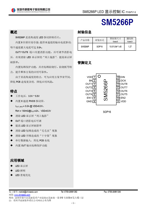
封装信息管脚定义GND EN1VDDEN2OUT5OUT6OUT7OUT8DCK DINSOP16特点◆ 工作电压:3.3V ~ 5.5V ◆ 内置8通道PMOS 驱动管,I OUT_MAX = 3.0A @ VDD=5.0V 、 Ron = 130mΩ@I OUT =2A 、VDD=5.0V ◆ 消除LED 显示屏“列上拖影” ◆ OUT 端口消影电压可调 ◆ 提高LED 显示屏刷新率◆ 消除LED 短路造成的“毛毛虫”现象 ◆ 消除LED 开路造成的“十字架”现象 ◆ 串行数据输入,简化PCB 布线 ◆ 内置OUT 输出短路保护功能应用领域◆ LED 显示屏 ◆ LED 照明 ◆ LED 景观亮化内部功能框图DINDCKBK……OUT8Fig. SM5266P内部功能框图管脚说明最大极限参数备注:表贴产品焊接最高峰值温度不能超过260℃,温度曲线依据J-STD-020 标准、参考工厂实际和锡膏商建议由工厂自行设定。
特性参数(若无特殊说明,VDD= 5.0V,Ta = 25℃)应用框图ROW0ROW1ROW2ROW3COL0COL2COL15……COL1ROW4ROW5ROW6ROW7 Fig. 8扫LED显示屏应用框图Fig. 16扫LED显示屏应用框图Fig. 32扫LED显示屏应用框图封装焊接制程明微电子所生产的半导体产品遵循欧洲RoHs标准,封装焊接制程锡炉温度符合J-STD-020标准。
BC-01 使用说明书

无线充电参数:输入功率:5V/2A 或9V/1.67A 输出功率:10W/7.5W/5W 无线充电距离3-6mm(max)转换效率:慢充≥70%,快充≥75%工作频率:110-205KHz蓝牙参数:蓝牙版本:5.0工作频率:2.4G 声道:立体声FM 频道:85-110MHz 蓝牙距离:≤10m TF 卡:最大支持32G包装清单:1*BC-011*汽车出风口夹子1*延长支架1*USB 数据线1*使用说明书产品参数产品名称:BC-01材料:防火 PC+ABS 颜色:黑色使用方法1.将夹子通过螺帽固定住本产品,确保支架可以灵活旋转2.接通电源:将产品通过电源线连接汽车内USB 充电口(快充模式需要使用高通快充适配器)3.按压出风口夹子固定至出风口,然后调整好位置并固定螺帽4.蓝牙使用:* BC01两边双灯闪烁为蓝牙模式,打开手机蓝牙,找到蓝牙设备BC01;进行连接配对* BC01显示屏闪烁为FM 调频模式,将频率调至与汽车收音机同一频率(FM 调频时,将汽车收音机 的频率调整到当地无电台频点,然后再将BC01的频率和汽车收音机频率调节一致) *配对成功,播放音乐*当放音乐时如果有杂音请上/下调整频率0.1MHZ 5.无线充电:*将带无线充电功能的手机放置在支架上与产品贴近即可充电(建议先将蓝牙设置好再放置手机进行充电)6.取出手机触摸开合按键会自动打开支架,然后取出手机特点1. Qi 认证无线充电标准2.快充支持10W/7.5W/5W,适用于安卓和苹果系统。
3. 无线支架感应:当手机摆放在无线蓝牙支架时,两边的夹臂会自动将手机夹住。
4. 异常感应:当支架上没有手机时,两边的夹臂会自动合拢。
5. 延伸支架可以灵活伸缩调节,可以很好的把手机调整到合适的位置,便于放置和取出。
6. 全新升级静音设计:使用静音马达,夹臂活动时没有马达噪音。
7. 360°旋转:支持360°角度旋转,便于找到最合适的位置对手机操作和放置取出8. 带有过流保护、过热保护、短路保护功能,使用更安全9. 认证:FCC/CE/ROHS保修服务本产品自购买之日起十二个月内在正常使用情况下无材料和工艺缺陷。
SMS0818 液晶显示模块使用说明书

◆SMS0818液晶显示模块的概述:SMS0818数码笔段型液晶显示模块(LCM),采用数码笔段型液晶显示器(LCD),可显示8位数字及66段提示符及1个小数点,低功耗,与MCU单片机采用三线式串口连接,广泛应用于智能电表。
◆SMS0818液晶显示模块的主要技术参数:显示容量: 8位数字+8组汉字+51段条状图+5段圆形标志+3段符号(”kW”“.h”和小数点)模块工作电压: 4.8~5.2V 模块最佳工作电压: 5.0V工作电流: 300μA(5.0V)字高: 12.5mm 7.5mm 环境相对湿度:<85%视角: 6:00 工作温度:-20~+60℃显示方式: 反射式正显示存储温度:-30~+70℃接口方式: 三线式串行接口(B型)◆SMS0818液晶显示模块的接口信号说明:1 VDD: 电源正极2 VSS电源地3 DI: 串行数据输入4 CLK:串行移位脉冲输入5 CS: 片选信号输入LCDBUF D7 D6 D5 D4 D3 D2 D1 D00 S8 S7 S6 S5 S1 S2 S3 S41 S16 S15 S14 S13 S9 S10 S11 S122 S24 S23 S22 S21 S17 S18 S19 S203 S32 S31 S30 S29 S25 S26 S27 S284 S40 S39 S38 S37 S33 S34 S35 S365 S48 S47 S46 S45 S41 S42 S43 S446 X X X X S49S51XS507 8D 8E 8F 8A 8C 8G 8B Z18 7D 7E 7F 7A 7C 7G 7B KW9 6D 6E 6F 6A 6C 6G 6B H6。
Riverdi 10.1 寸 TFT 显示屏数据手册说明书

ITEM CONTENTS UNIT LCD Type TFT/Transmissive/Normally Black/IPS / Size 10.1 Inch Viewing Direction Free / Outside Dimensions (W x H x D) 246.66 x 151.30 x 13.48 mm Active Area (W x H) 216.96 x 135.60 mm Pixel Pitch (W x H) 0.1695 x 0.1695 mm Resolution 1280 x 800 / Brightness 1000 cd/m 2 Color Depth 16.7 M / Pixel Arrangement RGB Vertical Stripe / Driver IC of Board STM32H747XIH6 / External SDRAM 64Mbit (32-bit access) / External Flash Memory 512Mbit / Supply Voltage for Module 6.0-36.0 V With/Without Touch Without Touch Panel / Weight 615 g STM32 EMBEDDED 10.1" DISPLAY DATASHEET RVT101HVSFWN00 Rev.1.1 2022-02-14 F T M O D U L E S P E C I F I C A T I O N Note 1: RoHS3 compliant Note 2: LCM weight tolerance: ± 5%.REVISION RECORDREV NO. REV DATE CONTENTS REMARKS1.0 2022-01-10 Initial release1.1 2022-02-14 Update the absolute maximum ratingof V to 0V-48.0VCONTENTSREVISION RECORD (2)CONTENTS (3)MODULE CLASSIFICATION INFORMATION (4)ASSEMBLY GUIDE (5)MODULE DRAWING (6)ABSOLUTE MAXIMUM RATINGS (7)ELECTRICAL CHARACTERISTICS (7)BACKLIGHT ELECTRICAL CHARACTERISTICS (7)ELECTRO-OPTICAL CHARACTERISTICS (8)BOARD INTERFACES AND CONNECTORS (10)USER INTERFACES (16)DISPLAY SEPCIFICATION (18)INSPECTION (18)RELIABILITY TEST (20)LEGAL INFORMATION (21)MODULE CLASSIFICATION INFORMATIONRV T 101 H V S F W N 00 1. 2. 3. 4. 5. 6. 7. 8. 9. 10.ASSEMBLY GUIDEMounting frameFor dimensions 3.5”, 4.3”, 5.0”, 7.0” and 10.1”, the product with mounting frame version is available. Thanks to the four catches attached to the side, frame provides strong assembly to the surface by mounting element (like the screw, see Figure 1). The frames are specially designed to fit Riverdi products perfectly. The diameter of the mounting hole is 3.5mm.Figure 1. Mounting frameABSOLUTE MAXIMUM RATINGSPARAMETER SYMBOL MIN MAX UNIT NOTESupply Voltage for Module VDD 0 48.0V Note 1Digital I/O signals Voltage - -0.5 3.3 Note 1, 2Operating Temperature T OP-20 70 °CStorage Temperature T ST-30 80 °CStorage Humidity (@ 25 ± 5°C) H ST10 - % RHOperating Ambient Humidity (@ 25 ± 5°C) H OP10 - % RHNote 1. Exceeding maximum values may cause improper operation or permanent damageto the unit.Note 2. Most of the GPIOs have the 5.0 V tolerant input voltage, please refer to the datasheetof STM32H747XIH6 for more details.ELECTRICAL CHARACTERISTICSPARAMETER SYMBOL MIN TYP MAX UNIT Supply Voltage for Module VDD_IN 6.0 12.0 36.0 VPOWER‘ENABLE’ = ‘0’***************************I VDD_IN=6.0 V-60 -uA ****************************I VDD_IN=12.0 V-147 -uA ****************************I VDD_IN=24.0 V-388 -uA ****************************I VDD_IN=36.0 V-629 -uAPOWER‘ENABLE’ = ‘1’***************************I VDD_IN=6.0 V - 851 - mA ****************************I VDD_IN=12.0 V- 412 - mA ****************************I VDD_IN=24.0 V- 226 - mA ****************************I VDD_IN=36.0 V- 160 - mAInput Voltage “H” Level V IH 2.0 - 3.3 V Input Voltage “L” Level V IL 0 - 0.8 V Note. POWER ‘ENABLE’ refers to pin 3, ‘ENABLE’ of the power input connector.By default, POWER ‘ENABLE’ = ‘1’,When POWER ‘ENABLE’ = ‘0’, the device is turned off.BACKLIGHT ELECTRICAL CHARACTERISTICSPARAMETER SYMBOL MIN TYP MAX UNIT NOTE Lifetime - - 50,000 - hours NOTE 1Note 1. Operating life means the period in which the LED brightness goes down to 50% ofthe initial brightness. Typical operating lifetime is the estimated parameter.ELECTRO-OPTICAL CHARACTERISTICSITEM SYMBOL CONDITION MIN TYP MAX UNIT RMK NOTEResponse Time Tr+Tfθ=0°∅=0° - 25 35 ms FIG 2. 4Contrast Ratio Cr 800 1000 - --- FIG 3. 1 Luminance δ- 75 - % FIG 3. 3 Figure 3.Contrast Ratio =Average Surface Luminance with all white pixels (P1,P2,P3,P4,P5) Average Surface Luminance with all black pixels (P1,P2,P3,P4,P5)Note 2.Surface luminance is the LCD surface from the surface with all pixels displaying white. For more information see Figure 3.Lv = Average Surface Luminance with all white pixels (P1, P2, P3, P4, P5)Note 3.The uniformity in surface luminance δWHITE is determined by measuring luminance at each test position 1 through 5, and then dividing the minimum luminance of 5 points luminance by maximum luminance of 5 points luminance. For more information see Figure 3.δ WHITE =Minimum Surface Luminance with all white pixels (P1,P2,P3,P4,P5) Maximum Surface Luminance with all white pixels (P1,P2,P3,P4,P5)Note 4. Response time is the time required for the display to transition from white to black (Rise Time, Tr) and from black to white (Decay Time, Tf). For additional information see Figure 2. The test equipment is Autronic-Melchers’s ConoScope series.Note 5. CIE (x, y) chromaticity, the x, y value is determined by measuring luminance at each test position 1 through 5, and then calculating the average value.Note 6. Viewing angle is the angle at which the contrast ratio is greater than 2. For TFT module the contrast ratio is greater than 10. The angles are determined for the horizontal or x axis and the vertical or y axis with respect to the z axis which is normal to LCD surface. For more information see Figure 4.Note 7. For viewing angle and response time testing, the testing data is based on Autronic-Melchers’s ConoScope series. Instruments for Contrast Ratio, Surface Luminance, Luminance Uniformity, CIE the test data is based on TOPCON’s BM-5 photo detector.Figure 2. The definition of response timeFigure 3. Measuring method for Contrast ratio, surface luminance, Luminance uniformity, CIE (x, y) chromaticityA: 5mmB: 5mmH, V: Active AreaLight spot size ∅=5mm, 500mm distancefrom the LCD surface to detector lens.Measurement instrument is TOPCON’Sluminance meter BM-5Figure 4. The definition of viewing angleBOARD INTERFACES AND CONNECTORSPower input connectorThe 1.25mm, 5-pin Molex connector labeled as “POWER’ is power input connector.There is an internal reverse polarity protection which ensures that the device is not damaged if the power supply polarity is reversed.NO. PIN DESCRIPTION NOTE1 VDD_IN Power supply input; 6.0-36.0VNote 12 VDD_IN Power supply input; 6.0-36.0V3 ENABLE Enable/ Disable power supply. Note 24 GND Ground5 GND GroundNote 1: STM32 Embedded Display allows to directly connect one additional display to the system. There is RiBUS connector on the board where you can connect any of intelligent display from Riverdi based on EVE4 (BT817Q). However, please note that it may change power supply requirement as below:The power supply voltage must range from 7.0V- 14.0 V (TYP. 9V), if Riverdi EVE4 10.1” series display is connected through RiBUS. At the same time, please also configure the backlight voltage jumpers, P5 and P12, according to subchapter 10.8, note 1.The power supply voltage ranges from 6.0 V- 36.0V if any of Riverdi EVE4 3.5”,4.3”,5.0” and 7.0” series display is connected through RiBUS. At the same time, please also configurethe backlight voltage jumpers, P5 and P12, according to subchapter 10.8, note 1.Note 2: By default, pin “ENABLE” is pull up to VDD and enabled. To disable, ground the pin to turn off the device completely.USB interfaceThe 1.25mm, 5-pin Molex connector labeled as “USB’ is USB interface.NO. PIN DESCRIPTION NOTE1 VCC_USB Power supply Note 12 D- USB data-3 D+ USB data+4 ID USB OTG ID; Host /Device detect Note 15 GND GroundNote 1. Configuration of the USB Host/Device mode:Host Mode: Pin 4 (ID) should be connected to GND.In this mode, it can provide +5V output voltage to the connected USB device and Max output current 500 mA.Device Mode: Pin 4 (ID) should be not connected (floating).RS485 interfaceThe 1.25mm, 4-pin Molex connector labeled as “RS485’ is RS485 interface.NO. PIN DESCRIPTION NOTE1 A Non-inverting receiver input and non-inverting driver output2 B Inverting receiver input and inverting driver output3 GND Ground4 VDD_IN Power supply input; 6.0-36.0VRS232 interfaceThe 1.25mm, 5-pin Molex connector labeled as “RS232’ is RS232 interface.NO. PIN DESCRIPTION NOTE1 RTS Request to send2 CTS Clear to send3 TXD Transmit Data4 RXD Receive Data5 GND Ground2 x CAN FD interfacesThe main board supports 2 channels of the CANFD (Control Area Network Flexible Data-Rate) communication bus, based on the high-speed (2.5-8.0Mbps) CAN transceiver.2 pcs of 1.25mm, 4-pin Molex connectors labeled as “CAN1’ and “CAN2” are r espectively interfaces of CAN FD1 and CAN FD2.NO. PIN DESCRIPTION NOTE1 GND Ground2 CAN_L CAN Low-Level Voltage3 CAN_H CAN High-Level Voltage4 VDD_IN Power supply input; 6.0 – 36.0 VHaptic feedback connectorThe 1.25mm, 2-pin Molex connector labeled as “HAPTIC’ is haptic feedback connector. Haptic feedback P7 is used to connect with the haptic motor directly.NO. PIN DESCRIPTION NOTE1 OUT+ Positive haptic driver differential outputNote 12 OUT_ Negative haptic driver differential outputNote 1: The haptic driver applies DRV2605L and is controlled by internal I2C1.SWD (Serial Wire Debug) connectorThe 1.25mm, 6-pin Molex connector labeled as “SWD” is SWD interface, which is used for programing the MCU on board.NO. PIN DESCRIPTION NOTE1 VCC_+3.3V Power input2 SW_CLK Serial wire clock3 GND Ground4 SW_DIO Serial wire debug data input/output5 RST Reset; Active low6 SWO Serial wire trace outputRiBUSAny size of the Riverdi EVE4 series display can be connected through RiBUS to act as a slave module to the mainboard.NO. PIN DESCRIPTION NOTE1 VCC_+3.3V Supply voltage for module; TYP3.3Vfrom 7.0 - 14.0V (TYP. 9V).For Riverdi EVE4 series display ranging from sizes of 3.5” to 7.0”,the backlight voltage (BLVDD) is 5V.Backlight jumper selectors, P5 and P12, labeled as “BLVDD SEL” are used to configure the backlight voltage range.Warning! When you configure the jumpers, be sure that the module is powered off.DO NOT change ANY jumpers while the module has power. Improper operation might cause permanent damage to the unit.Please also pay special attention to not misplace the jumpers. Incorrect jumpers setting may lead to damage to the module as well.Table 2. Backlight power (7.0V-14.0V) select jumpers settingExpansion connectorThe main board has one 1.27mm, 40-pin expansion pin header which is labeled as “EXPANSION CONNECTOR’,It provides direct access to below GPIOs of MCU STM32H747XIH6,which make it possible to easily extend a daughterboard for a specific application.• 2 x I2C• 1 x UART• 1 x USART• 1 x SPI• 1 x USB•7 x PWMs• 2 x DACs (Digital-to-analog)• 2 x ADCs (Analog-to-digital)Each of the GPIO pins can be configured by software as output (push-pull or open-drain, with or without pull-up or pull-down), as input (floating, with or without pull-up or pull-down) or as peripheral alternate function. Most of the GPIO pins are shared with digital or analog alternate functions. Please refer to the datasheet of MCU STM32H747XIH6 for more details.I/O PD13 15 16 PA3 I/OP GND 17 18 GND PI/O PC2 19 20 PA0_C I/OI/O PC3 21 22 PA1_C I/OI/O PA12 23 24 PC2_C I/OI/O PA9 25 26 PC3_C I/OI/O PA10 27 28 GND PI/O PJ8 29 30 PC13 I/OI/O P18 31 32 PA8 I/OI/O PJ10 33 34 PB11 I/OI/O PB0 35 36 PH4 I/OI/O PC6 37 38 PB12 I/OI/O PB14 39 40 PB15 I/ONote. The total output current I VCC=5V from pin 1 and pin3 is maximum 1A.The total output current I VCC=3.3V from pin 2 and pin 4 is maximum 500mA.Micro SD slotThe mainboard is equipped with Micro-SD slot, which supports all types of Micro SD cards.2 x 20-pin, 1.27 mm pin sockets for POE Add-on BoardThe 2 x 20-pin, 1.27 mm, pin sockets, labeled as U9a and U9b, are used to connect the Riverdi POE Add-on Board.The Riverdi POE Add-on Board features 10/100M Ethernet Port with Power-Over-Ethernet enabled. It allows you to power the module through the Ethernet port.Note: The Riverdi POE Add-on Board is sold separately.USER INTERFACES3 x push buttonsPush button labeled as “RST” is used to “RESET” the module.Another 2 push buttons labeled as BTN1, BTN2 are for user’s development.•BTN1(S1) is connected to pin 37, PC6, of the expansion connector.•BTN2(S2) is connected to pin 35, PB0, of the expansion connector.By default, R57 and R58 are not mounted. Please solder 0402 0R resistor or short R57, R58 to enable the pushbuttons BTN1(S1), BTN2(S2).3 x LEDs1 x LED, labeled as ‘PWR LED’, emits green light when the modules is powered.1 x LED, labeled as ‘USB OVR’, emits red light when VCC_USB pin is shorted.1 x LED, labeled as ‘USR LED’, is for user’s development.•The ‘USR LED’ is connected to pin 33, PJ10, of the expansion connector.By default, the resistor R60, (1k ohms) is soldered. Please remove R60 to use GPIO channel PJ10.D ISPLAY SEPCIFICATIONTFT resolutionThe supported resolution of the display in this module is 1280*800.Full TFT specificationFor detailed information on the display, please refer to datasheet of displayRVT101HVLFWN00.I NSPECTIONStandard acceptance/rejection criteria for TFT moduleInspection conditionAmbient conditions:•Temperature: 25 ± 2°C•Humidity: (60 ± 10) %RH•Illumination: Single fluorescent lamp non-directive (300 to 700 lux) Viewing distance: 35 ± 5cm between inspector bare eye and LCD.Viewing Angle: U/D: 45°/45°, L/R: 45°/45°Inspection standardThe LCD TFT has zero bad pixels. Please refer the item “Bright/Dark dots”. ITEM CRITERIONBlack spots,white spots,light leakage,Foreign Particle(round Type)D=(x+y)/2Spots density: 10 mmSize =10.1”Average Diameter Qualified QtyD ≤ 0.2 mm Ignored0.2 mm < D ≤ 0.3 mm N≤40.5mm < D N = 0LCD black spots,white spots,light leakage(line Type)Spots density: 10 mmSize =10.1”Length WidthQualifiedQty - W ≤ 0.05Ignored L ≤ 5.00.05< W ≤ 0.1N ≤ 3 5.0 < L0.10< W5.0 < LN = 0Bright/Dark DotsSize =10.1”Item Qualified Qty Bright dots 0Dark dots 0 Cluster Bright Dots or Dark Dots 0 Total Bright and Dark Dots 0Clear spotsSize ≥ 5”Average Diameter Qualified QtyD < 0.2 mm Ignored0.2 mm < D < 0.3 mm 40.3 mm < D < 0.5 mm 20.5 mm < D 0 Spots density: 10 mmTouch panel spotSize ≥ 5"Average Diameter Qualified QtyD < 0.25 mm Ignored0.25 mm < D < 0.5 mm 40.5 mm < D 0Touch panel White line ScratchSize ≥ 5"Length Width Qualified Qty - W < 0.03 IgnoredL < 5.0 0.03 < W < 0.05 2- 0.05 < W 0RELIABILITY TESTNO.TEST ITEMTEST CONDITIONNOTE1 High Temperature Storage 80°C/120 hoursNote 12 Low Temperature Storage -30°C/120 hours3 High Temperature Operating 70 °C /120 hours Note 2. Before cosmetic and function test, the product must have enough recovery time, at least 2 hours at room temperature.© 2022 Riverdi Page 21 of 21 RVT101HVSFWN00L EGAL INFORMATIONRiverdi grants the guarantee for the proper operation of the goods for a period of 12 months from the date of possession of the goods. If in a consequence of this guaranteed execution the customer has received the defects-free item as replacement for the defective item, the effectiveness period of this guarantee shall start anew from the moment the customer receives the defects-free item.Information about device is the property of Riverdi and may be the subject of patents pending or granted. It is not allowed to copy or disclosed this document without prior written permission.Riverdi endeavors to ensure that all contained information in this document is correct but does not accept liability for any error or omission. Riverdi products are in developing process and published information may be not up to date. Riverdi reserves the right to update and makes changes to Specifications or written material without prior notice at any time. It is important to check the current position with Riverdi.Images and graphics used in this document are only for illustrative the purpose. All images and graphics are possible to be displayed on the range products of Riverdi, however the quality may vary. Riverdi is no liable to the buyer or to any third party for any indirect, incidental, special, consequential, punitive, or exemplary damages (including without limitation lost profits, lost savings, or loss of business opportunity) relating to any product, service provided or to be provided by Riverdi, or the use or inability to use the same, even if Riverdi has been advised of the possibility of such damages.Riverdi products are not fault tolerant nor designed, manufactured or intended for use or resale as on line control equipment in hazardous environments requiring fail –safe performance, such as in the operation of nuclear facilities, aircraft navigation or communication systems, air traffic control, direct life support machines or weapons systems in which the failure of the product could lead directly to death, personal injury or severe physical or environmental damage (‘High -Risk Activities’). Riverdi and i ts suppliers specifically disclaim any expressed or implied warranty of fitness for High-Risk Activities. Using Riverdi products and devices in 'High-Risk Activities' and in any other application is entirely at the buyer’s risk, and the buyer agrees to def end, indemnify, and hold harmless Riverdi from all damages, claims or expenses resulting from such use. No licenses are conveyed, implicitly or otherwise, under any Riverdi intellectual property rights.。
诺瓦科技LED显示屏HDMI接收卡SX100规格书

SX100
HDMI 接收卡
司 公 限 有 技 科 子 电 瓦 诺 SX100 是诺瓦科技开发的一款兼备发送和接收功能的二合一 HDMI 控制卡,极大地简化了 LED 显示系 安 统的连接,让用户体验更加方便。 西 单卡可带载 512×384 像素点,支持一路 HDMI 视频源输入和一路 HDMI 视频源输出级联的功能,支
25
26
GND
接地
/
B16
27
28
G16
/
/
R16
29
30
B15
/
/
G15
31
32
R15
/
/
B14
33
34
G14
/
/
R14
35
36
B13
/
/
G13
37
38
R13
/
/
B12
39
40
G12
//R1241源自42B11/
第3页
/
G11
43
44
R11
/
/
B10
45
46
G10
© 2017 西安诺瓦电子科技有限公司 版权所有 本资料中技术参数如有改动,恕不另行通知
第9页
74HC164 时钟输入 H164_CLK
65
接地
GND
67
66 68
H164_CSD LCD_BL0
司 74HC164 数据输入
LCD 的背光信号 1
LCD 的背光信号 2
LCD_BL1
69
70
LCD_SCL
WFT09(S)II 简易说明书 CN

1024/4096PCMS九通道2.4GHz遥控器感谢选用天地飞产品。
请在使用前详细阅读使用说明书,确保使用安全。
●售后服务●安全提示●产品配置如果您忽略此标志所指的操作说明,而做出错误的操作,有可能会造成使用者或他人死亡等严重危险伤害。
如果您忽略此标志所指的操作说明,而做出错误的操作,有可能会造成使用者或他人严重伤害或物品损坏。
如果您忽略此标志所指的操作说明,而做出错误的操作,有可能会造成使用者或他人的伤害或者物品损坏。
任何情况下都禁止尝试的操作。
任何情况下都请您务必遵守。
标志含义危险警告注意禁止务必遵守1.本使用说明书所记载的产品,在国内的无线电法令规定下,用途仅限于模型应用。
2.本产品在改装、调整、更换零件后,本公司将不负任何责任,敬请谅解。
本产品的用途、改装等注意事项1.WFLY 产品自购买之日起,属于质量问题一年内由深圳市天地飞科技开发有限公司免费保修(公司承担往返邮费)。
2.WFLY 产品自购买之日起七天内,在正常使用的情况下出现质量问题,外观无损坏,可凭保修卡及购机凭证在经销商处免费更换同型号产品;经销商收到更换产品时必须第一时间通知公司予以备案更换。
3.WFLY 产品将由深圳市天地飞科技开发有限公司提供终身售后服务;对于自购买之日起,人为损坏、改装、开盖损坏封条以及超过一年免费保修期的,用户必须支付往返邮费、材料成本费及维修成本费用。
4.为确保您的权益受到保护,并能及时有效的为您服务。
请在购买WFLY 产品时务必完整填写好保修卡及索要购机凭证;由销售商签字盖章。
用户享受本售后服务条款必须提供保修卡及购机凭证,缺一不可;销售商没有给消费者保修卡或不按要求填写的,由销售商承担全部的售后服务费用。
5.本售后服务条款仅限于中国大陆销售的WFLY 产品。
售后服务注意警告安全提示 (注意事项)在使用前请确认商品的配件是否都有备齐,接收机是否已经正常连接三线开关,舵机,遥控器与接收机是否都连接好了电源,以及确认是否都可开启并且有正确的动作后再使用。
CH19264B液晶模块中文使用说明书
-
+5.5
0
-
7.0
-0.3
-
VDD+0.3
单位
V V V
Page 6
ch
深圳市川航电子科技有限公司 ShenZhen ChuanHang Electronic Technology CO.,LTD
TEL: 0755-29035962 E-mail: chuanhanglcm@
Page 3
ch
深圳市川航电子科技有限公司 ShenZhen ChuanHang Electronic Technology CO.,LTD
TEL: 0755-29035962 E-mail: chuanhanglcm@
1.概述
CH19264B点阵绘图型液晶显示模块(LCM),采用192x64点阵液晶显示屏(LCD) 与低功耗LED背光组成。由2个ST7920控制,每屏可显示12x4排汉字,内置8192个 16x16点的中文字型以及126个16x8点半宽的字母符号型,另外提供一个64x256 点的绘图区域(GDRAM)及240点的ICON RAM,可以和文字画面混和显示,而且 ST7920內含CGRAM。提供8位,4位和串口三种微处理器接口,可与MCU单片机直接 连接,广泛应用于各类仪器仪表与电子设备上。
SM16159 LED显示驱动芯片说明书
SM16159概述SM16159是LED 高密全彩屏专用驱动芯片,内置16K 的SRAM 存储结构,能够存储一帧完整显示数据,支持1~32扫LED 显示屏整帧数据存储及显示。
此方式降低了数据时钟频率,并可实现高灰阶效果。
SM16159内建16位灰阶控制的脉冲宽度调变功能,16个恒流输出通道所输出的电流值不受输出端负载电压的影响并提供一致且恒定的输出电流。
可通过选用外接电阻或调节6位电流增益来调整整体LED 的驱动电流。
封装信息特点◆ 内置64级电流增益调节功能 ◆ 内置16k SRAM ,支持1~32扫 ◆ 行扫倍频技术,刷新率提升2/4/8倍◆ 内置开路检测功能,解决开路“十字架”问题 ◆ 内置列下消影功能◆ 内置偏色、低灰麻点、第一扫偏暗改善功能 ◆ 16位PWM 灰阶控制可调显示刷新率SM_PWM专利技术◆ 工作电压:3.3V~5.0V◆ 输出恒流范围:0.6~32mA@VDD=5.0V ;0.6~24mA@VDD=3.3V ◆ 输出电流精度:通道间偏差:<±2.0%(最大值) 芯片间偏差:<±2.5%(最大值)管脚定义111213141516171819202122231098765432124OUT4OUT3OUT5OUT6OUT7OUT2OUT1OUT0LE DCLK SDI GND OUT8OUT9OUT10OUT11OUT12OUT13OUT14OUT15GCLK SDO REXT VDDS D ID DE X TD OC L KO U T OUT3OUT2OUT1OUT0LE OUT4C L KO U T G N DO U T O U T O U T内部功能框图LESDISDO管脚说明订购信息输出及输入等效电路GCLK,DCLK,SDI输入端LE输入端SDO输出端最大限定范围静态特性(V静态特性(V动态特性(V动态特性(V*在时序波形图(1)中,LE下降延后SDO的输出变化。
上海仪电科学仪器股份有限公司产品说明书
敬告用户:●请在使用本仪器前,详细阅读本说明书。
●仪器超过一年必须送计量部门或有资格的单位复检,合格后方可使用。
●用户在实际的使用中需要接触如浓硫酸等有害的化学物质,以及其他强氧化剂、强腐蚀性的物质,如铬酸洗液等,因此用户在操作时务必要小心谨慎,注意不要溅在身体或衣物上,以免灼伤身体或损坏仪器,对您造成不必要的损失。
●对于具有强腐蚀性的洗液还要注意回收,用户用毕要回收废液,可反复使用。
分析结束后应集中收集,妥善处理。
●比色管是易碎品,用户应尽量轻拿轻放,避免使用很大的力量插入比色池中,反之亦然。
为了更好地固定比色管,比色池设计的固定装置可能比较紧,用户拿放比色管时请注意。
●如果仪器右上角显示“电池”标志时,表示电池电量不足,建议用户尽快更换电池,以免电池电量耗尽仪器停止工作而影响测量。
●在更换电池前请先关机,然后再更换电池。
●比色管为易耗品,用户可与本厂联系购买!目录1 安装 (3)1.1开箱 (3)1.2仪器结构 (3)1.3仪器安装 (4)2 操作指南 (4)2.1 简介 (4)2.2 仪器主要技术性能 (5)2.3 键盘说明 (5)2.4 仪器操作 (9)2.4.1 仪器的开/关机 (9)2.4.2 仪器的起始状态 (9)2.4.3 数据查阅功能 (9)2.4.4 测量 (9)2.4.4.1 常规测量步骤 (9)2.4.4.2 测量前的准备 (10)2.4.4.3 标定 (11)2.4.4.4 余氯的测量 (13)2.4.4.5 总氯的测量 (14)2.4.4.6 测量结束后处理 (14)3 仪器的维护 (15)3.1 仪器的维护 (15)3.2 常见故障排除 (15)4 附件信息 (15)5 附录 (16)附录1 余氯、总氯测定所需试剂的配制 (16)附录2 比色管筛选和标记参考 (18)附录3 故障现象与故障排除表 (19)1安装1.1 开箱在便携式余氯/总氯包装箱中可找到以下部件:1.DGB-402A型便携式余氯/总氯测定仪l台2.比色管5只3.附件1套1.2 仪器结构1.2.1 仪器正面图1.2.2 仪器背面图1.2.3 仪器附件接下来将为您介绍仪器的几种重要的配件、选配件及附件,他们是保证您实现仪器某种功能所不可缺少的。
SG320240-01B 系列说明书
SG320240-01B系列说明书(Version1.0)可选型号:产品型号及其后缀LCD类型(显示模式)背光类型时序方式逻辑电压(VDD)背光电压接口方式及其预留配置SG320240SBD-01BCWE STN 蓝底色CCFL 无控制器 3.3~5.0V需配CCFL逆变器单排插针焊位FFC插座焊位SG320240SBD-01BCWE(DN) STN 蓝底色CCFL 无控制器 3.3~5.0V需配CCFL逆变器单排插针焊位FFC插座焊位SG320240SBD-01BCWE(CN) STN 蓝底色CCFL 68、80时序 3.3~5.0V需配CCFL逆变器双排插针焊位FFC插座焊位SG320240SBD-01BCWE(CD) STN 蓝底色CCFL 68、80时序 3.3~5.0V需配CCFL逆变器双排插针焊位FFC插座焊位标准配置:LCM无后缀表示为标准配置,标准配置的LCM不带控制器,不带负电源,80时序。
可扩展功能:1.DN:模块不带控制器,带负电源输出。
:模块带SED1335或替代IC RA8835控制器,但不带负电源输出。
3.CD:模块带SED1335或替代IC RA8835控制器,并且带负电源输出。
4.上述LCM可以选择68时序使用。
5.上述LCM可以选择3.3V逻辑电压使用。
但需要单独声明、特殊配置。
注:以上列出LCD类型只有STN 蓝底色,背光尚有白色LED可选,组合方式及扩展功能如上表,如果有其他需求,请致电我公司销售部。
销售部:电话:010-******** 136********QQ:1056456564文档修订记录修订修订次第修订 日期修订人修订前版本号页次章节 编号修订内容简述 批准人1 2007-1-23 王梅 / / /新建文档趙鵬目录1、液晶显示模块整体描述 (4)2. 最大典型值 (5)3. 电气特性 (5)4. LCD驱动电源连接方式 (5)5. 接口引脚定义 (7)6. 外形尺寸图纸 (10)7.液晶显示模块在使用过程中的注意事项 (11)8.测试程序 (13)1、液晶显示模块整体描述项目说明单位液晶显示模块组成液晶显示屏,背光灯箱,线路板,铁框液晶显示屏类型正像反射型,半透型,负像型液晶屏显示类型 STN型:蓝模式FSTN型O’clock液晶显示屏视角 6液晶模块外形尺寸 (LED*) 139.00(长)×120.00(宽)×13.20(厚) mm液晶模块视域 103.00(长)×79.00(宽) mm 液晶模块铁框尺寸 (LED*) 122.20(长)×100.00(宽)×13.20(厚) mm液晶显示模块点阵数 320×240点阵mm 液晶显示屏点尺寸 0.27(长)×0.27(宽)mm 液晶显示屏点间距 0.30(长)×0.30(宽) 液晶显示屏占空比 1/240液晶显示屏偏置电压 1/17液晶显示模块控制器 SED1335、RA8835A 或不带控制器方式液晶显示模块使用温度范围(E*) -20~+70 ℃液晶显示模块存储温度范围(E*) -30~+80 ℃背光灯箱 LED白背光或CCFL 液晶显示模块数据输入格式八位并行输入格式, 68、80时序方式电源输入电压 3.3~5V输入供电,内置DC/DC电路V液晶显示模块理论寿命 50,000 小时注意: LED*: LED背光E*: 宽温等级2. 最大典型值2.1 电气最大典型值 Vss=0VItem Symbol Min Max Unit Note 逻辑电源 Vdd -Vss 0 6.0 V LCD 驱动电压 Vdd -V o 0 24.0 V I/O 口输入电压 Vi 0 Vdd V2.2 使用环境最大典型值ItemSymbol Min Max Unit 工作温度 T0 -20 +70 ℃ 储存温度 Ts -30 +80 ℃ 湿度------85%RH3. 电气特性3.1 电气特性Vss=0VItem SymbolCondition Min TypMax Unit逻辑电压 Vdd ---- 2.7 5.0 5. 5 V LCD 驱动电压 Vdd -Vo ---- 15.5 --- 19.8 V 输入电压最大值 VIH ---- Vdd-2.2--- Vdd V 输入电压最小值 VIL---- 0 --- 0.8 V 频率 FELMVdd=5V 65 7885 Hz3.2 LED 背光特性Color Item Symbol Min Typ Max Unit Condition白色侧背光 正向电压 Vf 2.8 3.0 3.2 V If =140mA4. LCD驱动电源连接方式模块带负电压电路的使用下图方法(电位器可以选10K-20K)模块不带负电压电路的使用下面的方法(电位器可以选10K-20K)5. 接口引脚定义CN1、FFC2:不带控制器的模块使用,其中CN1为单排焊盘插针使用,FFC2为FFC方式使用。
- 1、下载文档前请自行甄别文档内容的完整性,平台不提供额外的编辑、内容补充、找答案等附加服务。
- 2、"仅部分预览"的文档,不可在线预览部分如存在完整性等问题,可反馈申请退款(可完整预览的文档不适用该条件!)。
- 3、如文档侵犯您的权益,请联系客服反馈,我们会尽快为您处理(人工客服工作时间:9:00-18:30)。
北京融视科技发展有限公司 P10单红异步控制版
LED
显示屏使用说明书
前言
感谢您选择北京融视科技发展有限公司LED显示屏产品,本说明书适用于P10单元板异步U盘控制显示屏。
北京融视LED显示屏控制软件无需安装,直接拷贝在任意目录即可。
运行软件
打开LED显示屏控制软件文件夹,看到如下文件:
单击LedNewWindow.exe 文件,进入运行界面。
注:对于U盘控制卡来说软件运行时会弹出
对话框,这是由于软件没有发现串口连接造成的,点击确定即出现软件运行界面
显示屏的硬件设置
注:融视光电在给客户发送软件时已经进行了硬件设置,如果您无需改动可跳过此步。
·点击菜单栏按钮,出现密码输入窗口:
初始默认管理员登录密码为168。
输入正确密码,即进入硬件配置窗口:
对于P10单红系列产品显示屏来说您只需设置即可。
注:显示屏尺寸不同,高度、宽度的设置参数也不一样,您的显示屏尺寸参数在给您提供软件之前已经设置完毕,请您妥善保管。
如果遗失,您只需提供给我们您的显示屏尺寸,我们即可给提供正确的显示屏高度、宽度参数。
设置完显示屏高度、宽度参数后,点击后,再点击关闭即可。
输入一行走字文字
新建节目
·点击文件菜单,选择新建,在软件左侧的“节目管理”窗口中即出现新建的节目信息。
·在“节目管理”窗口中选择,开始对节目以进行设置。
·点击节目管理中的“分区”按钮,并选择单行文本。
现在您就有了一个可以输入文本的条目。
3.2输入一行LED显示屏上要显示的文本
·选择,在属性编辑窗体中输入“北京融视科技发展有限公司”:
·设置文字的高度,本例为
·设置分区的尺寸
在软件界面的右下角的“分区属性”窗口中设置分区尺寸,分区尺寸不能超过上面硬件设置中的显示屏尺寸。
本例为高度32,宽度288。
好,现在一个可显示的走字文本已经录入成功。
·将您的节目保存到U盘。
注:您必须使用纯粹的U盘,而不是mp3、录音笔等有存储功能的电子产品代替,否则控制卡无法分别哪个文件保存的是节目信息。
单击,在“U盘数据保存对话框”中选择您的U盘路径,并单击保存即可。
在LED显示屏上显示录入的文字
显示屏接通电源,将U盘直接插入到显示屏的U盘接口,直到显示屏上显示“录入完毕”,拔下U盘即可看到刚录入的文字。
附录
附录1:使用注意事项:
1:严禁半户外显示屏安装于户外淋雨或可浸水处;
2:显示屏安装必须离地至少5cm空间;
3:严谨带电对显示屏内部零部件进行插拔;
4:室外显示屏安装需用角铁或角铝,严禁使用过薄安装件,避免显示屏跌落。
5:严禁使用长度超过显示屏型材边框厚度的螺丝或其他安装件在显示屏上打孔,以免钻穿电路板;
6:全户外显示屏上边框、背板、固定自钻螺丝全部使用LED专用密封胶做防水处理,请勿刮去表面密封胶;
7:由于单片机控制芯片的局限,控制卡软件暂时不支持Vista、windows7操作系统。
附录2:LED显示屏常见问题
1:显示屏有一半花屏或者两头同时走字
软件中显示屏的尺寸设置不正确,从新在软件的“硬件设置”选项卡中进行硬件设置。
2:显示屏的时间显示不正确
U盘控制卡在保存到u盘对话框中选择“本次操作包含u盘时间校对”,更新显示屏时间。
3:显示屏不读取u盘或者显示加载失败
·在软件编辑完毕后是否已经将数据点击软件的“保存到u盘”将编辑的数据录入
到u盘中;
·u盘是否正常,请不要用mp3、录音笔之类u口设备进行显示屏录入;
·usb线线路问题,进行usb线路检查。
4:显示屏部分不亮或整屏不亮
·进行电路检查,查看是否已经开机;
·查看软件自动开关机设置(仅限网口控制和串口控制),是否已经设置成关机状态;
·查看显示屏中是否包含可播放节目节目;
·显示屏电源故障。
整屏不亮为控制卡侧电源损坏,部分不亮为不亮部分电源损坏;5:显示屏花屏
·检查软件中显示屏的尺寸设置是否正常;
·检查是否软件存在病毒等问题,从新更换软件;。