LTC电源管理芯片
电源管理芯片型号
电源管理芯片型号电源管理芯片是一种用于控制和管理电源供应的集成电路,常用于电子设备和计算机系统中。
它能够监测电源电压、电流和温度等参数,以确保电子设备或计算机系统正常工作,并保护设备免受过电压、过电流和过温等不良条件的损害。
电源管理芯片的型号有很多种,下面简单介绍几种常见的型号。
1. MAX77650:这是一款高性能、集成度很高的电源管理芯片。
它具有多种功能,包括锂电池充放电管理、电源管理和系统监测等。
它采用低功耗设计,能够延长电池寿命,同时提供多种省电模式。
2. TPS54160:这是一款高效率、同步降压型电源管理芯片。
它适用于工业和通讯设备,能够提供稳定的电源输出。
它的主要特点是高效率和低纹波,能够满足电子设备对稳定电源的要求。
3. LT3652:这是一款微型化、高效率的电源管理芯片。
它适用于锂电池充电和电源管理。
它采用了开关电源技术,能够提供高效率的电源转换,同时集成了多种保护机制,能够确保电子设备的安全使用。
4. LTC6804:这是一款用于电池管理的芯片。
它可以对电池进行均衡充放电,并能够监测电池的电压、温度和容量等参数。
它采用高精度的ADC技术,能够提供准确的电池状态监测。
5. BQ25895:这是一款专用于充电管理的芯片。
它支持快速充电和逆变充电模式,能够根据不同设备的需求,选择合适的充电模式。
同时,它还具有多种保护机制,能够保护设备免受过充、过放和短路等不良条件的损害。
以上仅是部分电源管理芯片的型号介绍,每一款型号都有自己的特点和应用场合。
随着电子设备的不断发展,电源管理芯片的功能和性能也在不断提高,以满足电子设备对高效、稳定和安全电源供应的需求。
LTC4054丝印LTH7锂电充电管理IC
LTC4054丝印LTH7锂电充电管理IC————————————————————————————————作者:————————————————————————————————日期:2V1.31)典型应用电路注:R1 电阻建议不要省列与 C 1 构成 R C 滤波防止过充电压。
如果 R 1 电阻不接 C 1 使用 10UF 以上电容。
典型运用电路仅供参考,其它以实际运用为准。
概述HX4054A 是一款单节锂离子电池恒流/恒压线性充电器,简单的外部应用电路非常适合便携式设备应用,适合 USB 电源和适配器电源工作,内部采用防倒充电路,不需要外部隔离二极管。
热反馈可对充电电流进行自动调节,以便在大功率操作或高环境温度条件下对芯片温度加以限制。
HX4054A 充电截止电压为 4.2V, 充电电流可通过外部电阻 进行设置。
当充电电流降至设定值的 1/10 时,HX4054A 将自动结束充电过程。
当输入电压被移掉后,HX4054A 自动进入低电流待机状态,将待机电流降至 1uA 以下。
HX4054A 在有输入电源时也可置于停机模式,从而将工作电流降至 30uA 。
兼容TP4054 XT4054 LN2054 SE9016 ME4054 XT4052 EUP8054 AS3020 XZ3085A BL8572 HX6001 QX4054 HYM4054 SUN4054 FK5406 AP5056 SLM4054 LP4054 APL3202 OPC8020 OHL5100 LM2054 UCT3054 TQ7051 特点∙ 锂电池正负极反接保护(没充电的情况下 ∙ 最大充电电流:500mA∙ 无需 MOSFET 、检测电阻器和隔离二极管 ∙ 智能热调节功能可实现充电速率最大化 ∙ 智能再充电功能 ∙ 预充电压:4.2V±1% ∙ 3C/10 充电终止 ∙ 待机电流 30uA∙ BAT 超低自耗电 1uA ∙ 2.9V 涓流充电阈值∙ 单独的充电、结束指示灯控制信号 ∙封装形式:SOT23-5应用∙ 手机、PDA 、MP3/MP4 ∙ 蓝牙耳机、GPS ∙ 充电座∙数码相机、Mini 音响等便携式设备V1.32管脚定购信息SOT23-5L封装 定购型号 包装形式产品正印SOT23-5LHX4054A极限参数(注 1)符号 参数额定值 单位 VCC 输入电源电压 -0.3~7 V PROG PROG 脚电压 -0.3~0.3 V BAT BAT 脚电压 -0.3~7 V CHRG CHRG 脚电压-0.3~7 V T BAT_SHTBAT 脚短路持续时间 连续 - I BAT BAT 脚电流 600 mA I PROG PROG 脚电流 600 uA T OP 工作环境温度 -40~85 ℃ T STG储存温度 -65~125 ℃ ESDHBM2000 V MM200V注 1:最大极限值是指超出该工作范围芯片可能会损坏。
ltc4413原理
ltc4413原理LTC4413是一款用于电源管理的芯片,其原理基于电源选择和电源切换功能。
本文将对LTC4413的工作原理进行详细介绍。
LTC4413芯片是一种电源选择器,用于选择两个不同的电源之间的优先级。
它可以自动监测电源的电压和电流,并根据预设的优先级选择最佳的电源。
这款芯片主要用于电池备份系统、电池充电系统以及其他需要实现电源切换和管理的应用。
LTC4413芯片具有多种保护功能,如过压保护、欠压保护和过流保护等。
当其中一个电源的电压超过或低于预设阈值时,芯片会自动切换到另一个电源,以保护电路和设备的安全运行。
LTC4413芯片的工作原理如下:首先,根据预设的优先级,芯片会自动选择其中一个电源作为主要电源。
然后,它会监测主要电源的电压和电流,以及备用电源的电压。
如果主要电源的电压正常,则芯片会将其输出到负载上。
如果主要电源的电压异常(如过高或过低),芯片会自动切换到备用电源,并将其输出到负载上。
LTC4413芯片还具有电源切换的功能。
当主要电源失效或被拔掉时,芯片会自动切换到备用电源。
这种切换过程是无缝的,可以确保负载的电源持续供应。
当主要电源恢复正常时,芯片会再次自动切换回主要电源,以保持系统的稳定运行。
除了电源选择和切换功能外,LTC4413芯片还具有多种保护功能。
例如,当主要电源的电压超过设定值时,芯片会自动切断电源,以防止电路和设备的损坏。
当备用电源的电流超过设定值时,芯片也会自动切断电源,以保护电路和设备的安全运行。
LTC4413是一款功能强大的电源管理芯片,它可以实现电源选择、切换和保护等多种功能。
通过自动监测电源的电压和电流,并根据预设的优先级选择最佳的电源,该芯片可以确保负载的电源持续供应,同时保护电路和设备的安全运行。
在电池备份系统、电池充电系统以及其他需要实现电源切换和管理的应用中,LTC4413芯片具有广泛的应用前景。
锂电池管理芯片LTC1960

1234SYMBOL PARAMETER CONDITIONS MIN TYP MAX UNITS t ONPI Gate B1I/B2I/DCI Turn-On Time V GS < –3V, C LOAD = 3nF (Note 5)300µs t OFFPI Gate B1I/B2I/DCI Turn-Off Time V GS > –1V, C LOAD = 3nF (Note 5)10µs V PONI Input Gate Clamp Voltage I LOAD = 1µAGB1I Highest (V BAT1 or V SCP) – V GB1I 4.75 6.77.5VGB2I Highest (V BAT2 or V SCP) – V GB2I 4.75 6.77.5VGDCI Highest (V DCIN or V SCP) – V GDCI 4.75 6.77.5V V POFFI Input Gate Off Voltage I LOAD = –25µAGB1I Highest (V BAT1 or V SCP) – V GB1I0.180.25VGB2I Highest (V BAT2 or V SCP) – V GB2I0.180.25VGDCI Highest (V DCIN or V SCP) – V GDCI0.180.25V Logic I/OI IH/I IL SSB/SCK/MOSI Input High/Low Current●–11µA V IL SSB/MOSI/SCK Input Low Voltage●0.8V V IH SSB/MOSI/SCK Input High Voltage●2V V OL MISO Output Low Voltage I OL = 1.3mA●0.4V I OFF MISO Output Off-State Leakage Current V MISO = 5V●2µA SPI Timing (See Timing Diagram)T WD Watch Dog Timer● 1.2 2.5 4.5sec t SSH SSB High Time680ns t CYC SCK Period C LOAD = 200pF R PULLUP = 4.7k on MISO●2µs t SH SCK High Time680ns t SL SCK Low Time680ns t LD Enable Lead Time200ns t LG Enable Lag Time200ns t su Input Data Set-Up Time●100ns t H Input Data Hold Time●100ns t A Access Time (From Hi-Z to Data Active on MISO)●125ns t dis Disable Time (Hold Time to Hi-Z State on MISO)●125ns t V Output Data Valid C L = 200pF, R PULLUP = 4.7k on MISO●580ns t HO Output Data Hold●0ns t Ir SCK/MOSI/SSB Rise Time0.8V to 2V250ns t If SCK/MOSI/SSB Fall Time2V to 0.8V250ns t Of MISO Fall Time2V to 0.4V, C L = 200 pF●400nsNote 1: Stresses beyond those listed under Absolute Maximum Ratings may cause permanent damage to the device. Exposure to any Absolute Maximum Rating condition for extended periods may affect device reliability and lifetime.Note 2. Battery voltage must be adequate to drive gates of PowerPath P-channel FET switches. This does not affect charging voltage of the battery, which can be zero volts.Note 3. See Test Circuit.Note 4. DCIN, BAT1, BAT2 are held at 12V and GDCI, GB1I, GB2I are forced to 10.5V. SCP is set at 12.0V to measure source current at GDCI,GB1I and GB2I. SCP is set at 11.9V to measure sink current at GDCI, GB1I and GB2I.Note 5. Extrapolated from testing with C L = 50pF.Note 6. VDAC offset is equal to the reference voltage, sinceV OUT = V REF(16mV • VDAC(VALUE)/2047 + 1).Note 7. The LTC1960C is guaranteed to meet specified performance from 0°C to 70°C and is designed, characterized and expected to meet specified performance at –40°C and 85°C, but is not tested at these extended temperature limits.ELECTRICAL CHARACTERISTICS The ●denotes specifications which apply over the full operating temperature range (Note 7), otherwise specifications are at T A = 25°C. V DCIN = 20V, V BAT1 = 12V, V BAT2 = 12V unless otherwise noted.51960fa6781960faInput Power RelatedSCN (Pin 4/Pin 30): PowerPath Current Sensing Negative Input. This pin should be connected directly to the “bot-tom” (output side) of the low valued resistor in series with the three PowerPath switch pairs, for detecting short-circuit current events. Also powers LTC1960 internal circuitry when all other sources are absent.SCP (Pin 5/Pin 31): PowerPath Current Sensing Positive Input. This pin should be connected directly to the “top”(switch side) of the low valued resistor in series with the three PowerPath switch pairs, for detecting short-circuit current events.GDCO (Pin 6/Pin 32): DCIN Output Switch Gate Drive.Together with GD CI, this pin drives the gate of the P-channel switch in series with the DCIN input switch.GDCI (Pin 7/Pin 33): D CIN Input Switch Gate D rive.Together with GDCO, this pin drives the gate of the P-channel switch connected to the DCIN input.GB1O (Pin 8/Pin 34): BAT1 Output Switch Gate Drive.Together with GB1I, this pin drives the gate of the P-channel switch in series with the BAT1 input switch.GB1I (Pin 9/Pin 35): BAT1 Input Switch Gate D rive.Together with GB1O, this pin drives the gate of the P-channel switch connected to the BAT1 input.GB2O (Pin 10/Pin 36): BAT2 Output Switch Gate Drive.Together with GB2I, this pin drives the gate of the P-channel switch in series with the BAT2 input switch.GB2I (Pin 11/Pin 37): BAT2 Input Switch Gate D rive.Together with GB2O, this pin drives the gate of the P-channel switch connected to the BAT2 input.CLP (Pin 24/Pin 13): This is the Positive Input to the Supply Current Limiting Amplifier CL1. The threshold is set at 100mV above the voltage at the DCIN pin. When used to limit supply current, a filter is needed to filter out the switching noise.Battery Charging RelatedV SET (Pin 13/Pin 1): The Tap Point of a Programmable Resistor Divider which Provides Battery Voltage Feedback to the Charger. A capacitor from CSN to V SET and one from V SET to GND provide necessary compensation and filter-ing for the voltage loop.I TH (Pin 14/Pin 2): This is the Control Signal of the Inner Loop of the Current Mode PWM. Higher I TH corresponds to higher charging current in normal operation. A capaci-tor of at least 0.1µF to GND filters out PWM ripple. Typical full-scale output current is 30µA. Nominal voltage range for this pin is 0V to 2.4V.I SET (Pin 15/Pin 3): A Capacitor from I SET to Ground is Required to Filter Higher Frequency Components from the Delta-Sigma IDAC.CSN (Pin 22/Pin 11): Current Amplifier CA1 Input. Con-nect this to the common output of the charger MUX switches.CSP (Pin 23/Pin 12): Current Amplifier CA1 Input. This pin and the CSN pin measure the voltage across the sense resistor, RSNS, to provide the instantaneous current signals required for both peak and average current mode operation.COMP1 (Pin 25/Pin 14): This is the Compensation Node for the Amplifier CL1. A capacitor is required from this pin to GND if input current amplifier CL1 is used. At input adapter current limit, this node rises to 1V. By forcing COMP1 low, amplifier CL1 will be defeated (no adapter current limit). COMP1 can source 10µA.BGATE (Pin 27/Pin 16): D rives the Bottom External MOSFET of the Battery Charger Buck Converter.SW (Pin 30/Pin 19): Connected to Source of Top External MOSFET Switch. Used as reference for top gate driver.BOOST (Pin 31/Pin 20): Supply to Topside Floating Driver.The bootstrap capacitor is returned to this pin. Voltage swing at this pin is from a diode drop below V CC to (DCIN + V CC ).PI FU CTIO SU U U(G/UHF)91960faTGATE (Pin 32/Pin 21): Drives the Top External MOSFET of the Battery Charger Buck Converter.SCH1 (Pin 33/Pin 22), SCH2 (Pin 36/Pin 25): Charger MUX Switch Source Returns. These two pins are con-nected to the sources of Q3/Q4 and Q9/Q10 (see Typical Application on back page of data sheet), respectively. A small pull-down current source returns these nodes to 0V when the switches are turned off.GCH1 (Pin 34/Pin 23), GCH2 (Pin 35/Pin 24): Charger MUX Switch Gate Drives. These two pins drive the gates of the back-to-back N-channel switch pairs, Q3/Q4 and Q9/Q10, between the charger output and the two batteries.External Power Supply PinsV PLUS (Pin 1/Pin 27): Supply. The V PLUS pin is connected via four internal diodes to the DCIN, SCN, BAT1, and BAT2 pins. Bypass this pin with a 1µF to 2µF capacitor.BAT1 (Pin 3/Pin 29), BAT2 (Pin 2/Pin 28): These two pins are the inputs from the two batteries for power to the LTC1960 and to provide voltage feedback to the battery charger.LOPWR (Pin 12/Pin 38): LOPWR Comparator Input from External Resistor Divider Connected from SCN to GND. If the voltage at LOPWR is lower than the LOPWR com-parator threshold, then system power has failed and power is autonomously switched to a higher voltage source, if available. See PowerPath section of LTC1960operation.DCDIV (Pin 17/Pin 5): DCDIV Comparator Input from External Resistor D ivider Connected from D CIN to GND . If the voltage at D CD IV is above the D CD IV comparator threshold, then the D C bit is set and the wall adapter power is considered to be adequate to charge the batteries. If DCDIV is taken more than 1.8Vabove V CC , then all of the power path switches are latched off until all power is removed.DCIN (Pin 29/Pin 18): Supply. External DC power source.A 1µF bypass capacitor should be connected to this pin as close as possible. No series resistance is allowed,since the adapter current limit comparator input is also this pin.Internal Power Supply PinsGND (Pin 16/Pin 4, Pin 10, Pin 26, Pin 39): Ground for Low Power Circuitry.PGND (Pin 26/Pin 15): High Current Ground Return for BGATE Driver.V CC (Pin 28/Pin 17): Internal Regulator Output. Bypass this output with at least a 2µF to 4.7µF capacitor. Do not use this regulator output to supply more than 1mA to external circuitry.Digital Interface PinsSSB (Pin 18/Pin 6): SPI Slave Select Input. Active low.TTL levels. This signal is low when clocking data to/from the LTC1960.SCK (Pin 19/Pin 7): Serial SPI Clock. TTL levels.MISO (Pin 20/Pin 8): SPI Master-In-Slave-Out Output,Open Drain. Serial data is transmitted from the LTC1960,when SSB is low, on the falling edge of SCK. TTL levels.A 4.7k pullup resistor is recommended.MOSI (Pin 21/Pin 9): SPI Master-Out-Slave-In Input.Serial data is transmitted to the LTC1960, when SSB is low, on the rising edge of SCK. TTL levels.Exposed Pad (Pin 39, UHF Package Only): Ground.Must be soldered to the PCB ground for rated thermal performance.PI FU CTIO SU U U(G/UHF)10OVERVIEWThe LTC1960 is composed of a battery charger controller, charge MUX controller, PowerPath controller, SPI inter-face, a 10-bit current DAC (IDAC) and 11-bit voltage DAC (VDAC). When coupled with a low cost microprocessor, it forms a complete battery charger/selector system for two batteries. The battery charger is programmed for voltage and current, and the charging battery is selected via the SPI interface. Charging can be accomplished only if the voltage at DCDIV indicates that sufficient voltage is avail-able from the input power source, usually an AC adapter. The charge MUX, which selects the battery to be charged, is capable of charging both batteries simultaneously by selecting both batteries for charging. The charge MUX switch drivers are configured to allow charger current to share between the two batteries and to prevent current from flowing in a reverse direction in the switch. The amount of current that each battery receives will depend upon the relative capacity of each battery and the battery voltage. This can result in significantly shorter charging times (up to 50% for Li-Ion batteries) than sequential charging of each battery. In order to continue charging, the CHARGE_BAT information must be updated more frequently than the internal watchdog timer.The PowerPath controller selects which of the pairs of PFET switches, input and output, will provide power to the system load. The selection is accomplished over the SPI interface. If the system voltage drops below the threshold set by the LOPWR resistor divider, then all of the output side PFETs are turned on quickly and power is taken from the highest voltage source available at the DCIN, BAT1 or BAT2 inputs. The input side PFETs act as diodes in this mode and power is taken from the source with the highest voltage. The input side PowerPath switch driver that is delivering power then closes its input switch to reduce the power dissipation in the PFET bulk diode. In effect, this system provides diode -like behavior from the FET switches, without the attendant high power dissipation from diodes. The microprocessor is informed of this 3-diode mode status when it polls the PowerPath status register via the SPI interface. The microprocessor can then assess which power source is capable of providing power, and program the PowerPath switches accordingly. Since high speed PowerPath switching at LOPWR trip points is handled autonomously, there is no need for real-time microproces-sor resources to accomplish this task. Simultaneous discharge of both batteries is accomplished by simply programming both batteries for discharge into the system load. The switch drivers prevent reverse cur-rent flow in the switches and automatically discharge both batteries into the load, sharing current according to the relative capacity of the batteries. Simultaneous dual dis-charge can increase battery operating time by approxi-mately 10% by reducing losses in the switches and reducing internal losses associated with high discharge rates. SPI InterfaceThe SPI interface is used to write to the internal PowerPath registers, the charger control registers, the current DAC, and the voltage DAC. The SPI is also able to read internal status registers. There are two types of SPI write com-mands. The first write command is a 1-byte command used to load PowerPath and charger control bits. The second write command is a 2-byte command used to load the DACs. The SPI read command is a 2-byte command. In order to ensure the integrity of the SPI communication, the last bit received by the SPI is echoed back over the MISO output after the next falling SCK. The data format is set up so that the master has the option of aborting a write if the returned MISO bit is not as expected.1-Byte SPI Write Format:bit 7........byte 1..........bit 0 MOSI D0 D1 D2 X A0 A1 A2 0 MISO X D0 D1 D2 X A0 A1 A2 Charger Write Address:A[2:0] = b111Charger Write Data:D2 = XD1 = CHARGE_BAT2D0 = CHARGE_BAT1PowerPath Write Address:A[2:0] = b110PowerPath Write Data:D2 = POWER_BY_DCD1 = POWER_BY_BAT2D0 = POWER_BY_BAT1OPERATIO(Refer to Block Diagram and Typical Application)111960fa121960fa2-Byte SPI Write Format:bit 7........byte 1..........bit 0 bit 7..........byte 2............bit 0MOSI D0 D1 D2 D3 D4 D5 D6 1 D7 D8 D9 D10 A0 A1 A2 0MISOX D0 D1 D2 D3 D4 D5 D6 1 D7 D8 D9 D10 A0 A1 A2IDAC Write Address:A[2:0] = b000IDAC Data Bits D9-D0:IDAC value data (MSB-LSB)IDAC Data Bit D10 :Normal mode = 0, low current mode = 1 (Dual battery charging is disabled)VDAC Write Address:A[2:0] = b001VDAC Data Bits D10-D0:VDAC value (MSB-LSB)Subsequent SPI communication is inhibited until after the addressed DAC is finished loading. It is recommended that the master transmit all zeros until MISO goes low. This handshaking procedure is illustrated in Figure 1.2-Byte SPI Read Format:bit 7........byte 1.......bit 0bit 7........byte 2............bit 0MOSI 0 0 0 0 A0 A1 A2 0 0 0 0 0 A0 A1 A2 1MISO X 0 0 0 0 A0 A1 A2 X FA LP DC PF CH X XStatus Address:A[2:0] = b010Status Read Data:LP = LOW_POWER (Low power comparator output)DC = DCDIV (DCDIV comparator output)PF = POWER_FAIL (Set if selected power supply failed to hold up system power after three tries)CH = CHARGING (One or more batteries are being charged)FA = FAULT. This bit is set for any of the following conditions:1) The LTC1960 is still in power on reset.2) The LTC1960 has detected a short circuit and has shut down power and charging.3) The system has asserted a fast off using DCDIV.Figure 1. SPI Write to VDAC of Data = b101_0101_0101Note: All other values of A[2:0] are reserved and must not be used.OPERATIOSSBSCKMOSIMISO1960 F01BYTE 1BYTE 2Figure 2. SPI Read of FA = 0, LP = 0, DC = 1, PF = 0, and CH = 1Battery Charger ControllerThe LTC1960 charger controller uses a constant off-time, current mode step-down architecture. During normal op-eration, the top MOSFET is turned on each cycle when the oscillator sets the SR latch and turned off when the main current comparator I CMP resets the SR latch. While the top MOSFET is off, the bottom MOSFET is turned on until either the inductor current reverses, as indicated by cur-rent comparator IREV, or the beginning of the next cycle. The oscillator uses the equation:t OFF = 1/f OSC • (V DCIN – V CSN)/V DCINto set the bottom MOSFET on time. The peak inductor current at which ICMP resets the SR latch is controlled by the voltage on I TH. I TH is in turn controlled by several loops, depending upon the situation at hand. The average current control loop converts the voltage between CSP and CSN to a representative current. Error amp CA2 compares this current against the desired current requested by the IDAC at the I SET pin and adjusts I TH until the ID AC value is satisfied. The BAT1/BAT2 MUX provides the selected battery voltage at CHGMON, which is divided down to the V SET pin by the VDAC resistor divider and is used by error amp EA to decrease I TH if the V SET voltage is above the 0.8V reference. The amplifier CL1 monitors and limits the input current, normally from the AC adapter, to a preset level (100mV/R CL). At input current limit, CL1 will decrease the I TH voltage and thus reduce battery charging current. An overvoltage comparator, 0V, guards against transient overshoots (>7%). In this case, the top MOSFET is turned off until the overvoltage condition is cleared. This feature is useful for batteries which “load dump”themselves by opening their protection switch to perform functions such as calibration or pulse mode charging.Charging is inhibited for battery voltages below the mini-mum charging threshold, V CHMIN. Charging is not inhib-ited when the low current mode of the IDAC is selected. The top MOSFET driver is powered from a floating boot-strap capacitor C B. This capacitor is normally recharged from V CC through an external diode when the top MOSFET is turned off. A 2µF to 4.7µF capacitor across V CC to GND is required to provide a low dynamic impedance to charge the boost capacitor. It is also required for stability and power-on-reset purposes.As V IN decreases towards the selected battery voltage, the converter will attempt to turn on the top MOSFET continu-ously (“dropout’’). A dropout timer detects this condition and forces the top MOSFET to turn off, and the bottom MOSFET on, for about 200ns at 40µs intervals to recharge the bootstrap capacitor.Charge MUX SwitchesThe equivalent circuit of a charge MUX switch driver is shown in Figure 3. If the charger controller is not enabled, the charge MUX drivers will drive the gate and source of the series connected MOSFETs to a low voltage and the switch is off. When the charger controller is on, the charge MUX driver will keep the MOSFETs off until the voltage at CSN rises at least 35mV above the battery voltage. GCH1 is then driven with an error amplifier EAC until the voltage between BAT1 and CSN satisfies the error amplifier or until GCH1 is clamped by the internal Zener diode. The time required to close the switch could be quite long (many ms) due to the small currents output by the error amp and depending upon the size of the MOSFET switch.If the voltage at CSN decreases below V BAT1 – 20mV a comparator CC quickly turns off the MOSFETs to preventOPERATIOA status read is illustrated in Figure 2.SSBSCKMOSIMISOBYTE 1BYTE 2131960fa14151617181960faWatchdog TimerCharging will begin when either CHARGE_BAT1 or CHARGE_BAT2 bits are set in the charger register (address: 111). Charging will stop if the charger register is not updated prior to the expiration of the watchdog timer.Simply repeating the same data transmission to the charger register at a rate higher than once per second will ensure that charging will continue uninterrupted.Extending System to More than 2 BatteriesThe LTC1960 can be extended to manage systems with more than 3 sources of power. Contact Linear Technology Applications Engineering for more information.Charging Depleted BatteriesSome batteries contain internal protection switches that disconnect a load if the battery voltage falls below what is considered a reasonable minimum. In this case, the charger may not start because the voltage at the battery terminal is less than 5V. The low current mode of the IDAC must be used in this case to condition the battery. In low current mode, there is no minimum voltage requirement (but dual charging is not allowed). Usually, the battery will detect that it is being charged and then close its protection switch, which will allow the ID AC to switch to normal mode. Smart batteries require that charging current not exceed 100mA until valid charging voltage and charging current parameters are transmitted via the SMBus. The low current IDAC mode is ideal for this purpose.Starting Charge with Dissimilar Batteries in Dual Charge ModeWhen charging batteries of different charger termination voltages, the charger should be started using the following procedure:Step 1. Select only the lowest termination voltage battery for charging, and set the charger to its charging param-eters.Step 2. When the battery current is flowing into that battery, change to dual charging mode (without stopping the charger) and set the appropriate charging parameters for this dual charger condition.APPLICATIO S I FOR ATIO W UU U If this procedure is not followed, and BAT2 is significantly higher voltage than BAT1, the charger could refuse to charge either battery.Charge Termination IssuesBatteries with constant-current charging and voltage-based charger termination might experience problems with reductions of charger current caused by adapter limiting. It is recommended that input limiting feature be defeated in such cases. Consult the battery manufacturer for information on how your battery terminates charging.Setting Output Current LimitThe full scale output current setting of the ID AC will produce V MAX = 102.3mV between CSP and CSN. To set the full scale current of the DAC simply divide V MAX by R SNS .This is expressed by the following equation:R SNS = 0.1023/I MAXTable 1. Recommended R SNS Resistor ValuesI MAX (A)R SNS (Ω) 1%R SNS (W)1.0230.1000.252.0460.0500.254.0920.0250.58.1840.0121Use resistors with low ESL.Inductor SelectionHigher operating frequencies allow the use of smaller inductor and capacitor values. A higher frequency gener-ally results in lower efficiency because of MOSFET gate charge losses. In addition, the effect of inductor value on ripple current and low current operation must also be considered. The inductor ripple current ∆I L decreases with higher frequency and increases with higher V IN .∆I f L V V V L OUT OUT IN =()()−⎛⎝⎜⎞⎠⎟11Accepting larger values of ∆I L allows the use of low inductances, but results in higher output voltage ripple191960faand greater core losses. A reasonable starting point for setting ripple current is ∆I L = 0.4(I MAX ). In no case should ∆I L exceed 0.6(I MAX ) due to limits imposed by IREV and CA1. Remember the maximum ∆I L occurs at the maxi-mum input voltage. In practice 10µH is the lowest value recommended for use.Charger Switching Power MOSFET and Diode SelectionTwo external power MOSFETs must be selected for use with the LTC1960 charger: An N-channel MOSFET for the top (main) switch and an N-channel MOSFET for the bottom (synchronous) switch.The peak-to-peak gate drive levels are set by the V CC voltage. This voltage is typically 5.2V. Consequently, logic-level threshold MOSFETs must be used. Pay close atten-tion to the B VDSS specification for the MOSFETs as well;many of the logic level MOSFETs are limited to 30V or less.Selection criteria for the power MOSFETs include the “ON”resistance R DS(ON), reverse transfer capacitance C RSS ,input voltage and maximum output current. The LTC1960charger is always operating in continuous mode so the duty cycles for the top and bottom MOSFETs are given by:Main Switch Duty Cycle = V OUT /V INSynchronous Switch Duty Cycle = (V IN – V OUT )/V IN The MOSFET power dissipations at maximum output current are given by:P MAIN = V OUT /V IN (I MAX )2(1 + δ∆Τ)R DS(ON) + k(V IN )2(I MAX )(C RSS )(f)P SYNC = (V IN – V OUT )/V IN (I MAX )2(1 + δ∆Τ) R DS(ON)Where δ∆Τ is the temperature dependency of R DS(ON) and k is a constant inversely related to the gate drive current.Both MOSFETs have I 2R losses while the topside N-channel equation includes an additional term for transi-tion losses, which are highest at high input voltages. For V IN < 20V the high current efficiency generally improves with larger MOSFETs, while for V IN > 20V the transition losses rapidly increase to the point that the use of a higher R DS(ON) device with lower C RSS actually provides higher efficiency. The synchronous MOSFET losses are greatest at high input voltage or during a short-circuit whenAPPLICATIO S I FOR ATIO W UU U the duty cycle in this switch is nearly 100%. The term (1 + δ∆Τ) is generally given for a MOSFET in the form of a normalized R DS(ON) vs Temperature curve, but δ = 0.005/°C can be used as an approximation for low voltage MOSFETs.C RSS is usually specified in the MOSFET characteristics.The constant k = 1.7 can be used to estimate the contribu-tions of the two terms in the main switch dissipation equation.If the LTC1960 charger is to operate in low dropout mode or with a high duty cycle greater than 85%, then the topside N-channel efficiency generally improves with a larger MOSFET. Using asymmetrical MOSFETs may achieve cost savings or efficiency gains.The Schottky diode D1, shown in the Typical Application on the back page, conducts during the dead-time between the conduction of the two power MOSFETs. This prevents the body diode of the bottom MOSFET from turning on and storing charge during the dead-time, which could cost as much as 1% in efficiency. A 1A Schottky is generally a good size for 4A regulators due to the relatively small average current. Larger diodes can result in additional transition losses due to their larger junction capacitance.The diode may be omitted if the efficiency loss can be tolerated.Calculating I C Power DissipationThe power dissipation of the LTC1960 is dependent upon the gate charge of Q TG and Q BG .(Refer to Typical Application). The gate charge is determined from the manufacturer’s data sheet and is dependent upon both the gate voltage swing and the drain voltage swing of the FET.P D = (V DCIN – V VCC )([f OSC (Q TG + Q BG ) + I VCC ]+ V DCIN • I DCIN )Example: V VCC = 5.2V, V DCIN = 19V, f OSC = 345kHz,Q G2 = Q G3 = 15nC, I VCC = 0mA.P D = 165mW V SET /I SET CapacitorsCapacitor C7 is used to filter the delta-sigma modulation frequency components to a level which is essentially DC.Acceptable voltage ripple at ISET is about 10mV P-P . Since the period of the delta-sigma switch closure, T ∆Σ, is about201960fa10µs and the internal IDAC resistor, R SET , is 18.77k, the ripple voltage can be approximated by:∆∆V V T R C ISET REF SET =∑••7Then the equation to extract C7 is: C V T V R REF ISET SET7=∑••∆∆= 0.8/0.01/18.77k(10µs) ≅ 0.043µFIn order to prevent overshoot during start-up transients the time constant associated with C7 must be shorter than the time constant of C5 at the I TH pin. If C7 is increased to improve ripple rejection, then C5 should be increased proportionally and charger response time to average cur-rent variation will degrade.Capacitor C B1 and C B2 are used to filter the VDAC delta-sigma modulation frequency components to a level which is essentially DC. C B2 is the primary filter capacitor and CB1 is used to provide a zero in the response to cancel the pole associated with C B2. Acceptable voltage ripple at V SET is about 10mV P-P . Since the period of the delta-sigma switch closure, T ∆Σ, is about 11µs and the internal VDAC resistor, R VSET , is 7.2k Ω, the ripple voltage can be ap-proximated by:∆∆V V T R C C VSET REF VSET B B =()∑•||12Then the equation to extract C B1 || C B2 is:C C V T R V B B REF VSET VSET12||•=∑∆∆C B2 should be 10× to 20× C B1 to divide the ripple voltage present at the charger output. Therefore C B1 = 0.01µF and C B2 = 0.1µF are good starting values. In order to prevent overshoot during start-up transients the time constant associated with C B2 must be shorter than the time constant of C5 at the I TH pin. If C B2 is increased to improve ripple rejection, then C5 should be increased proportionally and charger response time to voltage variation will degrade.Input and Output CapacitorsIn the 4A Lithium Battery Charger (Typical Application section), the input capacitor (C IN ) is assumed to absorb all input switching ripple current in the converter, so it must have adequate ripple current rating. Worst-case RMS ripple current will be equal to one half of output charging current. Actual capacitance value is not critical. Solid tantalum low ESR capacitors have high ripple current rating in a relatively small surface mount package, but caution must be used when tantalum capacitors are used for input or output bypass . High input surge currents can be created when the adapter is hot-plugged to the charger or when a battery is connected to the charger. Solid tantalum capacitors have a known failure mechanism when subjected to very high turn-on surge currents. Only Kemet T495 series of “Surge Robust” low ESR tantalums are rated for high surge conditions such as battery to ground.The relatively high ESR of an aluminum electrolytic for C15, located at the AC adapter input terminal, is helpful in reducing ringing during the hot-plug event.Highest possible voltage rating on the capacitor will mini-mize problems. Consult with the manufacturer before use.Alternatives include new high capacity ceramic (at least 20µF) from Tokin, United Chemi-Con/Marcon, et al. Other alternative capacitors include OSCON capacitors from Sanyo.The output capacitor (C OUT ) is also assumed to absorb output switching current ripple. The general formula for capacitor current is:I RMS = (L1)(f)V BATV DCIN()0.29 (V BAT ) 1 –For example:V DCIN = 19V, V BAT = 12.6V, L1 = 10µH, and f = 300kHz, I RMS = 0.41A.EMI considerations usually make it desirable to minimize ripple current in the battery leads, and beads or inductors may be added to increase battery impedance at the 300kHzAPPLICATIO S I FOR ATIO W UU U。
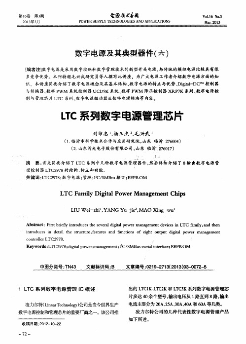
数字电源及其典型器件(六)——LTC系列数字电源管理芯片
_
.
摘
要: 首先简要介绍 了L T C 系列中几种数字电源管理器件 , 然后详细介 绍了 8 输 出数字电源管
理 控制 器 L T C2 9 7 8的 结构 、 特 点和 功 能。
关键词 : L T C 2 9 7 8 ; 数 字电 源 ; 管理 ; I 2 C / S MBu s 接 口; E E P ROM
中图分 类号 : T N 4 3
文献 标识 码 : B
文章编 号 : 0 2 1 9 - 2 7 1 3 ( 2 0 1 3) 0 3 - 0 0 7 2 — 5
1 L T C系列数 字电源管理 I C概述
凌力 尔特( L i n e a r T e c h n o l o g y ) 公 司是当今世界 生产
c o n t r o l l e r LTC2 9 78 . 。
Ke y wo r d s : L TC2 9 7 8 ; d i g i t a l p o we r ; ma na g e me n t ; I C/ S M Bu s s wr i l a i n t e r f a c e ; E E P R OM
i n t r o d u c e s i n d e t a i l t h e s t r u c t u r e , f e a ur t e s a n d f u n c t i o n s o f e i g h t o u t p u t ig d i ̄ p o we r m a n a g e me n t
一
L T C 2 9 7 0和 L T C 2 9 7 0 — 1 采用 4 a r m× 5 a r m的 2 4
个 内置 L D O,而 L T C 3 8 8 0 — 1 利 用一个 外部 5 V的
ltc3789芯片中文资料及推荐参数
ltc3789芯片中文资料及推荐参数LTC3789 是一款高性能、降压-升压型开关稳压控制器,可以在输入电压高于、低于或等于输出电压的情况下运作。
该器件运用了恒定频率、电流模式架构,故可提供一个高达600kHz 的可锁相频率,而一个输出电流反馈环路则提供了对电池充电的支持。
凭借4V 至38V (最大值为40V)的宽输入和输出范围以及工作区之间的无缝和低噪声转换,LTC3789 成为了汽车、电信和电池供电型系统的理想选择。
在降压或升压模式时,LTC3789 运用专有电流模式控制架构实现恒定频率工作,而且内置了4 个强大的N 沟道MOSFET 栅极驱动器。
LTC3789 还提供一个准确的恒定电流调节环路,用于在宽输入电压范围内调节输入或输出电流。
输入电流限制功能防止输入电源过载,输出电流限制为诸如电池充电器或LED 驱动器等稳定输出电流应用提供了非常容易的解决方案。
该器件在所有工作模式下为过压、过流和短路情况提供了故障保护。
此外,LTC3789 在停机时断开输入电压和输出电压的连接。
用户可以选择连续或脉冲跳跃模式,以最大限度地提高轻负载效率,并允许将IC 同步至一个外部时钟。
脉冲跳跃模式在轻负载条件下可实现最低的纹波,而强制连续模式则工作于一个恒定的频率以满足噪声敏感型应用的需要。
此外,LTC3789 具有可调软启动、电源良好输出,并在-40C 至125C 的工作结温范围内保持1.5% 的基准电压准确度。
当输出位于其设计设定点的10% 以内时,一个电源良好输出引脚将发生指示信号。
LTC3789 采用扁平的28 引脚4mm x 5mm QFN 封装和窄体SSOP 封装。
LTC3789引脚说明LTC3789引脚图1. VFB(PIN1/PIN26):误差放大器反馈引脚。
LTC3789收到的反馈电压来自于外部电阻分压器输出的电压。
2. SS(PIN2/PIN27):外部软启动输入引脚。
LTC3789调节VFB电压到较小的0.8V或SS 引脚上的电压。
ltc2954的用法
ltc2954的用法LTC2954是一款高性能电源管理芯片,广泛应用于各种电子设备中。
它具有多种功能,可以实现电源开关、电源监控和电源管理等功能,为电子设备的稳定运行提供了重要保障。
首先,LTC2954可以实现电源开关功能。
在很多电子设备中,为了节省能源和延长电池寿命,需要在设备不使用时自动关闭电源。
LTC2954可以通过控制外部开关管,实现电源的开关功能。
当设备不使用时,LTC2954会自动关闭电源,避免电池能量的浪费。
而当设备需要使用时,LTC2954会自动打开电源,保证设备正常运行。
其次,LTC2954还可以实现电源监控功能。
在电子设备中,电源的稳定性对设备的正常运行至关重要。
LTC2954可以监测电源的电压和电流,并及时反馈给控制系统。
当电源电压或电流异常时,LTC2954会发出警报信号,提醒用户或控制系统进行处理。
这样可以避免因电源问题导致的设备故障或损坏,保证设备的稳定运行。
此外,LTC2954还具有电源管理功能。
在一些特殊应用中,需要对电源进行精确控制,以满足设备的特定需求。
LTC2954可以通过外部控制信号,实现对电源的精确控制。
用户可以根据需要,通过控制LTC2954的工作模式和参数,实现对电源的灵活管理。
这样可以满足不同设备的特定需求,提高设备的性能和可靠性。
总之,LTC2954是一款功能强大的电源管理芯片,广泛应用于各种电子设备中。
它可以实现电源开关、电源监控和电源管理等多种功能,为设备的稳定运行提供了重要保障。
通过LTC2954的应用,可以有效节省能源、延长电池寿命,提高设备的性能和可靠性。
未来,随着科技的不断发展,LTC2954的用途将会更加广泛,为电子设备的发展带来更多的可能性。
LTC电源管理芯片
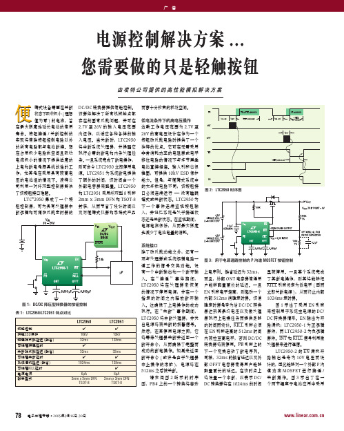
里被停用。一旦某个系统完成 了其断电操作,则其将能够把 KILL 引脚设定为低电平 ( 因而 立即关断电源 ),从而终止内部 1024ms 定时器。 图 1 示 出 了 采 用 EN 引 脚 来控制用于系统主电源的 DC/ DC 转换器情形。EN 输出为开 路漏极;LTC2950-1 为正逻辑 器件,而 LTC2950-2 为负逻辑 器件。INT 和 KILL 信号利用微 处理器来进行通信。 LTC2950-2 的 EN 漏 极 开 路 输 出 是 专 为 10V 电 压 而 设 计的,因此能够对一个外部 P 沟 道 功 率 MOSFET 进 行 接 通 / 关 断 操 作。 图 3 示 出 了 在 一 个两节锂离子电池应用中采用
LTC2951
� 10kV 128ms 32ms � 128ms � 6µA 2mm x 3mm DFN TSOT-8
上电序列。缺省延迟为 32ms, 而且,外部 ONT 电容器使得用 户能够配置更长的延迟。一旦 EN 引脚电平走高,则起动一个 内部 512ms 消隐定时器。该消 隐定时器是专为给 DC/DC 转换 器达到其最终电压以及微处理 器执行上电操任务而提供足够 的时间而设计。KILL 引脚必须 在 EN 引脚走高的 512ms 时间 内被拉至高电平,否则 DC/DC 转换器将被停用。PB 引脚上的 下一个变换启动了断电序列。 同样,32ms 的缺省延迟以及外 部 OFFT 电容器使得用户能够 配置更长的延迟。在该时点上 将设置一个中断,以表示 DC/ DC 转换器将在 1024ms 的时间
图 2:LTC2950 时序图
图 3:用于电源通路控制的 P 沟道 MOSFET 按钮控制
图 1:DC/DC 降压型转换器的按钮控制 表 1:LTC2950/LTC2951 特点对比
- 1、下载文档前请自行甄别文档内容的完整性,平台不提供额外的编辑、内容补充、找答案等附加服务。
- 2、"仅部分预览"的文档,不可在线预览部分如存在完整性等问题,可反馈申请退款(可完整预览的文档不适用该条件!)。
- 3、如文档侵犯您的权益,请联系客服反馈,我们会尽快为您处理(人工客服工作时间:9:00-18:30)。
而言十分珍贵的板级空间。 低电流条件下的高电压操作 这 款 工 作 电 压 范 围 为 2.7V 至 26V 的高电压设计在作为一个 按钮防反跳电路时提供了一个 独特的优点。它可在无需采用 非常消耗功率的电阻器或电平 移位电路的情况下与多节层叠 电池直接相连。输入引脚也很 稳固,可提供 10kV ESD 保护 能力。但是,与便携式系统中 的大多数电路不同,该按钮接 口必须连续运行 —没有睡眠 模式或关断状态。LTC2950 为 下一个事件连续监视按钮输 入,并记忆系统是处于接通状 态还是关断状态。在监视期间, 电源电流很低,从而最大限度 地减少了电池电量的消耗。 系统接口 除了防反跳功能之外,还有一 项与处理器或系统逻辑电路一 道 工 作 的 信 号 交 换 功 能。 设 有一个中断输出和一个断开输 入。 在“ 接 通 ” 事 件 期 间, LTC2950 将 在 处 理 器 未 恢 复 的情况下停用电源,并在一个 指定的时间之内释放断开输 入。这确保了上电操作的成功 执行。在“关断”事件期间, LTC2950 将中断处理器,并发 出电源将被关断的报警信号。 然后,在其停用电源之前,它 将等待处理器关断并返回一个 断开命令,从而确保了完整而 成功的断电操作。如果未返回 断开命令 ( 或许是由于处理器 中 止 操 作 的 缘 故 ), 电 源 将 在 512ms 之后被关断。 请参阅图 2 所示的时序 图,PB# 上的一个转换将启动
图 2:LTC2950 时序图
图 3:用于电源通路控制的 P 沟道 MOSFET 按钮控制
图 1:DC/DC 降压型转换器的按钮控制 表 1:LTC2950/LTC2951 特点对比
LTC2950
按钮控制 按钮ESD保护 接通防反跳延迟 (缺省) 可编程接通延时 关断防反跳延迟 (缺省) 可编程关断延时 系统停机延迟 (缺省) 可编程KILL延时 电源电流 封装型式 � 10kV 32ms � 32ms � 1024ms 6µA 2mm x 3mm DFN TSOT-8
里被停用。一旦某个系统完成 了其断电操作,则其将能够把 KILL 引脚设定为低电平 ( 因而 立即关断电源 ),从而终止内部 1024ms 定时器。 图 1 示 出 了 采 用 EN 引 脚 来控制用于系统主电源的 DC/ DC 转换器情形。EN 输出为开 路漏极;LTC2950-1 为正逻辑 器件,而 LTC2950-2 为负逻辑 器件。INT 和 KILL 信号利用微处理器来进行通信。 LTC2950-2 的 EN 漏 极 开 路 输 出 是 专 为 10V 电 压 而 设 计的,因此能够对一个外部 P 沟 道 功 率 MOSFET 进 行 接 通 / 关 断 操 作。 图 3 示 出 了 在 一 个两节锂离子电池应用中采用
图 7:接通 / 关断电源排序的按钮控制
注: 、 和 是凌特公司的注册商标。所有其 他商标均为其各自拥有者的产权。
电子工程专辑 • 2005年9月16日-30日
79
DC/DC 转换器提供使能控制。 该器件解决了所有机械触点都 存在的固有反跳问题,并可在 2.7V 至 26V 的 输 入 电 压 范 围 内运作,以适应各种各样的输 入电压。当关断时,LTC2950 将中断系统处理器,并提醒它 执行必需的断电和内务处理任 务。 一旦系统完成了断电操作, 则可命令 LTC2950 立即停用电 源。LTC2951 为系统断电提供 了额外的时间,该时间由一个 外部电容器来配置。LTC2950 和 LTC2951 采用纤巧型 8 引脚 2mm x 3mm DFN 和 TSOT-8 封装,从而节省了设计时间以 及对便携式仪器和手持式产品
78
电子工程专辑 • 2005年9月16日-30日
广 告
图 4:具有低电池电量监视器的 LDO 按钮控制
图 5:处理器停机时间有所延长的按钮控制
LTC2950-2 (EN) 来对一个用于 电源通路控制的外部 MOSFET 进行开关操作的情形。这使得 用户能够通过 PB 引脚电平的 变换来实现电源或后备电池与 其 负 载 的 连 接 / 断 接。INT 和 KILL 引脚通过一个阻性分压器 与 MOSFET 的输出端相连。于 是,当 INT 走低时,KILL 将被 拉至低电平,从而立即切断电 源。KILL 引脚还起一个电压监 视器的作用。当 VOUT 降至 6V 以下时,EN 引脚将在 30µ s 之 后被拉至高电平。 与前一个电路一样,图 4 中的电路也利用了用于 KILL 输 入的精准模拟比较器,因而它 可用作一个电压监视器。它由 微处理器的一个低漏电流漏极 开路输出来驱动。它还被连接 至一个负责监视电池电压 (V IN )
LTC2951
� 10kV 128ms 32ms � 128ms � 6µA 2mm x 3mm DFN TSOT-8
上电序列。缺省延迟为 32ms, 而且,外部 ONT 电容器使得用 户能够配置更长的延迟。一旦 EN 引脚电平走高,则起动一个 内部 512ms 消隐定时器。该消 隐定时器是专为给 DC/DC 转换 器达到其最终电压以及微处理 器执行上电操任务而提供足够 的时间而设计。KILL 引脚必须 在 EN 引脚走高的 512ms 时间 内被拉至高电平,否则 DC/DC 转换器将被停用。PB 引脚上的 下一个变换启动了断电序列。 同样,32ms 的缺省延迟以及外 部 OFFT 电容器使得用户能够 配置更长的延迟。在该时点上 将设置一个中断,以表示 DC/ DC 转换器将在 1024ms 的时间
的阻性分压器。当电池电压降 至 5.4V 以 下 时,KILL 引 脚 上 的电压将降至 0.6V 以下,而且
EN 引脚被迅速拉至低电平。所 示的 DC/DC 转换器在其 SHDN 引脚上具有一个内部上拉电流 : 因而无需在 EN 引脚上布设一个 上拉电阻器。 LTC2951 与 LTC2950 基本相 同,只是前者用可调接通定时 器换取一个可调 KILL 定时器。 图 5 示出了与图 1 大致相同的 电路,差异只是在于接通防反 跳时间在内部固定于 128ms, 而且,与 KILLT 引脚相连的外 部电容器使得提供给处理器以 完成其停机序列并释放 KILL 引 脚的时间从 128ms ( 缺省值 ) 延长至 339ms,如图 5 所示。 图 6:一个用于电源通路控制的双通道理想二极管的按钮控制 图 6 示出了电 池 与交 流 适 配 器 之 间 的 电 源 通 路 控 制。 按钮控制的应用范围并不 列。当所有电源均成功断电且 LTC4413 是一款专为减少发热、 仅限于电池供电型系统。具有 LTC2950 采用 P 沟道 MOSFET 压降、板级空间并保存电池使 多个电源以及苛刻的排序要求 断开电源时,DONE 引脚将把 用寿命而设计的双通道理想二 的大型系统可得益于简化的接 KILL 引脚驱动至低电平。 极管。对于需要一个理想二极 通 / 关断控制。图 7 示出了采用 便携式和非便携式设备 管“或”操作功能来实现负载 LTC2950 来控制一个与 4 个电 利用按钮控制来启动和停用电 均分或两个输入电源之间自动 源 ( 这些电源由 LTC2924 来排 源。 这 往 往 需 要 一 个 能 够 采 切换的应用而言,该器件是一 序 ) 相串联的 P 沟道 MOSFET 用 高 输 入 电 压 作 为 工 作 电 源 种理想的选择。虽然 LTC4413 的 情 形。 当 电 源 被 使 能 时, 的 纤 巧 型 低 电 流 解 决 方 案。 可 对 每 个 理 想 二 极 管 进 行 控 LTC2924 的 ON 引脚被拉至高 LTC2950 和 LTC2951 就提供了 制 存 取, 但 是 在 该 电 路 中, 电平以开始上电序列。对每个 这种解决方案,并且还可与处 LTC2950 的 EN 输出与每个输 输出进行监视,并由 DONE 输 理器相连接,以确保上电和断 入端相连,因而可同时起动两 出发出上电序列已成功完成的 电例行程序的正确执行。这些 个通道。INT 和 KILL 引脚连接 信 号。 这 将 释 放 LTC2950 的 器件采用纤巧型 2mm x 3mm 在一起,从而可在不需要进行 KILL 输入。当按钮命令系统断电 DFN 封装以及少量的可选外部 处理器信号交换的场合简化上 时,INT 引脚把 LTC2924 的 ON 元件,从而提供了简单而可靠 电 / 断电序列。 引脚拉至低电平以开始断电序 的按钮控制。
广 告
电源控制解决方案 ... 您需要做的只是轻触按钮
由凌特公司提供的高性能模拟解决方案
便
携式设备需要在关断 状态下吸收极小 ( 理想 值为零 ) 的电流,旨 在最大限度地延长电池的使用 寿命。按钮接通 / 关断控制的 实现将使除按钮控制电路以外 的所有电路都与电池断接。想 在占用极少电路板空间且吸收 电流极小的情况下提供适度的 上电和断电是颇具挑战性的工 作,尤其是在采用具有较高电 压的电池组的情况下。凌特公 司利用一对纤巧型控制器解决 了该按钮接口难题。 LTC ®2950 集 成 了 一 个 按 钮控制器,可为具有处理器中 断逻辑和可调防反跳定时器的