低功耗LVDS时钟扇出缓冲器
LVDS原理及设计指南
LVDS原理及设计指南LVDS(Low Voltage Differential Signaling)是一种低电压差分传输技术,常用于高速数据通信和时钟分配系统。
它通过使用两条平衡的信号线(一个正极和一个负极)来传输数据,以减少噪音干扰,提供更高的数据传输速率和更低的功耗。
LVDS的原理是将要传输的数据进行编码,然后在发送端将编码后的信号通过一个差分发射器发送出去。
在接收端,差分接收器将接收到的信号进行解码,并还原为原始数据。
差分发射器和差分接收器之间通过两条平衡的信号线相连,使得信号可以在传输过程中保持高的抗干扰能力。
为了实现高速数据传输和低功耗,设计LVDS系统时需要注意以下几点:1.选择合适的传输线:LVDS系统常用的传输线有两对铜排、双绞线和屏蔽电缆。
传输线的选择应根据系统需求和环境条件来确定,以保证信号传输的稳定性和可靠性。
2.保持信号的差分平衡:在设计LVDS系统时,传输线的长度和阻抗应保持一致,以保证差分信号的平衡性。
同时,在PCB设计中,需要采取合适的布线方式,如使用相邻层的信号层和地层进行屏蔽,以减少信号的串扰。
3.电源和地线的设计:为了保证LVDS系统的稳定性和可靠性,需要为差分发射器和差分接收器提供稳定的电源和地线。
一般应采用低噪声的电源和地线设计,并保持电源和地线与传输线相互独立,以防止互相干扰。
4.噪声抑制和滤波措施:在LVDS系统中,噪声干扰是一个常见的问题。
为了减少噪声的影响,可以采用电源滤波器、地线滤波器、抗干扰电容和电感等措施,以有效抑制噪声的干扰。
5.时钟分配的设计:对于需要传输时钟信号的LVDS系统,时钟分配的设计尤为重要。
时钟线应尽量短,以保证时钟信号的稳定性和准确性。
同时,需要采用低噪声的时钟源,并根据时钟分配的延时要求进行恰当的布线和抗干扰措施。
6.PCB设计布局:在LVDS系统的PCB设计中,需要合理规划和布局不同电路模块的位置,以减少信号的干扰和串扰。
BUFG,IBUFG,BUFGP,IBUFGDS等含义以及使用

BUFG,IBUFG,BUFGP,IBUFGDS等含义以及使用目前,大型设计一般推荐使用同步时序电路。
同步时序电路基于时钟触发沿设计,对时钟的周期、占空比、延时和抖动提出了更高的要求。
为了满足同步时序设计的要求,一般在FPGA设计中采用全局时钟资源驱动设计的主时钟,以达到最低的时钟抖动和延迟。
FPGA全局时钟资源一般使用全铜层工艺实现,并设计了专用时钟缓冲与驱动结构,从而使全局时钟到达芯片内部的所有可配置单元(CLB)、I/O单元(IOB)和选择性块RAM(Block Select RAM)的时延和抖动都为最小。
为了适应复杂设计的需要,Xilinx的FPGA中集成的专用时钟资源与数字延迟锁相环(DLL)的数目不断增加,最新的Virtex II器件最多可以提供16个全局时钟输入端口和8个数字时钟管理模块(DCM)。
与全局时钟资源相关的原语常用的与全局时钟资源相关的Xilinx器件原语包括:IBUFG、IBUFGDS、BUFG、BUFGP、BUFGCE、BUFGMUX、BUFGDLL和DCM等,如图1所示。
1. IBUFG即输入全局缓冲,是与专用全局时钟输入管脚相连接的首级全局缓冲。
所有从全局时钟管脚输入的信号必须经过IBUF元,否则在布局布线时会报错。
IBUFG支持AGP、CTT、GTL、GTLP、HSTL、LVCMOS、LVDCI、LVDS、LVPECL、LVTTL、PCI、PCIX和SSTL等多种格式的IO标准。
G 单2. IBUFGDS是IBUFG的差分形式,当信号从一对差分全局时钟管脚输入时,必须使用IBUFGDS作为全局时钟输入缓冲。
IBUFG支持BLVDS、LDT、LVDSEXT、LVDS、LVPECL和ULVDS等多种格式的IO标准。
3. BUFG是全局缓冲,它的输入是IBUFG的输出,BUFG的输出到达FPGA内部的IOB、CLB、选择性块RAM的时钟延迟和抖动最小。
4. BUFGCE是带有时钟使能端的全局缓冲。
Skyworks PCIe 时钟生成器和缓冲器系列应用指南说明书

AN781: Alternative Output Termination for Si5211x, Si5213x, Si5214x, Si5216x,Si522xx, Si5310x, Si5311x, and Si5315x PCIe Clock Generator and Buffer Families This application note is intended to provide optional, alternative output terminationsfor converting a low-power HCSL output clock from a Skyworks PCIe clock generatoror buffer device into a LVPECL, LVDS, or CML formatted clock. These optional termi-nations are particularly useful in applications that require both 100 MHz PCIe output clocks, as well as 100 MHz LVDS, LVPECL, or CML output clocks for FPGAs, SGMII,or other chipsets. Rather than using separate clock generators or oscillators to satisfy these system requirements, one can utilize a single-clock generator or buffer IC from Skyworks and employ different terminations on each output to achieve the desired results. It is relevant to note all Skyworks devices that provide HCSL PCIe outputs utilize low-power, push-pull buffers as opposed to constant current mode buffers. There are many advantages to using low-power, push-pull output buffers, including lower power consumption, elimination of external termination resistors, and overall reduction in total PCB area.KEY FEATURES OR KEY POINTS•Translate HCSL to LVPECL, LVDS or CML levels•Reduce Power Consumption•Simplify BOM AVL1. Conversion of HCSL Signals to LVPECL SignalsA low-power, push-pull HCSL output clock can be converted to either 2.5 V or 3.3 V LVPECL standards by using an output termination as shown in Figure 1.1 Termination Scheme for HCSL to LVPECL Conversion on page 2. Figure 1.2 Oscilloscope Measurement of LVPECL Conversion on page 2 shows the output clock at the measurement point indicated in Figure 1.1 Termination Scheme for HCSL to LVPECL Conversion on page 2. VCC supply is required to set the common mode voltage at the receiver end. Table 1.1 Resistor Selection for Different VCC Standards (LVPECL Signal Conversion) on page 3 lists the resistor selection based on VCC.GNDFigure 1.1. Termination Scheme for HCSL to LVPECL ConversionFigure 1.2. Oscilloscope Measurement of LVPECL ConversionTable 1.1. Resistor Selection for Different VCC Standards (LVPECL Signal Conversion)Table 1.2. Series Resistor Selection for PCIe Clock Generators and Buffers2. Conversion of HCSL Signals to LVDS SignalsOne can also convert a low-power, push-pull HCSL clock output to a 1.8 V, 2.5 V, or 3.3 V LVDS clock output. The recommended termination scheme is shown in Figure 2.1 Termination Scheme for Low-Power HCSL to LVDS Conversion(When Receiver has no Termination or Internal 100 Ω Termination) on page 4, with the corresponding oscilloscope measurement shown in Figure 2.2 Oscilloscope Measurement of LVDS Conversion(When Receiver has no Internal Termination) on page 4 (at the measurement point indicated in Figure 2.1 Termination Scheme for Low-Power HCSL to LVDS Conversion(When Receiver has no Termination or Internal 100 Ω Termination) on page 4).GNDFigure 2.1. Termination Scheme for Low-Power HCSL to LVDS Conversion(When Receiver has no Termination or Internal 100 Ω Termination)Figure 2.2. Oscilloscope Measurement of LVDS Conversion(When Receiver has no Internal Termination)The swing will be reduced by 50% by an internal or external termination (the signal will be similar to the signal seen in Figure 2.4 Oscilloscope Measurement of LVDS Conversion(When Receiver has Internal or External 100 Ω Termination) on page 5). If the receiver does not have an internal 100 Ω termination,an external 100 Ω termination may be added, as shown in Figure 2.3 Termination Scheme for Low-Power HCSL to LVDS Conversion (When Receiver has no Internal 100 Ω Termination) on page 5.GNDFigure 2.3. Termination Scheme for Low-Power HCSL to LVDS Conversion(When Receiver has no Internal 100 Ω Termination)Figure 2.4. Oscilloscope Measurement of LVDS Conversion (When Receiver has Internal or External 100 Ω Termination)The resistor selection guide for different VCC values at the receiver end is given in Table 2.1 Resistor Selection on page 5.Table 2.1. Resistor SelectionFor series resistor selection of PCIe clock generators and buffers, see Table 1.2 Series Resistor Selection for PCIe Clock Generators and Buffers on page 3.Buffer Families • Conversion of HCSL Signals to CML Signals (AC Coupled to Receivers)3. Conversion of HCSL Signals to CML Signals (AC Coupled to Receivers)AC coupling is the recommended method for converting low-power HCSL signals to CML. The receiver should be able to generate the references needed to generate the common mode for CML signals. The recommended schematic is shown in Figure 3.1 Termination Scheme for HCSL to CML AC Coupling on page 6. It is also important to note that many CML receivers come with internal 50 Ωterminations to VCC, as shown in Figure 3.2 Typical CML Receiver Circuit Structure on page 6. Such internal terminations can reduce the signal swing by 50%.Figure 3.1. Termination Scheme for HCSL to CML AC CouplingFigure 3.2. Typical CML Receiver Circuit StructureBuffer Families • Conclusion4. ConclusionThis application note details methods in which low-power HCSL output clocks from the Si5211x, Si5213x, Si5214x, Si5216x, Si5310x, Si5311x, Si5315x, and Si522xx device families can be used to drive receivers that use other differential formats, specifically LVPECL, LVDS, and CML standards.Copyright © 2021 Skyworks Solutions, Inc. All Rights Reserved.Information in this document is provided in connection with Skyworks Solutions, Inc. (“Skyworks”) products or services. These materials, including the information contained herein, are provided by Skyworks as a service to its customers and may be used for informational purposes only by the customer. Skyworks assumes no responsibility for errors or omissions in these materials or the information contained herein. Skyworks may change its documentation, products, services, specifications or product descriptions at any time, without notice. Skyworks makes no commitment to update the materials or information and shall have no responsibility whatsoever for conflicts, incompatibilities, or other difficulties arising from any future changes.No license, whether express, implied, by estoppel or otherwise, is granted to any intellectual property rights by this document. Skyworks assumes no liability for any materials, products or information provided hereunder, including the sale, distribution, reproduction or use of Skyworks products, information or materials, except as may be provided in Skyworks’ Terms and Conditions of Sale.THE MATERIALS, PRODUCTS AND INFORMATION ARE PROVIDED “AS IS” WITHOUT WARRANTY OF ANY KIND, WHETHER EXPRESS, IMPLIED, STATUTORY, OR OTHERWISE, INCLUDING FITNESS FOR A PARTICULAR PURPOSE OR USE, MERCHANTABILITY, PERFORMANCE, QUALITY OR NON-INFRINGEMENT OF ANY INTELLECTUAL PROPERTY RIGHT; ALL SUCH WARRANTIES ARE HEREBY EXPRESSLY DISCLAIMED. SKYWORKS DOES NOT WARRANT THE ACCURACY OR COMPLETENESS OF THE INFORMATION, TEXT, GRAPHICS OR OTHER ITEMS CONTAINED WITHIN THESE MATERIALS. SKYWORKS SHALL NOT BE LIABLE FOR ANY DAMAGES, INCLUDING BUT NOT LIMITED TO ANY SPECIAL, INDIRECT, INCIDENTAL, STATUTORY, OR CONSEQUENTIAL DAMAGES, INCLUDING WITHOUT LIMITATION, LOST REVENUES OR LOST PROFITS THAT MAY RESULT FROM THE USE OF THE MATERIALS OR INFORMATION, WHETHER OR NOT THE RECIPIENT OF MATERIALS HAS BEEN ADVISED OF THE POSSIBILITY OF SUCH DAMAGE.Skyworks products are not intended for use in medical, lifesaving or life-sustaining applications, or other equipment in which the failure of the Skyworks products could lead to personal injury, death, physical or environmental damage. Skyworks customers using or selling Skyworks products for use in such applications do so at their own risk and agree to fully indemnify Skyworks for any damages resulting from such improper use or sale.Customers are responsible for their products and applications using Skyworks products, which may deviate from published specifications as a result of design defects, errors, or operation of products outside of published parameters or design specifications. Customers should include design and operating safeguards to minimize these and other risks. Skyworks assumes no liability for applications assistance, customer product design, or damage to any equipment resulting from the use of Skyworks products outside of Skyworks’ published specifications or parameters.Skyworks, the Skyworks symbol, Sky5®, SkyOne ®, SkyBlue™, Skyworks Green™, Clockbuilder ®, DSPLL ®, ISOmodem ®, ProSLIC ®, and SiPHY ® are trademarks or registered trademarks of Skyworks Solutions, Inc. or its subsidiaries in the United States and other countries. Third-party brands and names are for identification purposes only and are the property of their respective owners. Additional information, including relevant terms and conditions, posted at , are incorporated by reference.Portfolio/ia/timingSW/HW/CBProQuality/qualitySupport & Resources/supportClockBuilder ProCustomize Skyworks clock generators, jitter attenuators and networksynchronizers with a single tool. With CBPro you can control evaluationboards, access documentation, request a custom part number, export for in-system programming and more!/CBPro。
低偏移,1到4 LVCMOS LVTTL到3.3V LVPECL分频缓冲器 ICS8535-01说明
Low Skew, 1-to-4 LVCMOS/LVTTL-to-3.3V LVPECL Fanout BufferICS8535-01General DescriptionThe ICS8535-01is a low skew,high performance 1-to-4LVCMOS/LVTTL-to-3.3V LVPECL fanout buffer.The ICS8535-01has two single ended clock inputs.the single ended clock input accepts LVCMOS or LVTTL input levels and translate them to 3.3V LVPECL levels.The clock enable is internally synchronized to eliminate runt clock pulses on the output during asynchronous assertion/deassertion of the clock enable pin.Guaranteed output and part-to-part skew characteristics make the ICS8535-01ideal for those applications demanding well defined performance and repeatability.6 7 89 1019 20 18 17 1612345V CC Q2nQ2V CC nc1314151211Q3nQ3V CC V EE CLK_ENQ 0n Q 0Q 1n Q 1V C Cn cC L K 0C L K _S E LC L K 1n c12345678910Q0nQ0V CC Q1nQ1Q2nQ2V CC Q3nQ320191817161514131211V EE CLK_EN CLK_SELCLK0nc CLK1nc nc nc V CCICS8535-0120-Lead VFQFN4mm x 4mm x 0.9body packageK PackageTop ViewICS8535-0120-Lead TSSOP4.4mm x 6.5mm x 0.92body packageG PackageTop ViewPin AssignmentFeatures•Four differential 3.3V LVPECL outputs•Selectable CLK0or CLK1inputs for redundant and multiple frequency fanout applications•CLK0or CLK1can accept the following input levels:LVCMOS or LVTTL•Maximum output frequency:266MHz•T ranslates LVCMOS and LVTTL levels to 3.3V LVPECL levels •Output skew:30ps (maximum)•Part-to-part skew:250ps (maximum)•Propagation delay:1.9ns (maximum)•Additive phase jitter,RMS:<0.09ps (typical)•3.3V operating supply•0°C to 70°C ambient operating temperature •Lead-free (RoHS 6)packagingBlock DiagramICS8535-01 DATA SHEETPin Descriptions and CharacteristicsTable 1.Pin Descriptions 1Table 2.Pin CharacteristicsICS8535-01 DATA SHEETFigure 1.Table 3A.Control Input Function TableCLK0, CLK1CLK_ENnQ0:nQ3Q0:Q3Table 3B.Clock Input Function TableICS8535-01 DATA SHEETAbsolute Maximum RatingsNOTE:Stresses beyond those listed under Absolute Maximum Ratings may cause permanent damage to the device.These ratings are stress specifications only.Functional operation of product at these conditions or any conditions beyond those listed in the DC Electrical Characteristics or AC Characteristics is not implied.Exposure to absolute maximum rating conditions for extended periods may affect product reliability.DC Electrical CharacteristicsTable 4A.Power Supply DC Characteristics,V CC =3.3V±5%,T A =0°C to 70°CTable 4B.LVCMOS/LVTTL DC Characteristics,V CC =3.3V±5%,T A =0°C to 70°CTable 4C.LVPECL DC Characteristics,V CC =3.3V±5%,T A =0°C to 70°CCCICS8535-01 DATA SHEETAC CharacteristicsTable5.AC Characteristics,V CC =3.3V±5%,T A =0°C to 70°C 1The part does not add jitter.NOTE 2:Measured from the V CC /2of the input to the differential output crosspoint.NOTE 3:Defined as skew between outputs at the same supply voltage and with equal load conditions.Measured at the output differentialcrosspointsNOTE 4:This parameter is defined in accordance with JEDEC Standard 65.NOTE 5:Defined as skew between outputs on different devices operating at the same supply voltages and with equal load ingthe same type of inputs on each device,the outputs are measured at the differential crosspoints.NOTE 6:Driving only one input clock.ICS8535-01 DATA SHEETAdditive Phase JitterThe spectral purity in a band at a specific offset from the fundamental compared to the power of the fundamental is called the dBc Phase Noise.This value is normally expressed using a Phase noise plot and is most often the specified plot in many applications.Phase noise is defined as the ratio of the noise power present in a 1Hz band at a specified offset from the fundamental frequency to the power value of the fundamental.This ratio is expressed in decibels (dBm)or a ratioof the power in the 1Hz band to the power in the fundamental.When the required offset is specified,the phase noise is called a dBc value,which simply means dBm at a specified offset from the fundamental.By investigating jitter in the frequency domain,we get a betterunderstanding of its effects on the desired application over the entire time record of the signal.It is mathematically possible to calculate an expected bit error rate given a phase noise plot.As with most timing specifications,phase noise measurements have issues.The primary issue relates to the limitations of the equipment.Often the noise floor of the equipment is higher than the noise floorof the device.This is illustrated above.The device meets the noise floor of what is shown,but can actually be lower.The phase noise is dependent on the input source and measurement equipment.N o i s e P o w e r (d B c /H z )Offset Frequency (Hz)Input/Output Additive Phase Jitter at 156.25MHz =0.09ps (typical)1k10k100k1M10M-190-180-170-160-150-140-130-120-110-100-90-80-70-60-50-40-30-20-100100MICS8535-01 DATA SHEET Parameter MeasurementInformation3.3V Output Load Test CircuitOutput SkewPropagation DelayPart-to-Part SkewOutput Rise/Fall TimeOutput Duty Cycle/Pulse Width/PeriodICS8535-01 DATA SHEETApplications InformationRecommendations for Unused Input PinsInputs:CLK InputFor applications not requiring the use of a clock input,it can be left floating.Though not required,but for additional protection,a 1k Ωresistor can be tied from the CLK input to ground.LVCMOS Control PinsAll control pins have internal pullups;additional resistance is not required but can be added for additional protection.A 1k Ωresistor can be used.Outputs:LVPECL OutputsAll unused LVPECL outputs can be left floating.We recommend that there is no trace attached.Both sides of the differential output pair should either be left floating or terminated.Termination for 3.3V LVPECL OutputsThe clock layout topology shown below is a typical termination for LVPECL outputs.The two different layouts mentioned are recommended only as guidelines.The differential output is a low impedance follower output thatgenerate ECL/LVPECL compatible outputs.Therefore,terminating resistors (DC current path to ground)or current sources must be used for functionality.These outputs are designed to drive 50Ωtransmission lines.Matched impedance techniques should be used to maximize operating frequency and minimize signal distortion.Figure 2A and Figure 2B show two different layouts which arerecommended only as guidelines.Other suitable clock layouts may exist and it would be recommended that the board designerssimulate to guarantee compatibility across all printed circuit and clock component process variations.Figure 2A.3.3V LVPECL Output Termination Figure 2B.3.3V LVPECL Output TerminationICS8535-01 DATA SHEETSchematic ExampleFigure 3shows a schematic example of the ICS8535-01.In this example,the CLK0input is selected.The decoupling capacitors should be physically located near the power pin.For ICS8535-01,the unused clock outputs can be left floating.Figure 3.ICS8535-01Schematic ExampleICS8535-01 DATA SHEETPower ConsiderationsThis section provides information on power dissipation and junction temperature for the ICS8535-01.Equations and example calculations are also provided.1.Power Dissipation.The total power dissipation for the ICS8535-01is the sum of the core power plus the power dissipated in the load(s).The following is the power dissipation for V CC =3.3V +5%=3.465V ,which gives worst case results.NOTE:Please refer to Section 3for details on calculating power dissipated in the load.•Power (core)MAX =V CC_MAX *I EE_MAX =3.465V *50mA =173.25mW •Power (outputs)MAX =30mW/Loaded Output pairIf all outputs are loaded,the total power is 4*30mW =120mWTotal Power_MAX (3.465V ,with all outputs switching)=173.25mW +120mW =293.25mW 2.Junction Temperature.Junction temperature,Tj,is the temperature at the junction of the bond wire and bond pad and directly affects the reliability of the device.The maximum recommended junction temperature is 125°C.The equation for Tj is as follows:Tj =θJA *Pd_total +T A Tj =Junction T emperatureθJA =Junction-to-Ambient Thermal ResistancePd_total =T otal Device Power Dissipation (example calculation is in section 1above)T A =Ambient T emperatureIn order to calculate junction temperature,the appropriate junction-to-ambient thermal resistance θJA must be used.Assuming a moderate air flow of 200linear feet per minute and a multi-layer board,the appropriate value is 66.6°C/W per T able 6A below.Therefore,Tj for an ambient temperature of 70°C with all outputs switching is:70°C +0.293W *66.6°C/W =89.5°C.This is below the limit of 125°C.This calculation is only an example.Tj will obviously vary depending on the number of loaded outputs,supply voltage,air flow and the type of board (single layer or multi-layer).Table 6A.Thermal Resistance θfor 20-Lead TSSOP ,Forced ConvectionNOTE:Most modern PCB designs use multi-layered boards.The data in the second row pertains to most designs.Table 6B.θvs.Air Flow Table for 20-Lead VFQFNICS8535-01 DATA SHEET 3.Calculationsand Equations.The purpose of this section is to derive the power dissipated into the load.LVPECL output driver circuit and termination are shown in Figure4.Figure4.LVPECL Driver Circuit and TerminationT o calculate worst case power dissipation into the load,use the following equations which assume a50Ωload,and a termination voltage of V CC–2V.•For logic high,V OUT=V OH_MAX=V CC_MAX–0.9V(V CC_MAX–V OH_MAX)=0.9V•For logic low,V OUT=V OL_MAX=V CO_MAX–1.7V(V CC_MAX–V OL_MAX)=1.7VPd_H is power dissipation when the output drives high.Pd_L is the power dissipation when the output drives low.Pd_H=[(V OH_MAX–(V CC_MAX–2V))/R L]*(V CC_MAX–V OH_MAX)=[(2V-(V CC_MAX–V OH_MAX))/R L]*(V CC_MAX–V OH_MAX)=[(2V-0.9V)/50Ω]*0.9V=19.8mWPd_L=[(V OL_MAX–(V CC_MAX–2V))/R L]*(V CC_MAX–V OL_MAX)=[(2V–(V CC_MAX–V OL_MAX))/R L]*(V CC_MAX–V OL_MAX)=[(2V–1.7V)/50Ω]*1.7V=10.2mWT otal Power Dissipation per output pair=Pd_H+Pd_L=30mWICS8535-01 DATA SHEETReliability InformationNOTE:Most modern PCB designs use multi-layered boards.The data in the second row pertains to most designs.Table 7B.θvs.Air Flow Table for 20-Lead VFQFNTransistor CountThe transistor count for the IS8535-01is 412.Table 7A.θJA vs.Air Flow Table for a 20-Lead TSSOPICS8535-01 DATA SHEETPackage Outline and Package DimensionsICS8535-01 DATA SHEETPackage Outline and Package Dimensions (continued)Package Outline -K Suffix for 20-Lead VFQFNReference Document:JEDEC Publication 95,MO-220NOTE:The drawing and dimension data originate from IDT package outline drawing PSC-4170,rev03.1.Dimensions and tolerances conform to ASME Y14.5M-19942.All dimensions are in millimeters.All angles are in degrees.3.N is the total number of terminals.4.All specifications comply with JEDEC MO-220.Table 9.Package Dimensions for 20-Lead VFQFNICS8535-01 DATA SHEETOrdering InformationTable10.Ordering InformationICS8535-01 DATA SHEETRevision History SheetICS8535-01 DATA SHEETDISCLAIMER Integrated Device Technology, Inc. (IDT) and its subsidiaries reserve the right to modify the products and/or specifications described herein at any time and at IDT’s sole discretion. All information in this document, including descriptions of product features and performance, is subject to change without notice. Performance specifications and the operating parameters of the described products are determined in the independent state and are not guaranteed to perform the same way when installed in customer products. The information contained herein is provided without representation or warranty of any kind, whether express or implied, including, but not limited to, the suitability of IDT’s products for any particular purpose, an implied warranty of merchantability, or non-infringement of the intellectual property rights of others. This document is presented only as a guide and does not convey any license under intellectual property rights of IDT or any third parties.IDT’s products are not intended for use in applications involving extreme environmental conditions or in life support systems or similar devices where the failure or malfunction of an IDT product can be reasonably expected to significantly affect the health or safety of users. Anyone using an IDT product in such a manner does so at their own risk, absent an express, written agreement by IDT.While the information presented herein has been checked for both accuracy and reliability, Integrated Device Technology (IDT) assumes no responsibility for either its use or for the infringement of any patents or other rights of third parties, which would result from its use. No other circuits, patents, or licenses are implied. This product is intended for use in normal commercial applications. Any other applications, such as those requiring extended temperature ranges, high reliability or other extraordinary environmental requirements are not recommended without additional processing by IDT. IDT reserves the right to change any circuitry or specifications without notice. IDT does not authorize or warrant any IDT product for use in life support devices or critical medical instruments.Corporate Headquarters6024 Silver Creek Valley Road San Jose, CA 95138 USASales1-800-345-7015 or 408-284-8200 Fax: Tech Supportemail:**************Corporate HeadquartersTOYOSU FORESIA, 3-2-24 Toyosu,Koto-ku, Tokyo 135-0061, Japan Contact InformationFor further information on a product, technology, the most up-to-date version of a document, or your nearest sales office, please visit:/contact/TrademarksRenesas and the Renesas logo are trademarks of Renesas Electronics Corporation. All trademarks and registered trademarks are the property of their respective owners.IMPORTANT NOTICE AND DISCLAIMERRENESAS ELECTRONICS CORPORATION AND ITS SUBSIDIARIES (“RENESAS”) PROVIDES TECHNICAL SPECIFICATIONS AND RELIABILITY DATA (INCLUDING DATASHEETS), DESIGN RESOURCES (INCLUDINGREFERENCE DESIGNS), APPLICATION OR OTHER DESIGN ADVICE, WEB TOOLS, SAFETY INFORMATION, AND OTHER RESOURCES “AS IS” AND WITH ALL FAULTS, AND DISCLAIMS ALL WARRANTIES, EXPRESS OR IMPLIED, INCLUDING, WITHOUT LIMITATION, ANY IMPLIED WARRANTIES OF MERCHANTABILITY, FITNESS FOR A PARTICULAR PURPOSE, OR NON-INFRINGEMENT OF THIRD PARTY INTELLECTUAL PROPERTY RIGHTS.These resources are intended for developers skilled in the art designing with Renesas products. You are solely responsible for (1) selecting the appropriate products for your application, (2) designing, validating, and testing your application, and (3) ensuring your application meets applicable standards, and any other safety, security, or other requirements. These resources are subject to change without notice. Renesas grants you permission to use these resources only for development of an application that uses Renesas products. Other reproduction or use of these resources is strictly prohibited. No license is granted to any other Renesas intellectual property or to any third party intellectual property. Renesas disclaims responsibility for, and you will fully indemnify Renesas and its representatives against, any claims,damages, costs, losses, or liabilities arising out of your use of these resources. Renesas' products are provided only subject to Renesas' Terms and Conditions of Sale or other applicable terms agreed to in writing. No use of any Renesas resources expands or otherwise alters any applicable warranties or warranty disclaimers for these products.(Rev.1.0 Mar 2020)。
时钟扇出缓冲器与时钟分配分频器
时钟扇出缓冲器与时钟分配分频器下载提示:该文档是本店铺精心编制而成的,希望大家下载后,能够帮助大家解决实际问题。
文档下载后可定制修改,请根据实际需要进行调整和使用,谢谢!本店铺为大家提供各种类型的实用资料,如教育随笔、日记赏析、句子摘抄、古诗大全、经典美文、话题作文、工作总结、词语解析、文案摘录、其他资料等等,想了解不同资料格式和写法,敬请关注!Download tips: This document is carefully compiled by this editor. I hope that after you download it, it can help you solve practical problems. The document can be customized and modified after downloading, please adjust and use it according to actual needs, thank you! In addition, this shop provides you with various types of practical materials, such as educational essays, diary appreciation, sentence excerpts, ancient poems, classic articles, topic composition, work summary, word parsing, copy excerpts, other materials and so on, want to know different data formats and writing methods, please pay attention!时钟扇出缓冲器与时钟分配分频器在数字电路中起着至关重要的作用。
Si53360 61 62 65 低噪声 LVCMOS 分输出时钟缓冲器说明书
Si53360/61/62/65 Data Sheet Low-Jitter, LVCMOS Fanout Clock Buffers with up to 12 outputsand Frequency Range from dc to 200 MHzThe Si53360/61/62/65 family of LVCMOS fanout buffers is ideal for clock/data distri-bution and redundant clocking applications. The family utilizes Skyworks advanced CMOS technology to fanout clocks from dc to 200 MHz with guaranteed low additive jitter, low skew, and low propagation delay variability. Built-in LDOs deliver high PSRR performance and eliminates the need for external components simplifying low jitter clock distribution in noisy environments.The CMOS buffers are available in multiple configurations with 8 outputs(Si53360/61/65), or dual banks of 6 outputs each (Si53362). These buffers can be paired with the Si534x clock generators and Si5xx oscillators to deliver end-to-end clock tree performance.KEY FEATURES•Low additive jitter: 120 fs rms•Built-in LDOs for high PSRR performance •Up to 12 LVCMOS Outputs from LVCMOS inputs•Frequency range: dc to 200 MHz •Multiple configuration options•Dual Bank option•2:1 Input MUX option•RoHS compliant, Pb-free •Temperature range: –40 to +85 °CCLK0CLK1CLK_SEL CLKTable of Contents1. Ordering Guide (3)2. Functional Description (4)2.1 LVCMOS Input Termination (4)2.2 Input Mux (4)2.3 Output Clock Termination Options (5)2.4 AC Timing Waveforms (6)2.5 Power Supply Noise Rejection (6)2.6 Typical Phase Noise Performance: Single-Ended Input Clock (7)2.7 Input Mux Noise Isolation (8)3. Electrical Specifications (9)4. Detailed Block Diagrams (12)5. Si5336x Pin Descriptions (15)5.1 Si53360 Pin Descriptions (15)5.2 Si53361 Pin Descriptions (17)5.3 Si53362 Pin Descriptions (19)5.4 Si53365 Pin Descriptions (21)6. Package Outline (22)6.1 16-Pin TSSOP Package (22)6.2 16-Pin QFN Package (24)6.3 24-Pin QFN Package (25)7. PCB Land Pattern (26)7.1 16-Pin TSSOP Land Pattern (26)7.2 16-Pin QFN Land Pattern (27)7.3 24-Pin QFN Land Pattern (29)8. Top Markings (31)8.1 Si53360/65 Top Markings (31)8.2 Si53361 Top Marking (32)8.3 Si53362 Top Marking (33)9. Revision History (34)Si53360/61/62/65 Data Sheet • Ordering Guide1. Ordering GuideTable 1.1. Si5336x Ordering Guide2. Functional DescriptionThe Si53360/61/62/65 are a family of low-jitter, low skew, fixed format (LVMCOS) buffers. These devices are available in multiple configurations customized for the end application (refer to 1. Ordering Guide for more details on configurations).2.1 LVCMOS Input TerminationThe table below summarizes the various ac- and dc-coupling options supported by the LVCMOS device, and the figure shows the recommended input clock termination.Table 2.1. LVCMOS Input Clock OptionsV DDCMOSDriverNote: Value for Rs should be chosen so that the total source impedance matches the characteristic impedance of the PCB trace.Figure 2.1. Recommended Input Clock Termination2.2 Input MuxThe Si53360-61/62 provide two clock inputs for applications that need to select between one of two clock sources. The CLK_SEL pin selects the active clock input. The following table summarizes the input and output clock based on the input mux settings.Table 2.2. Input Mux Logic2.3 Output Clock Termination OptionsThe recommended output clock termination options are shown below. Unused outputs should be left unconnected.CMOSNote:Rs = 33 ohm for 3.3 V and 2.5 V operation.Rs = 0 ohm for 1.8 V operation.Figure 2.2. LVCMOS Output Termination2.4 AC Timing WaveformsQ N Q MT SKT SKT PLHT RT FQQCLK QT PHLOutput-Output SkewPropagation DelayRise/Fall TimeVPP/2VPP/280% VPP 20% VPPFigure 2.3. AC Timing Waveforms2.5 Power Supply Noise RejectionThe device supports on-chip supply voltage regulation to reject power supply noise and simplify low-jitter operation in real-world envi-ronments. This feature enables robust operation alongside FPGAs, ASICs and SoCs and may reduce board-level filtering requirements.See “AN491: Power Supply Rejection for Low-Jitter Clocks ” for more information.2.6 Typical Phase Noise Performance: Single-Ended Input ClockEach of the phase noise plots superimposes Source Jitter and Total Jitter on the same diagram.•Source Jitter - Reference clock phase noise (measured Single-ended to PNA).•Total Jitter - Combined source and clock buffer phase noise measured as a single-ended output to the phase noise analyzer and integrated from 12 kHz to 20 MHz. For more information, see 3. Electrical Specifications.Note: To calculate the total RMS phase jitter when adding a buffer to your clock tree, use the root-sum-square (RSS).measured hereFigure 2.4. Single-ended Measurement Method The following figure shows three phase noise plots superimposed on the same diagram.Figure 2.5. Total Jitter Single-Ended Input (156.25 MHz)2.7 Input Mux Noise IsolationThe input clock mux is designed to minimize crosstalk between the CLK0 and CLK1. This improves phase jitter performance when clocks are present at both the CLK0 and CLK1 inputs. The following figure shows a measurement of the input mux’s noise isolation.Figure 2.6. Input Mux Noise Isolation (Single-ended Input Clock, 16QFN Package)3. Electrical SpecificationsTable 3.1. Recommended Operating ConditionsTable 3.2. Input Clock SpecificationsV DD = 1.8 V ± 5%, 2.5 V ± 5%, or 3.3 V ± 10%, T A = –40 to 85 °CTable 3.3. DC Common Characteristics (CLK_SEL, OEx) V DD = 1.8 V ± 5%, 2.5 V ± 5%, or 3.3 V ± 10%, T A = –40 to 85 °CTable 3.4. Output Characteristics (LVCMOS) V DD = 1.8 V ± 5%, 2.5 V ± 5%, or 3.3 V ± 10%, T A = –40 to 85 °CTable 3.5. AC CharacteristicsV DD = 1.8 V ± 5%, 2.5 V ± 5%, or 3.3 V ± 10%, T A = –40 to 85 °CTable 3.6. Additive JitterTable 3.7. Thermal ConditionsTable 3.8. Absolute Maximum Ratings4. Detailed Block DiagramsCLK0CLK1 CLK_SELQ0Q1Q2Q3Q4Q5Q6Q7Si53361 - 16-QFN 3x3 mmVDDO (Si53361 only)Figure 4.1. Si53360 and Si53361 Block DiagramQ7Q6Q8OEBVDDOBQ10Q9Q11Q1Q0Q2OEA VDDOA Q4Q3Q5CLK0CLK1CLK_SELFigure 4.2. Si53362 Block DiagramCLKFigure 4.3. Si53365 Block Diagram5. Si5336x Pin Descriptions5.1 Si53360 Pin DescriptionsCLK0CLK1Q2Q1GND Q6Q5Q3VDD Q0VDD Q7GND OE Q4CLK_SELFigure 5.1. Si53360 Pin Descriptions Table 5.1. Si53360 16-TSSOP Pin Descriptions5.2 Si53361 Pin DescriptionsO EC L K 1Q0Q1Q 2Q 3Q 4Q 5Q6C L K _S E LQ7VDDGND VDDO C L K 0GNDFigure 5.2. Si53361 Pin Descriptions Table 5.2. Si53361 16-QFN Pin Descriptions5.3 Si53362 Pin DescriptionsVDDN CN CN C CLK_SELQ2Q3V D D O A Q 4Q 5Q 6Q 7V D D O BQ11Q8N CQ9Q1OEA C L K 1OEB Q0C L K 0Q10Figure 5.3. Si53362 Pin Descriptions Table 5.3. Si53362 24-QFN Pin Descriptions5.4 Si53365 Pin DescriptionsQ6Q7VDD GND VDD Q2GND Q4OE Q0Q3VDD GND CLK Q5Q1Figure 5.4. Si53365 Pin Descriptions Table 5.4. Si53365 16-TSSOP Pin DescriptionsSi53360/61/62/65 Data Sheet • Si5336x Pin Descriptions6. Package Outline6.1 16-Pin TSSOP PackageFigure 6.1. 16-Pin TSSOP PackageTable 6.1. 16-Pin TSSOP Package DimensionsTable 6.2. 16-QFN Package DimensionsTable 6.3. 24-QFN Package Dimensions7. PCB Land Pattern7.1 16-Pin TSSOP Land PatternFigure 7.1. 16-Pin TSSOP Land PatternTable 7.1. 16-Pin TSSOP Land Pattern Dimensions7.2 16-Pin QFN Land PatternFigure 7.2. 16-Pin QFN Land PatternTable 7.2. 16-QFN Land Pattern Dimensions7.3 24-Pin QFN Land PatternFigure 7.3. 24-Pin QFN Land PatternTable 7.3. 24-QFN Land Pattern Dimensions8. Top Markings8.1 Si53360/65 Top MarkingsFigure 8.1. Si53360 Top Marking Figure 8.2. Si53365 Top MarkingTable 8.1. Si53360/65 Top Marking ExplanationMark Method:LaserFont Size: 2.0 Point (0.71 mm)Right-JustifiedLine 1 Marking:Device Part Number53360 for Si53360, 53365 for Si53365Line 2 Marking:TTTTTT = Mfg Code Manufacturing Code from the Assembly Purchase Order form. Line 3 Marking YY = Year, WW = WorkCorresponds to the year and work week of the mold date.WeekFigure 8.3. Si53361 Top MarkingTable 8.2. Si53361 Top Marking ExplanationMark Method:LaserFont Size: 2.0 Point (0.71 mm) Cen-ter-alignedLine 1 Marking:Device Part Number3361 for Si53361Line 2 Marking:TTTTTT = Mfg Code Manufacturing Code from the Assembly Purchase Order form.Line 3 Marking YY = Year, WW = WorkWeek Corresponds to the year and work week of the mold date.Figure 8.4. Si53362 Top MarkingTable 8.3. Si53362 Top Marking ExplanationMark Method:LaserFont Size: 2.0 Point (0.71 mm)Right-justifiedLine 1 Marking:Device Part Number53362 for Si53362Line 2 Marking:TTTTTT = Mfg Code Manufacturing Code from the Assembly Purchase Order form.Line 3 Marking YY = Year, WW = WorkWeek Corresponds to the year and work week of the mold date.9. Revision HistoryRevision 1.3December, 2018•Changed CLK_SEL from pull-down resistor to pull-up resistor.•Updated output state to low when OE pin is asserted low on Si53365.Revision 1.2December, 2016•Introduced Si53361 and Si53362 new products.•Merged Si53360/65 datasheets with the new products to create a single LVCMOS buffer datasheet.•Added Core supply current spec at multiple supply voltages.•Added “Internal pull-down resistor” typical spec.Copyright © 2021 Skyworks Solutions, Inc. All Rights Reserved.Information in this document is provided in connection with Skyworks Solutions, Inc. (“Skyworks”) products or services. These materials, including the information contained herein, are provided by Skyworks as a service to its customers and may be used for informational purposes only by the customer. Skyworks assumes no responsibility for errors or omissions in these materials or the information contained herein. Skyworks may change its documentation, products, services, specifications or product descriptions at any time, without notice. Skyworks makes no commitment to update the materials or information and shall have no responsibility whatsoever for conflicts, incompatibilities, or other difficulties arising from any future changes.No license, whether express, implied, by estoppel or otherwise, is granted to any intellectual property rights by this document. Skyworks assumes no liability for any materials, products or information provided hereunder, including the sale, distribution, reproduction or use of Skyworks products, information or materials, except as may be provided in Skyworks’ Terms and Conditions of Sale.THE MATERIALS, PRODUCTS AND INFORMATION ARE PROVIDED “AS IS” WITHOUT WARRANTY OF ANY KIND, WHETHER EXPRESS, IMPLIED, STATUTORY, OR OTHERWISE, INCLUDING FITNESS FOR A PARTICULAR PURPOSE OR USE, MERCHANTABILITY, PERFORMANCE, QUALITY OR NON-INFRINGEMENT OF ANY INTELLECTUAL PROPERTY RIGHT; ALL SUCH WARRANTIES ARE HEREBY EXPRESSLY DISCLAIMED. SKYWORKS DOES NOT WARRANT THE ACCURACY OR COMPLETENESS OF THE INFORMATION, TEXT, GRAPHICS OR OTHER ITEMS CONTAINED WITHIN THESE MATERIALS. SKYWORKS SHALL NOT BE LIABLE FOR ANY DAMAGES, INCLUDING BUT NOT LIMITED TO ANY SPECIAL, INDIRECT, INCIDENTAL, STATUTORY, OR CONSEQUENTIAL DAMAGES, INCLUDING WITHOUT LIMITATION, LOST REVENUES OR LOST PROFITS THAT MAY RESULT FROM THE USE OF THE MATERIALS OR INFORMATION, WHETHER OR NOT THE RECIPIENT OF MATERIALS HAS BEEN ADVISED OF THE POSSIBILITY OF SUCH DAMAGE.Skyworks products are not intended for use in medical, lifesaving or life-sustaining applications, or other equipment in which the failure of the Skyworks products could lead to personal injury, death, physical or environmental damage. Skyworks customers using or selling Skyworks products for use in such applications do so at their own risk and agree to fully indemnify Skyworks for any damages resulting from such improper use or sale.Customers are responsible for their products and applications using Skyworks products, which may deviate from published specifications as a result of design defects, errors, or operation of products outside of published parameters or design specifications. Customers should include design and operating safeguards to minimize these and other risks. Skyworks assumes no liability for applications assistance, customer product design, or damage to any equipment resulting from the use of Skyworks products outside of Skyworks’ published specifications or parameters.Skyworks, the Skyworks symbol, Sky5®, SkyOne ®, SkyBlue™, Skyworks Green™, Clockbuilder ®, DSPLL ®, ISOmodem ®, ProSLIC ®, and SiPHY ® are trademarks or registered trademarks of Skyworks Solutions, Inc. or its subsidiaries in the United States and other countries. Third-party brands and names are for identification purposes only and are the property of their respective owners. Additional information, including relevant terms and conditions, posted at , are incorporated by reference.Portfolio/ia/timing SW/HW /CBPro Quality /quality Support & Resources /support ClockBuilder ProCustomize Skyworks clock generators,jitter attenuators and networksynchronizers with a single tool. WithCBPro you can control evaluationboards, access documentation, requesta custom part number, export for in-system programming and more!/CBPro。
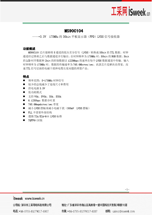
杭州瑞盟科技有限公司MS90C104 30bit平板显示器LVDS信号接收器说明书
2013.08.12
共9页 第6页
图 4.锁相环设置时间
MS90C104
图 5.接收器状态
Vdiff=(RxIN+)-(RxIN-),……(RxCLKIN+)-(RxCLKIN-)
图 6.并行 TTL 输出数据与 LVDS 输入数据匹配关系
Previous Cycle
Next Cycle
RCLK RL4
1.4W
电学特性
符号 VIH VIL VOH
VOL
IIN IOS
参数 输入高电平 输入低电平 输出高电平
输出低电平
输入电流 输出短路电流
条件
Min
2.0
GND
IOH = -4mA(data) 2.4 IOH = -8mA(clock) IOL = 4mA(data) IOL = 8mA(clock)
-3-
版本号:1.2
2013.08.12
共9页 第3页
MS90C104
推荐工作条件
电源电压(VCC) CMOS/TTL 输入电压 CMOS/TTL 输出电压 LVDS 接收输入电压 结点温度 温度范围 瞬间耐温(焊接,4 秒) 最大功耗(25℃) MS90C104
-0.3V - 4.0V -0.3V - (VCC+0.3V) -0.3V - (VCC+0.3V) -0.3V - (VCC+0.3V) +150℃ -40℃ - 100℃ +260℃
RX0/7/14/21/28
RX1/8/15/22/29
RX2/9/16/23/30 RX3/10/17/24/31 RX4/11/18/25/32 RX5/12/19/26/33 RX6/13/20/27/34
LVDS信号的工作原理和特点 (2)
LVDS信号的工作原理和特点LVDS(Low Voltage Differential Signaling)是一种低电压差分信号传输技术,它通过在发送端将信号分成两路相反的电平来传输数据,接收端通过比较这两路信号的差值来恢复原始数据。
LVDS信号具有较高的抗干扰能力和传输速率,被广泛应用于各种数字信号传输领域。
一、LVDS信号的工作原理1. 发送端工作原理:LVDS发送端将输入的数字信号经过编码和差分放大处理,生成两路相反的电平信号。
这两路信号的差值表示了原始数据的逻辑状态,例如低电平差值表示“0”,高电平差值表示“1”。
发送端还会根据协议要求添加时钟信号,以确保接收端能够正确解析数据。
2. 接收端工作原理:LVDS接收端通过比较两路相反的电平信号的差值来恢复原始数据。
如果差值大于一个阈值,则被判定为“1”,如果差值小于阈值,则被判定为“0”。
接收端还会根据时钟信号对数据进行同步处理,以确保数据的准确传输和解析。
二、LVDS信号的特点1. 低电压差分传输:LVDS信号采用低电平差分传输技术,相较于单端传输,具有更好的抗干扰能力和传输稳定性。
差分信号的传输方式能够减少电磁辐射和噪声干扰,提高信号传输的可靠性和抗干扰能力。
2. 高传输速率:LVDS信号传输速率高,可以达到几百兆比特每秒(Gbps)甚至更高。
这使得LVDS广泛应用于高速数据传输领域,如显示器接口、视频传输、高速通信等。
3. 低功耗:LVDS信号传输时采用较低的电压和电流,因此具有较低的功耗。
这对于需要长距离传输或者挪移设备来说非常重要,可以延长电池寿命并提高系统效率。
4. 高抗干扰能力:由于采用了差分传输和编码技术,LVDS信号具有较强的抗干扰能力。
它能够有效抵御来自外部电磁场、噪声和干扰源的影响,确保信号传输的稳定性和可靠性。
5. 长距离传输:LVDS信号可以在较长的距离范围内传输,通常可以达到几十米甚至更远的距离。
这使得LVDS在需要远距离传输的应用中具有优势,如医疗设备、工业自动化等领域。