时钟缓冲器基础知识---文本资料
时钟的知识点归纳总结
时钟的知识点归纳总结时钟是人类生活中不可或缺的工具之一,我们在日常生活中常常需要依靠时钟来获取准确的时间信息。
以下是关于时钟的一些知识点的归纳总结。
一、时钟的基本原理:1.基于机械原理的时钟:机械钟通过摆锤的摆动来驱动时针、分针和秒针的运动,从而显示时间。
2.基于电子原理的时钟:电子时钟通过晶体振荡器产生稳定的频率信号,然后通过锁相环电路将该信号转化为秒脉冲,从而驱动时、分、秒指针的运动。
二、时钟的种类:1.机械钟:机械钟是最早发展起来的一种钟表,其内部由一系列齿轮和摆锤组成,通过齿轮的传动来驱动时、分、秒指针运动。
2.石英钟:石英钟是一种利用石英晶体的压电效应来产生电压信号的钟表,具有精确的时间显示和较长的使用寿命。
3.原子钟:原子钟是以原子核或原子的共振频率作为时间基准的钟表,具有非常高的精确度和稳定性。
三、时钟的工作原理:1.机械钟的工作原理:机械钟内部装有一个重物,称为摆锤,通过摆锤的摆动来驱动齿轮系统,从而驱动时、分、秒指针的运动。
2.石英钟的工作原理:石英钟内部有一个石英晶体,应用于其上的电压会使晶体发生压电效应,进而产生稳定的频率信号,该信号经过计数和分频后用于驱动指针运动。
3.原子钟的工作原理:原子钟使用原子核或原子的共振频率作为时间基准,通常使用铯或铯原子,通过测量铯原子的共振频率来计算出准确的时间。
四、时钟的精准度:1.机械钟的精准度:机械钟的精准度一般较低,通常为每天准确率在数秒左右。
2.石英钟的精准度:石英钟的精准度要比机械钟高得多,通常为每天准确率在数十毫秒左右。
3.原子钟的精准度:原子钟的精准度非常高,通常为每天准确率在纳秒或皮秒级别。
五、时钟的应用:1.家用时钟:家用时钟主要用于在家庭生活中显示时间,通常由石英钟或机械钟组成。
2.办公室时钟:办公室时钟用于在办公环境中显示时间,通常会安装在墙上,以便员工方便查看时间。
3.公共场所时钟:公共场所时钟用于在公共场所如火车站、机场、购物中心等显示时间,以便公众准确掌握时间信息。
日常时钟相关知识点归纳

日常时钟相关知识点归纳日常时钟相关知识点主要包括时钟的基本构造、时钟的工作原理、不同类型的时钟、时钟的使用和维护等内容。
一、时钟的基本构造时钟由时钟机芯和表盘组成。
时钟机芯包括发条、主轴、齿轮、指针和摆轮等部件,用于传递时间信息。
表盘通常由数字或标志性刻度表示时间。
二、时钟的工作原理时钟机芯根据不同的设计原理,可以分为机械时钟、电子时钟和原子钟等类型。
机械时钟依靠发条的弹力和传动装置来驱动指针的运动;电子时钟通过电路和晶振来产生稳定的振荡信号,驱动数字或指针的显示;原子钟则利用原子的振荡频率作为计时基准,具有极高的精度和稳定度。
三、不同类型的时钟1.机械时钟:常见的挂钟、座钟等属于机械时钟,其工作原理是通过发条的弹力和齿轮传动来驱动指针的运动。
机械时钟需要定期上发条来提供动力。
2.电子时钟:电子时钟利用电路和晶振来产生稳定的振荡信号,驱动数字或指针的显示。
电子时钟通常使用电池或外部电源供电,具有较高的精度和稳定性。
3.原子钟:原子钟利用原子的振荡频率作为计时基准,具有极高的精度和稳定性。
原子钟通常用于科学研究和精密测量领域。
四、时钟的使用和维护1.校准时间:时钟的准确性和精度需要定期校准。
可以通过与标准时间源(如电波时钟、互联网时间服务器等)同步来校准时钟。
2.更换电池:电子时钟使用电池供电,需要定期更换电池以确保正常工作。
3.清洁维护:时钟表盘和机芯的清洁和维护可以延长时钟的使用寿命和保持良好的工作状态。
可以使用柔软的布擦拭,避免使用化学清洁剂。
4.防止冲击:时钟机芯内部的齿轮和零件非常精密,避免将时钟暴露在剧烈振动或冲击下,以免损坏时钟。
以上是日常时钟相关的基本知识点。
时钟作为一种时间工具,准确显示时间对我们的生活和工作非常重要,定期的维护和保养可以保证时钟的正常运行和使用寿命。
微光半导体 2012年 时钟缓冲器设计指南说明书
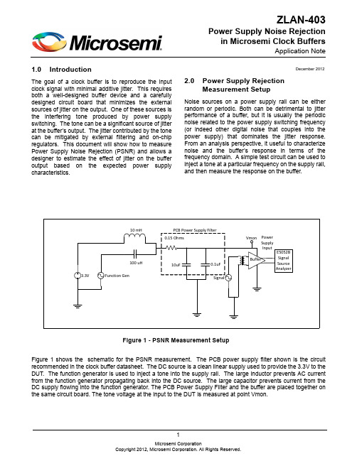
11.0 IntroductionThe goal of a clock buffer is to reproduce the input clock signal with minimal additive jitter. This requires both a well-designed buffer device and a carefully designed circuit board that minimizes the external sources of jitter on the output. One of these sources is the interfering tone produced by power supply switching. The tone can be a significant source of jitter at the buffer’s output. The jitter contributed by the tone can be mitigated by external filtering and on-chip regulators. This document will show how to measure Power Supply Noise Rejection (PSNR) and allows a designer to estimate the effect of jitter on the buffer output based on the expected power supply characteristics.2.0 Power Supply RejectionMeasurement SetupNoise sources on a power supply rail can be either random or periodic. Both can be detrimental to jitter performance of a buffer, but it is usually the periodic noise related to the power supply switching frequency (or indeed other digital noise that couples into the power supply) that dominates the jitter response.From an analysis perspective, it useful to characterize noise and the buffer’s response in terms of the frequency domain. A simple test circuit can be used to inject a tone at a particular frequency on the supply rail,and then measure the response on the buffer.December 2012ZLAN-403Power Supply Noise Rejection in Microsemi Clock BuffersApplication NoteFigure 1 shows the schematic for the PSNR measurement. The PCB power supply filter shown is the circuit recommended in the clock buffer datasheet. The DC source is a clean linear supply used to provide the 3.3V to the DUT. The function generator is used to inject a tone into the supply rail. The large inductor prevents AC current from the function generator propagating back into the DC source. The large capacitor prevents current from the DC supply flowing into the function generator. The PCB Power Supply Filter and the buffer are placed together on the same circuit board. The tone voltage at the input to the DUT is measured at point Vmon.Figure 1 - PSNR Measurement Setup3.0 PSNR Measurement ResultsUsing this test setup, a tone at a particular frequency is generated, and the effect on the output signal is captured by the Agilent E5052B Signal Source Analyzer. The signal source analyzer is configured with its "Spurious" option set to display spur power in dBc (decibels relative to the carrier). The magnitude of the tone or spur is shown on the phase noise plot. The PSNR is defined as the ratio of the output tone power to the carrier power. Figure 2 shows an example of 100 kHz power supply tone on a 125MHz input signal. The power of the tone at cursor 1 is shown in the first line of the text displayed in the plot: -77.4356 dBc. This is the PSNR of the buffer for this tone frequency.Figure 2 - Effect of Power Supply Tone on Buffer Output -- Phase NoiseTable 1 presents the additive jitter associated with a power supply tone at various frequencies for a 1:4 LVPECLclock buffer at room temperature. The carrier frequency in this case is 125 MHz, and the amplitude of the ripple isfixed at 25 mVpp at the DUT. The additive jitter is calculated from Equation 1. The buffer shows very goodrejection of power supply noise. Note that the additive jitter varies in a non-linear fashion with tone frequency.Where:PSNR is the magnitude of the tone power relative to the carrier in dBc.Fc is the frequency of the carrier in Hz.Jtone rms is the additive rms jitter due to the tone.It is difficult to fix the ripple amplitude at greater than 25 mVpp at higher frequencies, as the board power filter and decoupling capacitors tend to shunt the ripple to ground (which is their intended function). Practically, this limits the upper frequency to about 500 kHz.Measurements show that the additive jitter due to the tone at the output of the buffer is proportional to the amplitude of the tone at the input of the buffer. However, the constant of proportion is different for different tone frequencies.A plot of additive jitter vs input voltage for a 100 kHz tone is shown in Figure 3. From the graph, the amount of additive jitter can be determined based on the amplitude of the 100 kHz ripple.Table 1 - Power Supply Rejection at various frequency offsets with a carrier Frequency of 125 MHzFrequency Offset(kHz)Amplitude of Tone at Power Supply Input(mV pp)Power of Tone at Buffer Output relative to Carrier (PSNR in dBc)Additive Jitter due to Power Supply Tone(fs rms)10025-77.923120025-74.135530025-73.637440025-76.128150025-72.6423Jtone rms 10PSNR 20---------------2π×Fc×----------------------------=Equation 14.0 Additive Jitter and PSNRIt is useful to understand the impact of a particular power supply tone on the buffer’s output in terms of its contribution to additive jitter. Total jitter at the buffer’s output is given by Equation 2, with the assumption that the noise contributed by the tone is significantly above the random noise floor.Where:Jin rms is the random jitter on the input signal, with any contribution from spurs on the input removed,Jadd rms is the random additive noise that the buffer contributes,Jtone rms is the additive jitter contributed by the tone.Also, in the case where there is no power supply tone, the equation reduces to:Figure 3 - Additive Jitter vs Input Ripple Amplitude (mVpp)Jtotal rms Jin rms 2Jadd rms 2Jtone rms2++=Equation 2Jtone rms can be calculated from Equation 1 as stated earlier.As an example, consider a 125 MHz signal source with a random jitter of 200 fs rms between 12 kHz and 20 MHz.This signal is fed to the input of a clock distribution buffer which has an additive jitter of 110 fs rms at 125 MHz in the same band. In the absence of any power supply tones, the total random jitter output from the buffer will be given byEquation 3, , or 228 fs rms.Now assume a power supply tone is applied, and that its contribution can be seen on a phase noise plot of the buffer’s output as a spur with -85 dBc magnitude. This is the PSNR. The contribution from the tone in terms of jitter is given by Equation 1, and results in about 101 fs rms. Therefore, the total rms random jitter, found from Equation2, is , or 250 fs rms.Using the above equations, it is possible to plot a graph of the total jitter vs additive jitter contributed by a tone. For example consider a case in which the input jitter is 100 fs, the additive jitter from the buffer is 110 fs. Figure 4shows a plot of the total jitter vs increasing additive jitter due to power supply tone. The input jitter and additive jitter dominate the total jitter up to about 200 fs, then the rising jitter contributed by the tone begins to dominate.Jtotal rms Jin rms 2Jadd rms2+=Equation 320021102+200211021012++Figure 4 - Total Jitter vs Tone Contribution5.0 Designing for Power Supply RejectionThe PCB power supply filtering also contributes to overall Power Supply Rejection. Figure 5 shows the ideal transfer function of the filter components outlined in Figure 1. The 3dB frequency is given by , which is about 100kHz.The total Power Supply Noise Rejection is a combination of the attenuation due to the filter and the attenuation due to the buffer’s intrinsic PSNR.To appropriately manage power supply tones, the following jitter budgeting procedure can be used: •The total jitter allowed at the output must be defined.•The additive jitter of the buffer (J add ) and the expected jitter of the input signal (J in ) should be established.•The maximum jitter allowed to be contributed from a tone is then given from a derivative of Equation 2:•The maximum jitter is translated into a maximum tone voltage at the input of the buffer using a plot of additive jitter vs. input power supply ripple, as in Figure 3.•The maximum voltage at the buffer’s input is translated to the maximum ripple voltage on the power supply using Figure 5.For example, consider a system with a Jin of 300 fs rms and a Jadd of 110 fs rms (at 125 MHz). The maximum tolerable jitter at the output is 500 fs rms. From Equation 2, we have Jtone = 384 fs rms (maximum). Assume the concerning tone is generated by the power supply’s switching frequency, which is 100 kHz. From Figure 3, it can be seen that the maximum voltage on the input ripple must be less than ~40 mVpp. From Figure 3, at 100 kHz, the PCB filtering circuit attenuation factor is about 0.7. Therefore the ripple on the power supply must be less than 40mVpp/0.7 = 57 mVpp to achieve the 500 fs rms budget at the output. This is relatively easily achieved as most power supplies limit ripple below 30 mV pp.12πRC ()⁄Figure 5 - Transfer Function of Power Supply FilterJtone rms Jtotal rms 2Jin rms 2–Jadd rms 2–=6.0 ConclusionPower supply selection is an important consideration in low-jitter clock buffer design. To achieve the desired jitter targets, the board designer needs to consider the periodic voltage components on the supply rail, the PCB power supply filter design, and the clock buffer’s intrinsic power supply rejection. Microsemi clock buffers provide robust intrinsic power supply rejection. When they are used with the recommended power supply filter, significant attenuation of power supply ripple can be achieved. This allows board designers a wide degree of flexibility in power supply selection, while still maintaining the output jitter targets.Information relating to products and services furnished herein by Microsemi Corporation or its subsidiaries (collectively “Microsemi”) is believed to be reliable. However, Microsemi assumes no liability for errors that may appear in this publication, or for liability otherwise arising from the application or use of any suchinformation, product or service or for any infringement of patents or other intellectual property rights owned by third parties which may result from such application or use. Neither the supply of such information or purchase of product or service conveys any license, either express or implied, under patents or other intellectual property rights owned by Microsemi or licensed from third parties by Microsemi, whatsoever. Purchasers of products are also hereby notified that the use of product in certain ways or in combination with Microsemi, or non-Microsemi furnished goods or services may infringe patents or other intellectual property rights owned by Microsemi.This publication is issued to provide information only and (unless agreed by Microsemi in writing) may not be used, applied or reproduced for any purpose nor form part of any order or contract nor to be regarded as a representation relating to the products or services concerned. The products, their specifications, services and other information appearing in this publication are subject to change by Microsemi without notice. No warranty or guarantee express or implied is made regarding the capability, performance or suitability of any product or service. Information concerning possible methods of use is provided as a guide only and does not constitute any guarantee that such methods of use will be satisfactory in a specific piece of equipment. It is the user’s responsibility to fully determine the performance and suitability of any equipment using such information and to ensure that any publication or data used is up to date and has not been superseded.Manufacturing does not necessarily include testing of all functions or parameters. These products are not suitable for use in any medical and other products whose failure to perform may result in significant injury or death to the user. All products and materials are sold and services provided subject to Microsemi’s conditions of sale which are available on request.Purchase of Microsemi’s I 2C components conveys a license under the Philips I 2C Patent rights to use these components in an I 2C System, provided that the system conforms to the I 2C Standard Specification as defined by Philips.Microsemi, ZL, and combinations thereof, VoiceEdge, VoicePort, SLAC, ISLIC, ISLAC and VoicePath are trademarks of Microsemi Corporation.TECHNICAL DOCUMENTATION - NOT FOR RESALEFor more information about all Microsemi productsvisit our Web Site at。
微晟半导体 ZL40200 低噪声高频精密 LVPECL 双输出时钟缓冲器数据表说明书

1FeaturesInputs/Outputs •Accepts differential or single-ended input •LVPECL, LVDS, CML, HCSL, LVCMOS •Two precision LVPECL outputs •Operating frequency up to 750 MHzPower •Options for 2.5 V or 3.3 V power supply •Core current consumption of 49 mA•On-chip Low Drop Out (LDO) Regulator for superior power supply rejectionPerformance •Ultra low additive jitter of 39 fs RMSApplications•General purpose clock distribution •Low jitter clock trees •Logic translation•Clock and data signal restoration•Wired communications: OTN, SONET/SDH, GE, 10 GE, FC and 10G FC•PCI Express generation 1/2/3 clock distribution •Wireless communications•High performance microprocessor clock distributionApril 2014Figure 1 - Functional Block DiagramZL40200Precision 1:2 LVPECL Fanout BufferData SheetOrdering InformationZL40200LDG1 16 Pin QFN TraysZL40200LDF116 Pin QFN Tape and ReelMatte TinPackage size: 3 x 3 mm-40o C to +85o CTable of ContentsFeatures . . . . . . . . . . . . . . . . . . . . . . . . . . . . . . . . . . . . . . . . . . . . . . . . . . . . . . . . . . . . . . . . . . . . . . . . . . . . . . . . . 1 Inputs/Outputs . . . . . . . . . . . . . . . . . . . . . . . . . . . . . . . . . . . . . . . . . . . . . . . . . . . . . . . . . . . . . . . . . . . . . . . . .1 Power . . . . . . . . . . . . . . . . . . . . . . . . . . . . . . . . . . . . . . . . . . . . . . . . . . . . . . . . . . . . . . . . . . . . . . . . . . . . . . . .1 Performance . . . . . . . . . . . . . . . . . . . . . . . . . . . . . . . . . . . . . . . . . . . . . . . . . . . . . . . . . . . . . . . . . . . . . . . . . . .1 Applications . . . . . . . . . . . . . . . . . . . . . . . . . . . . . . . . . . . . . . . . . . . . . . . . . . . . . . . . . . . . . . . . . . . . . . . . . . . . . 1 Change Summary . . . . . . . . . . . . . . . . . . . . . . . . . . . . . . . . . . . . . . . . . . . . . . . . . . . . . . . . . . . . . . . . . . . . . . . . . 41.0 Package Description . . . . . . . . . . . . . . . . . . . . . . . . . . . . . . . . . . . . . . . . . . . . . . . . . . . . . . . . . . . . . . . . . . . .52.0 Pin Description. . . . . . . . . . . . . . . . . . . . . . . . . . . . . . . . . . . . . . . . . . . . . . . . . . . . . . . . . . . . . . . . . . . . . . . . .53.0 Functional Description . . . . . . . . . . . . . . . . . . . . . . . . . . . . . . . . . . . . . . . . . . . . . . . . . . . . . . . . . . . . . . . . . .63.1 Clock Inputs. . . . . . . . . . . . . . . . . . . . . . . . . . . . . . . . . . . . . . . . . . . . . . . . . . . . . . . . . . . . . . . . . . . . . . . . .63.2 Clock Outputs . . . . . . . . . . . . . . . . . . . . . . . . . . . . . . . . . . . . . . . . . . . . . . . . . . . . . . . . . . . . . . . . . . . . . .113.3 Device Additive Jitter. . . . . . . . . . . . . . . . . . . . . . . . . . . . . . . . . . . . . . . . . . . . . . . . . . . . . . . . . . . . . . . . .153.4 Power Supply . . . . . . . . . . . . . . . . . . . . . . . . . . . . . . . . . . . . . . . . . . . . . . . . . . . . . . . . . . . . . . . . . . . . . .163.4.1 Sensitivity to power supply noise. . . . . . . . . . . . . . . . . . . . . . . . . . . . . . . . . . . . . . . . . . . . . . . . . . .163.4.2 Power supply filtering. . . . . . . . . . . . . . . . . . . . . . . . . . . . . . . . . . . . . . . . . . . . . . . . . . . . . . . . . . . .163.4.3 PCB layout considerations. . . . . . . . . . . . . . . . . . . . . . . . . . . . . . . . . . . . . . . . . . . . . . . . . . . . . . . .164.0 AC and DC Electrical Characteristics . . . . . . . . . . . . . . . . . . . . . . . . . . . . . . . . . . . . . . . . . . . . . . . . . . . . .175.0 Performance Characterization . . . . . . . . . . . . . . . . . . . . . . . . . . . . . . . . . . . . . . . . . . . . . . . . . . . . . . . . . . .206.0 Typical Behavior . . . . . . . . . . . . . . . . . . . . . . . . . . . . . . . . . . . . . . . . . . . . . . . . . . . . . . . . . . . . . . . . . . . . . .217.0 Package Thermal Characteristics . . . . . . . . . . . . . . . . . . . . . . . . . . . . . . . . . . . . . . . . . . . . . . . . . . . . . . . .238.0 Mechanical Drawing . . . . . . . . . . . . . . . . . . . . . . . . . . . . . . . . . . . . . . . . . . . . . . . . . . . . . . . . . . . . . . . . . . .24List of FiguresFigure 1 - Functional Block Diagram . . . . . . . . . . . . . . . . . . . . . . . . . . . . . . . . . . . . . . . . . . . . . . . . . . . . . . . . . . . . 1 Figure 2 - Pin Connections . . . . . . . . . . . . . . . . . . . . . . . . . . . . . . . . . . . . . . . . . . . . . . . . . . . . . . . . . . . . . . . . . . . 5 Figure 3 - LVPECL Input DC Coupled Thevenin Equivalent . . . . . . . . . . . . . . . . . . . . . . . . . . . . . . . . . . . . . . . . . . 6 Figure 4 - LVPECL Input DC Coupled Parallel Termination. . . . . . . . . . . . . . . . . . . . . . . . . . . . . . . . . . . . . . . . . . . 7 Figure 5 - LVPECL Input AC Coupled Termination . . . . . . . . . . . . . . . . . . . . . . . . . . . . . . . . . . . . . . . . . . . . . . . . . 7 Figure 6 - LVDS Input DC Coupled . . . . . . . . . . . . . . . . . . . . . . . . . . . . . . . . . . . . . . . . . . . . . . . . . . . . . . . . . . . . . 8 Figure 7 - LVDS Input AC Coupled . . . . . . . . . . . . . . . . . . . . . . . . . . . . . . . . . . . . . . . . . . . . . . . . . . . . . . . . . . . . . 8 Figure 8 - CML Input AC Coupled . . . . . . . . . . . . . . . . . . . . . . . . . . . . . . . . . . . . . . . . . . . . . . . . . . . . . . . . . . . . . . 9 Figure 9 - HCSL Input AC Coupled . . . . . . . . . . . . . . . . . . . . . . . . . . . . . . . . . . . . . . . . . . . . . . . . . . . . . . . . . . . . . 9 Figure 10 - CMOS Input DC Coupled Referenced to VDD/2. . . . . . . . . . . . . . . . . . . . . . . . . . . . . . . . . . . . . . . . . 10 Figure 11 - CMOS Input DC Coupled Referenced to Ground . . . . . . . . . . . . . . . . . . . . . . . . . . . . . . . . . . . . . . . . 10 Figure 12 - Simplified Output Driver. . . . . . . . . . . . . . . . . . . . . . . . . . . . . . . . . . . . . . . . . . . . . . . . . . . . . . . . . . . . 11 Figure 13 - LVPECL Basic Output Termination . . . . . . . . . . . . . . . . . . . . . . . . . . . . . . . . . . . . . . . . . . . . . . . . . . . 11 Figure 14 - LVPECL Parallel Output Termination. . . . . . . . . . . . . . . . . . . . . . . . . . . . . . . . . . . . . . . . . . . . . . . . . . 12 Figure 15 - LVPECL Parallel Thevenin-Equivalent Output Termination. . . . . . . . . . . . . . . . . . . . . . . . . . . . . . . . . 12 Figure 16 - LVPECL AC Output Termination for Externally Terminated LVPECL Inputs . . . . . . . . . . . . . . . . . . . . 13 Figure 17 - LVPECL AC Output Termination for Internally Terminated LVPECL Inputs. . . . . . . . . . . . . . . . . . . . . 13 Figure 18 - LVPECL AC-Coupled Output Termination for CML Inputs. . . . . . . . . . . . . . . . . . . . . . . . . . . . . . . . . . 14 Figure 19 - Additive Jitter. . . . . . . . . . . . . . . . . . . . . . . . . . . . . . . . . . . . . . . . . . . . . . . . . . . . . . . . . . . . . . . . . . . . 15 Figure 20 - Decoupling Connections for Power Pins. . . . . . . . . . . . . . . . . . . . . . . . . . . . . . . . . . . . . . . . . . . . . . . 16 Figure 21 - Differential Voltage Parameter. . . . . . . . . . . . . . . . . . . . . . . . . . . . . . . . . . . . . . . . . . . . . . . . . . . . . . . 18 Figure 22 - Input To Output Timing . . . . . . . . . . . . . . . . . . . . . . . . . . . . . . . . . . . . . . . . . . . . . . . . . . . . . . . . . . . . 19Change SummaryPage ItemChange1Applications Added PCI Express clock distribution.5Pin Description Added exposed pad to Pin Description.Removed 22 O hm series resistors from Figure 3 and 4.These resistor s are not required; however there is no impact to performance if the resistors are included.6, 7Figure 3 and Figure 413Figure 16Corrected LVPECL interface circuit.18Figure 21Below are the changes from the February 2013 ti the April 2014 issue:Page Item Change7Figure 4Changed text to indicate the circuit is not recommended for VDD_driver=2.5V.7Figure 5Changed pull-up and pull-down resistors from 2kOhm to 100 Ohm.Below are the changes from the November 2012 issue to the February 2013 issue:Clarification of V ID and V OD.The device is packaged in a 16 pin QFN1416642NCvddNCN Cc l k _pvddgndNCo u t 1_no u t 1_po u t 0_n81210o u t 0_pc l k _nN CNCgndFigure 2 - Pin Connections2.0 Pin DescriptionPin Description Pin # Name Description1, 4clk_p, clk_n,Differential Input (Analog Input). Differential input signals.12, 11, 10, 9out0_p, out0_n out1_p, out1_n Differential Output (Analog Output). Differential outputs.8, 13vdd Positive Supply Voltage. 2.5V DC or 3.3 V DC nominal.5, 16gnd Ground. 0 V.2, 3, 6, 7, 14, 15NCNo Connection. Leave unconnected.Exposed Pad Device GND .The ZL40200 is an LVPECL clock fanout buffer with two identical output clock drivers capable of operating at frequencies up to 750MHz.Inputs to the ZL40200 are externally terminated to allow use of precision termination components and to allow full flexibility of input termination. The ZL40200 can accept DC coupled LVPECL or LVDS and AC coupled LVPECL, LVDS, CML or HCSL input signals; single ended input signals can also be accepted. A pin compatible device with internal termination is also available.The ZL40200 is designed to fan out low-jitter reference clocks for wired or optical communications applications while adding minimal jitter to the clock signal. An internal linear power supply regulator and bulk capacitors minimize additive jitter due to power supply noise. The device operates from 2.5V+/-5% or 3.3V+/-5% supply. Its operation is guaranteed over the industrial temperature range -40°C to +85°C.The device block diagram is shown in Figure 1; its operation is described in the following sections.3.1 Clock InputsThe device can accept LVPECL, LVDS, CML, HCSL and single-ended inputs.Figure 3 - LVPECL Input DC Coupled Thevenin EquivalentFigure 4 - LVPECL Input DC Coupled Parallel TerminationFigure 5 - LVPECL Input AC Coupled TerminationFigure 6 - LVDS Input DC CoupledFigure 7 - LVDS Input AC CoupledFigure 8 - CML Input AC CoupledFigure 9 - HCSL Input AC CoupledFigure 10 - CMOS Input DC Coupled Referenced to VDD/2Figure 11 - CMOS Input DC Coupled Referenced to GroundVDD_driver R1 (kΩ)R2 (kΩ)R3 (kΩ)RA (kΩ) C (pF) 1.5 1.25 3.075open10101.81 3.8open10102.50.33 4.2open10103.30.75open4.21010Table 1 - Component Values for Single Ended Input Reference to Ground * For frequencies below 100 MHz, increase C to avoid signal integrity issues.3.2 Clock OutputsLVPECL has a very low output impedance and a differential signal swing between 1V and 1.6 V. A simplified diagram for the output stage is shown in Figure 12.The LVPECL to LVDS output termination is not shown since there is a separate device that has the same input and LVDS outputs.out_pout_nFigure 12 - Simplified Output DriverThe methods to terminate the ZL40200 LVPECL drivers are shown in the following figures.Figure 15 - LVPECL Parallel Thevenin-Equivalent Output TerminationFigure 16 - LVPECL AC Output Termination for Externally Terminated LVPECL InputsFigure 17 - LVPECL AC Output Termination for Internally Terminated LVPECL InputsFigure 18 - LVPECL AC-Coupled Output Termination for CML Inputs3.3 Device Additive JitterThe ZL40200 clock fan out buffer is not intended to filter clock jitter. The jitter performance of this type of device is characterized by its additive jitter. Additive jitter is the jitter the device would add to a hypothetical jitter-free clock as it passes through the device. The additive jitter of the ZL40200 is random and as such it is not correlated to the jitter of the input clock signal.The square of the resultant random RMS jitter at the output of the ZL40200 is equal to the sum of the squares of the various random RMS jitter sources including: input clock jitter; additive jitter of the buffer; and additive jitter due to power supply noise. There may be additional deterministic jitter sources that are not shown in Figure 19.Figure 19 - Additive Jitter3.4 Power SupplyThis device operates with either a 2.5V supply or 3.3V supply.3.4.1 Sensitivity to power supply noisePower supply noise from sources such as switching power supplies and high-power digital components such as FPGAs can induce additive jitter on clock buffer outputs. The ZL40200 is equipped with a low drop out (LDO) power regulator and on-chip bulk capacitors to minimize additive jitter due to power supply noise. The LDO regulator on the ZL40200 allows this device to have superior performance even in the presence of external noise sources. The on-chip regulation, recommended power supply filtering, and good PCB layout all work together to minimize the additive jitter from power supply noise.The performance of these clock buffers in the presence of power supply noise is detailed in ZLAN-403, “Power Supply Rejection in Clock Buffers” which is available from Applications Engineering.3.4.2 Power supply filteringFor optimal jitter performance, the device should be isolated from the power planes connected to its power supply pins as shown in Figure 20.•10 µF capacitors should be size 0603 or size 0805 X5R or X7R ceramic, 6.3 V minimum rating•0.1 µF capacitors should be size 0402 X5R ceramic, 6.3 V minimum rating•Capacitors should be placed next to the connected device power pins• a 0.3 Ohm resistor is recommended for the filter shown in Figure 20Figure 20 - Decoupling Connections for Power Pins3.4.3 PCB layout considerationsThe power nets in Figure 20 can be implemented either as a plane island or routed power topology without changing the overall jitter performance of the device.Absolute Maximum Ratings*Parameter Sym.Min.Max.Units 1Supply voltage V DD_R-0.5 4.6V 2Voltage on any digital pin V PIN-0.5V DD V 3LVPECL output current I out30mA 4Soldering temperature T260 °C 5Storage temperature T ST-55125 °C 6Junction temperature T j125 °C 7Voltage on input pin V input V DD V 8Input capacitance each pin C p500fF 4.0 AC and DC Electrical Characteristics* Exceeding these values may cause permanent damage. Functional operation under these conditions is not implied.* Voltages are with respect to ground (GND) unless otherwise statedRecommended Operating Conditions*Characteristics Sym.Min.Typ.Max.Units1Supply voltage 2.5 V mode V DD25 2.375 2.5 2.625V2Supply voltage 3.3 V mode V DD33 3.135 3.3 3.465V3Operating temperature T A-402585°C* Voltages are with respect to ground (GND) unless otherwise statedDC Electrical Characteristics - Current ConsumptionCharacteristics Sym.Min.Typ.Max.Units Notes 1Supply current LVPECL drivers -unloadedI dd_unload49mA Unloaded2Supply current LVPECL drivers - loaded (all outputs are active)I dd_load88mA Including powerto R L = 50DC Electrical Characteristics - Inputs and Outputs - for 3.3 V SupplyCharacteristics Sym.Min.Typ.Max.Units Notes 1Differential input common modevoltageV CM 1.1 2.0V2Differential input voltage difference V ID0.251V3LVPECL output high voltage V OH V DD-1.40V Measured at 10MHz4LVPECL output low voltage V OL V DD-1.62V Measured at 10MHz*The VOD parameter was measured from 125 MHz to 750 MHz.*The VOD parameter was measured from 125 MHz to 750 MHz.Figure 21 - Differential Voltage Parameter*Supply voltage and operating temperature are as per Recommended Operating Conditions5LVPECL output differential voltageV OD0.50.9VDC Electrical Characteristics - Inputs and Outputs - for 2.5 V SupplyCharacteristicsSym.Min.Typ.Max.Units Notes1Differential input common mode voltageV CM 1.1 1.6V 2Differential input voltage difference V ID 0.251V 3LVPECL output high voltage V OH V DD -1.40V 4LVPECL output low voltage V OL V DD -1.62V 5LVPECL output differential voltage*V OD0.40.9VAC Electrical Characteristics* - Inputs and Outputs (see Figure 22) - for 3.3 V supply.CharacteristicsSym.Min.Typ.Max.Units Notes1Maximum Operating Frequency 1/t p 750MHz 2input to output clock propagation delay t pd 012ns 3output to output skew t out2out 50100ps 4part to part output skewt part2part 80300ps 5Output clock Duty Cycle degradation t PWH / t PWL-2%0%2%Duty Cycle 6LVPECL Output Slew Rater sk0.75 1.2V/nsDC Electrical Characteristics - Inputs and Outputs - for 3.3 V SupplyCharacteristicsSym.Min.Typ.Max.Units NotesAC Electrical Characteristics* - Inputs and Outputs (see Figure 22) - for 2.5 V supply.Characteristics Sym.Min.Typ.Max.Units Notes 1Maximum Operating Frequency1/t p750MHz2input to output clock propagation delay t pd012ns3output to output skew t out2out50100ps4part to part output skew t part2part80300ps5Output clock Duty Cycle degradation t PWH/ t PWL-202Percent6LVPECL Output Slew Rate r sk0.75 1.2ps* Supply voltage and operating temperature are as per Recommended Operating ConditionsInputt Pt PWL t pdt PWHOutputFigure 22 - Input To Output TimingAdditive Jitter at 2.5 V*Output Frequency (MHz)Jitter MeasurementFilterTypical RMS (fs)Notes112512 kHz - 20 MHz 1122212.512 kHz - 20 MHz 803311.0412 kHz - 20 MHz 70442512 kHz - 20 MHz 65550012 kHz - 20 MHz 566622.0812 kHz - 20 MHz 43775012 kHz - 20 MHz39Additive Jitter at 3.3 V*Output Frequency (MHz)Jitter MeasurementFilterTypical RMS (fs)Notes112512 kHz - 20 MHz 1122212.512 kHz - 20 MHz 823311.0412 kHz - 20 MHz 72442512 kHz - 20 MHz 63550012 kHz - 20 MHz 526622.0812 kHz - 20 MHz 43775012 kHz - 20 MHz395.0 Performance Characterization*The values in this table were taken with an approximate slew rate of 0.8 V/ns.*The values in this table were taken with an approximate slew rate of 0.8 V/ns.* The values in this table are the additive periodic jitter caused by an interfering tone typically caused by a switching power supply. For this test, measurements were taken over the full temperature and voltage range for V DD = 3.3 V. The magnitude of the interfering tone is measured at the DUT.Additive Jitter from a Power Supply Tone*CarrierFrequency (MHz)ParameterTypicalUnitsNotes125MHz 25 mV at 100 kHz 159fs RMS 750MHz25 mV at 100 kHz82fs RMS6.0 Typical BehaviorTypical Phase Noise at 622.08 MHzTypical Waveform at 155.52 MHzInput Slew Rate versus Additive Jitter Propagation Delay versus TemperatureNote:This is for a single device. For more details see thecharacterization section.V ODversus FrequencyPower Supply Tone Magnitude versus PSRR (at 100 kHz) at 125 MHz Power Supply Tone Magnitude versus Additive Jitter (at 100 kHz) at 125 MHzPower Supply Tone Frequency (at 25 mV) versus PSRR at 125 MHz Power Supply Tone Frequency (at 25 mV) versus Additive Jitter at 125 MHz7.0 Package Thermal Characteristics*Proper thermal management must be practiced to ensure that T jmax is not exceeded.Thermal DataParameterSymbolTest ConditionValue UnitJunction to Ambient Thermal ResistanceΘJAStill Air 1 m/s 2 m/s 67.961.658.1oC/WJunction to Case Thermal Resistance ΘJC Still Air 44.1o C/W Junction to Board Thermal Resistance ΘJB Still Air23.2oC/WMaximum Junction Temperature*T jmax 125o C Maximum Ambient TemperatureT A85oC© 2014 Microsemi Corporation. All rights reserved. Microsemi and the Microsemi logo are trademarks of Microsemi Corporation. All other trademarks and service marks are the property of their respective owners.Microsemi Corporation (NASDAQ: MSCC) offers a comprehensive portfolio of semiconductor and system solutions for communications, defense and security, aerospace and industrial markets. Products include high-performance and radiation-hardened analog mixed-signal integrated circuits, FPGAs, SoCs and ASICs; power management products; timing and synchronization devices and precise time solutions, setting the world’s standard for time; voice processing devices; RF solutions; discrete components; security technologies and scalable anti-tamper products; Power-over-Ethernet ICs and midspans; as well as custom design capabilities and services. Microsemi is headquartered in Aliso Viejo, Calif. and has approximately 3,400 employees globally. Learn more at .Microsemi Corporate Headquarters One One Enterprise, Aliso Viejo CA 92656 USA Within the USA: +1 (800) 713-4113Outside the USA: +1 (949) 380-6100Sales: +1 (949) 380-6136Fax: +1 (949) 215-4996E-mail: ***************************Information relating to products and services furnished herein by Microsemi Corporation or its subsidiaries (collectively “Microsemi”) is believed to be reliable. However, Microsemi assumes no liability for errors that may appear in this publication, or for liability otherwise arising from the application or use of any such information, product or service or for any infringement of patents or other intellectual property rights owned by third parties which may result from such application or use. Neither the supply of such information or purchase of product or service conveys any license, either express or implied, under patents or other intellectual property rights owned by Microsemi or licensed from third parties by Microsemi, whatsoever. Purchasers of products are also hereby notified that the use of product in certain ways or in combination with Microsemi, or non-Microsemi furnished goods or services may infringe patents or other intellectual property rights owned by Microsemi.This publication is issued to provide information only and (unless agreed by Microsemi in writing) may not be used, applied or reproduced for any purpose nor form part of any order or contract nor to be regarded as a representation relating to the products or services concerned. The products, their specifications, services and other information appearing in this publication are subject to change by Microsemi without notice. No warranty or guarantee express or implied is made regarding the capability, performance or suitability of any product or service. Information concerning possible methods of use is provided as a guide only and does not constitute any guarantee that such methods of use will be satisfactory in a specific piece of equipment. It is the user’s responsibility to fully determine the performance and suitability of any equipment using such information and to ensure that any publication or data used is up to date and has not been superseded. Manufacturing does not necessarily include testing of all functions or parameters. These products are not suitable for use in any medical and other products whose failure to perform may result in significant injury or death to the user. All products and materials are sold and services provided subject to Microsemi’s conditions of sale which are available on request.For more information about all Microsemi productsvisit our website at TECHNICAL DOCUMENTATION – NOT FOR RESALE。
带有可选展频时钟 (SSC) 的时钟缓冲器 时钟倍乘器
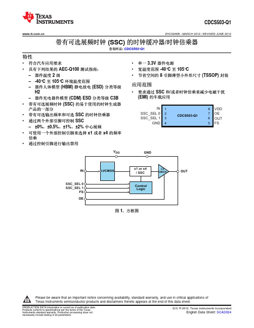
OUTV SSC_SEL SSC_SEL INSSC_SEL 0SSC_SEL 1GNDVDD OE OUT FSCDCS503-Q1ZHCS946B –MARCH 2012–REVISED JUNE 2012带有可选展频时钟(SSC)的时钟缓冲器/时钟倍乘器查询样品:CDCS503-Q1特性•符合汽车应用要求•单一3.3V 器件电源•具有下列结果的AEC-Q100测试指南:•宽温度范围-40°C 至105°C–器件温度2级•节省空间的8引脚薄型小外形尺寸(TSSOP)封装–-40°C 至105°C 环境温度范围应用范围–器件人体模型(HBM)静电放电(ESD)分类等级•要求通过SSC 和/或者时钟倍乘来减少电磁干扰H2(EMI)的车载应用–器件充电器件模型(CDM)ESD 分类等级C3B •带有可选展频时钟(SSC)的易于使用的时钟生成器产品的一部分•带有可选输出频率和可选SSC 的时钟倍乘器•通过两个外部引脚可控制SSC–±0%,±0.5%,±1%,±2%中心展频•可使用一个外部控制引脚来选择x1或者x4的频率倍乘•通过控制引脚进行输出禁用图1.方框图Please be aware that an important notice concerning availability,standard warranty,and use in critical applications of Texas Instruments semiconductor products and disclaimers thereto appears at the end of this data sheet.CDCS503-Q1ZHCS946B–MARCH2012–REVISED 说明CDCS503-Q1是一款带有可选频率倍乘的可展频、LVCMOS输入时钟缓冲器。
时钟弹簧资料
时钟弹簧
方向盘 Steering Wh
柱轴 Column Shaft
1-2.时钟弹簧旳 种类
开关类型
卡扣类型
滚珠型
把时钟弹簧跟组合开关( Multi Function Body)
组装后, 安装在汽车旳种类
把时钟弹簧跟柱轴(Column Shaft)直接组装旳种类
北京当代 时钟弹簧培训目录
1.时钟弹簧产品使用用途
1)时钟弹簧简介 2)时钟弹簧关联 主要事项 3)时钟弹簧缺陷 判断顺序 4)时钟弹簧整备 资料
2. 售后件原因分析阐明 3. 我司生产时钟弹簧旳品质确保
1-1.时钟弹簧产品 使用用途
▶时钟弹簧是什么?
方向连接器总成 旳 简称 (Steering Rolling Connector Assembly)
2-5. 路试时 注意事项
-.车辆出厂前路试时,必须经过S型路线 ⇒因中立位置不对反转旳会断线,噪音发生旳原因.
-.经过S型路线上,将方向盘向右打死,检验SRC中立位置 ⇒假如中立位置不对,方向盘向右打死时SRC内部断线, 气囊灯常亮.
-.经过S型路线上,将方向盘向左打死,检验SRC中立位置. ⇒假如中立位置不对,方向盘向左打死时SRC内部断线, 气囊灯常亮.
- 车辆出厂前,必须要经过S型道路路试后,才干出厂.
2-6. 拆装车时 注意事项
=>进行拆装车前,先将电池正负极断开后进行SRC拆装,以预防造成气囊误爆。
拆装车前确保先将电池正负极断开后, 拔插气囊模块
2-6. 拆装车时 注意事项
=>假如电池正负极不进行断开直接SRC重装,除造成气囊误爆,还会在系统检测时显示 气囊阻值过大。
-.时钟弹簧拆卸安装工作时, 时钟弹簧中立调整后, 安装在车辆上. (往右侧旋转至不动完毕后,再往左侧旋转 标签显示圈回转后, 定中立) ⇒因中立针脱落反转旳会造成断线、噪音发生旳原因.
时钟基础知识

时钟基础知识时钟是我们日常生活中不可或缺的一部分,它在我们的工作、学习和生活中起着至关重要的作用。
本文将介绍一些关于时钟的基础知识,包括时钟的种类、工作原理以及常见故障的排除方法。
一、时钟的种类1. 机械时钟机械时钟是一种使用机械装置来测量时间的时钟。
它采用机械齿轮以及摆线来驱动指针的运动。
机械时钟通常需要通过手动上弦或者摇摆器来维持正常运行。
2. 石英时钟石英时钟是一种通过石英晶体振荡来测量时间的时钟。
石英晶体具有稳定的振荡频率,因此石英时钟比机械时钟更加准确。
石英时钟通常由电池供电。
3. 原子钟原子钟是一种通过原子或分子的高稳定振荡频率来测量时间的时钟。
原子钟的准确度极高,常用于科学实验和导航系统中。
原子钟通常使用铯或铷等元素进行振荡。
二、时钟的工作原理无论是机械时钟、石英时钟还是原子钟,它们的工作原理都是基于稳定的振荡频率来测量时间。
以下是一个简单的时钟工作原理的示意图:[示意图]时钟通过一个稳定的振荡器来产生固定的脉冲信号,这些脉冲信号被转换成可见的时间单位,比如小时、分钟和秒。
机械时钟通过齿轮传动和摆线来驱动指针的运动;石英时钟通过石英晶体的振动来产生电信号,并通过电子电路将其转化为时间单位;原子钟则通过原子或分子的共振频率来产生极为稳定的时间信号。
三、常见故障排除方法1. 时钟走慢或快如果时钟走得慢或快,首先需要检查电池是否正常工作。
若电池耗尽或电池接触不良,可以更换电池或调整电池接触。
另外,石英时钟的振荡器可能会受到温度变化的影响,可以尝试将时钟放置在稳定的温度环境中。
2. 指针不动或越位如果时钟的指针停止运动或者越位,可能是由于机械部件的故障导致。
这时可以尝试打开时钟的后盖,检查机械部件是否正常,如有需要可以进行清洁和维修。
如果是电子时钟,可能是电子电路出现了故障,可以尝试更换电子元件或者直接送修。
3. 时钟噪音大时钟发出噪音通常是由于机械部件磨损或石英晶体振动不均匀所导致。
对于机械时钟,可以尝试加入适量的润滑剂来减少噪音。
主板时钟电路工作原理

主板时钟电路工作原理一、引言主板时钟电路是计算机系统中的重要组成部分,它负责提供系统时钟信号,为计算机的各个部件提供统一的时序参考。
本文将详细介绍主板时钟电路的工作原理及其相关知识。
二、主板时钟电路的作用主板时钟电路的主要作用是为计算机内部的各个部件提供统一的时序参考信号。
它通过产生稳定的时钟信号,确保计算机内部各个部件的协调工作。
时钟信号的频率和稳定性对计算机系统的性能和稳定性有着重要影响。
三、主板时钟电路的组成主板时钟电路一般由以下几个部分组成:1. 振荡器:振荡器是主板时钟电路的核心部件,它负责产生稳定的时钟信号。
常见的振荡器有晶体振荡器和压控振荡器等。
晶体振荡器具有高稳定性和精确的频率特性,被广泛应用于主板时钟电路。
2. 预分频器:预分频器用于将振荡器输出的高频时钟信号分频为较低的频率,以适应不同部件的工作频率要求。
预分频器一般采用可编程分频器,可以根据需要进行设置。
3. 时钟分配器:时钟分配器将预分频器输出的时钟信号分配给不同的部件,以满足各个部件的时钟需求。
时钟分配器一般采用时钟树结构,可以实现多路时钟选择和分频功能。
4. 时钟缓冲器:时钟缓冲器用于放大和驱动时钟信号,确保时钟信号的质量和稳定性。
时钟缓冲器一般采用高速缓冲器,具有较低的时钟延迟和较高的驱动能力。
四、主板时钟电路的工作原理主板时钟电路的工作原理如下:1. 振荡器产生稳定的时钟信号,通常为晶体振荡器,其频率由晶体的特性决定。
2. 振荡器输出的时钟信号经过预分频器进行分频,得到适合不同部件工作频率要求的时钟信号。
3. 预分频器输出的时钟信号经过时钟分配器进行选择和分配,分配给不同的部件。
4. 时钟信号经过时钟缓冲器进行放大和驱动,确保时钟信号的质量和稳定性。
5. 各个部件根据接收到的时钟信号进行相应的操作和计算。
五、主板时钟电路的注意事项在设计和使用主板时钟电路时,需要注意以下几个方面:1. 振荡器的选取:选择适合的振荡器对主板时钟电路的性能和稳定性至关重要。
- 1、下载文档前请自行甄别文档内容的完整性,平台不提供额外的编辑、内容补充、找答案等附加服务。
- 2、"仅部分预览"的文档,不可在线预览部分如存在完整性等问题,可反馈申请退款(可完整预览的文档不适用该条件!)。
- 3、如文档侵犯您的权益,请联系客服反馈,我们会尽快为您处理(人工客服工作时间:9:00-18:30)。
时钟缓冲器基础知识时钟是所有电子产品的基本构建块今天。
用于在同步数字系统中的每个数据过渡,有一个时钟,用于控制的寄存器中。
大多数系统使用晶体,频率时序发生器(FTGS ),或廉价的陶瓷谐振器来产生精确的时钟同步的系统。
此外,时钟缓冲器被用来创建多个副本,乘,除时钟频率,甚至移动时钟边沿向前或向后的时间。
许多时钟缓冲解决方案已经创造了超过过去几年,以解决当今高速逻辑系统所需的许多挑战。
其中一些挑战包括:高工作频率和输出频率,传播延迟从输入到输出,输出到输出歪斜引脚之间,周期tocycle和长期抖动,扩频,输出驱动强度,I / O电压标准和冗余。
因为钟表是最快的信号系统,通常最重的负载下,特别考虑必须在创建时钟树时发出。
在这一章中,我们列出了非PLL和基于PLL的缓冲区的基本功能,并显示这些设备如何被用来解决高速逻辑设计挑战。
在当今的典型的同步设计中,通常需要多个时钟信号,以驱动各种组件。
创建副本的所需数目的时钟树的构建。
树开始于一个时钟源,例如振荡器或外部信号并驱动一个或多个缓冲器。
缓冲器的数量通常是依赖于目标设备的数目和位置。
在过去几年里,通用逻辑组件被用来作为时钟缓冲器。
这些是足够的时间,但他们做一点维持时钟的信号完整性。
事实上,它们实际上是一个不利的电路。
随着时钟树中的速度和时序容限降低增加,传播延迟和输出歪斜变得越来越重要。
在接下来的几节中,我们讨论了旧设备,为什么他们却不足以应付当今的设计需求。
与现代缓冲区相关的常见术语的定义如下。
最后,我们解决了现代时钟缓冲器的属性具有和不具有PLL。
经常被用作时钟源的FTG是一种特殊类型的PLL时钟缓冲器。
◆早期的缓冲器一种时钟缓冲器是一种装置,其输出波形随输入波形。
输入信号传播通过该设备并重新驱动输出缓冲器。
因此,这种装置具有与它们相关联的传播延迟。
此外,由于通过每个输入输出路径上的设备的传播延迟之间的差异,将歪斜的输出之间存在。
一类非PLL时钟缓冲器的一个例子是74F244 ,可从几个制造商。
这些设备已经面世多年,是适用于设计中的频率分别为20MHz以下。
设计师时钟和风扇出来,只会令到在电路卡上的多个同步设备。
有了这些缓慢的频率和相关的上升时间,设计师们适当的利润,用以满足建立和保持时间的同步接口。
然而,这些缓冲区是不是最佳的为今天的高速时钟要求。
该74F244患有长传播延迟(3 〜5 ns)和长输出到输出偏斜延迟。
基于非PLL时钟缓冲器在最近几年有所改善,并使用更先进的I / O设计技术来提高输出至输出偏斜。
随着时钟周期越短,在时钟分配系统的不确定性或歪斜变得更加的一个因素。
由于时钟用于驱动处理器和同步系统部件之间的数据传输,时钟分配系统是系统设计的一个重要组成部分。
时钟分配系统的设计,不采取歪斜考虑可能会导致系统性能下降和可靠性。
◆时钟偏差歪斜是在指定发生在同一时间的两个信号的到达时间的变化。
歪斜是由驱动装置和变异引起的电路板走线布局变化的电路板延时器的输出歪斜。
由于时钟信号驱动系统的许多部件,并且因为所有这些组件应该正好在同一时间,以进行同步接收的时钟信号,在时钟信号的其目的地的到达的任何变化将直接影响系统的性能。
歪斜通过改变时钟边沿的到来将直接影响系统的利润。
因为在同步系统中的元素所需要的时钟信号,以在同一时间到达时,时钟偏差减小其内的信息,可以通过从一个装置到下一个循环时间。
随着系统速度的提高,时钟偏差的总周期时间的比例越来越大。
当循环次数分别为50纳秒,时钟歪斜很少是设计重点。
即使是歪斜的周期时间20 %,它不会引起任何问题。
作为循环次数下降到15ns少,时钟偏差,需要不断增加的设计资源的量。
现在,通常情况下,这些高速系统中只能有10 %专门用于时钟偏移的时序预算的,所以很明显,它必须减少。
有两种类型的时钟偏差的影响系统性能。
时钟驱动器会导致固有偏差和所述印刷电路板(PCB)的布局和设计被称为外源性歪斜。
外在歪斜和布局程序时钟树将在本书后面讨论。
的时间,由于歪斜的变化被定义为以下等式:tSKEW_INTRINSIC =设备引起的偏移tSKEW_EXTRINSIC = PCB +布局+工作环境诱导斜t偏斜= tSKEW_INTRINSIC + tSKEW_EXTRINSIC固有的时钟偏差是造成其本身的时钟驱动器或缓冲器偏移的量。
电路板布局或任何其他设计问题,除了表示对时钟驱动器数据表中的规格不引起内在的歪斜。
◆输出偏斜输出偏斜(TSK )也称为引脚到引脚歪斜。
输出偏移是在相同的转换相同的设备上的任何两个输出端的延迟之间的差异。
联合电子设备工程委员会(JEDEC )的输出歪斜定义为与连接在一起的所有驾驶输入和输出的开关在同一方向驾驶时相同的指定负载一台设备的指定输出之间的偏差。
图2.2和2.3显示一个时钟缓冲器与普通输入,通过Co1_n CIN驾驶输出Co1_1 。
输出的上升沿之间的最大绝对差值将被指定为输出歪斜。
在今天的高性能时钟缓冲器典型的输出歪斜大约是200皮秒(ps)的。
◆输入阈值的变化之后,低偏移时钟信号已分发,时钟接收器必须接受时钟输入以最小的变化。
如果接收机的输入端阈值电平是不均匀的,该时钟接收器将响应于时钟信号在不同的时间产生的时钟偏差。
如果一个负载装置有一个1.2伏的阈值和另一个负载装置具有1.7伏的阈值和上升沿速率为1V/ns的,将会有500 ps的歪斜所引起的在该基础上,负载装置的开关点输入信号。
大多数制造商为中心的设备的输入阈值电平接近1.5伏的标称(TTL )输入设备。
该输入阈值会略有不同,从生产厂家尤其是条件(如电压和温度)的变化。
将TTL规格的输入阈值电平是保证逻辑高时,输入电压高于2.0伏和逻辑低时,输入电压电平低于0.8伏。
这使得一个1.2伏的窗口过电压和温度。
用互补金属氧化物半导体(CMOS)元件轨道摆动的输入有VCC / 2或大约2.5伏,这是比TTL电平高得多的一个典型的输入阈值。
如果阈值电平是不均匀的,时钟偏移会因为这些变化的部件之间发展。
还有很多已经出现,并提供时钟,以不同的子系统时,都必须考虑I / O标准。
表2.1列出下面列出的更普遍的标准随着输入阈值电压。
◆非PLL的时钟驱动器有现代时钟驱动器架构的两种主要类型:缓冲型器件(非PLL)和一个反馈型器件(PLL)。
在缓冲式(非PLL)时钟驱动时,输入波传播通过该装置,并“重新驱动”通过输出缓冲器。
此输出信号直接地跟随输入信号,并具有传播延迟(TPD),取值范围是5纳秒到15纳秒。
这些设备从缓冲器以往不同,如在它们是专为时钟信号而设计的74F244 。
在74F244 ,有八个输入和8路输出。
要创建一个到八个缓冲区,所有八个输入连接在一起。
这会导致过量的负荷在对驱动信号的输入。
一到八个时钟缓冲器只有一个输入,因此只有一个负载。
输出上升和下降时间也难分伯仲,因此不利于占空比误差。
他们改进的I / O结构,引脚到引脚歪斜保持在最低限度。
该设备的输出歪斜,如果它不是数据表上列出的,可以通过减去从最大传播延迟最小传播延迟来计算。
在图2.5所示的10纳秒的tPD时钟驱动器的延迟不考虑影响的电路板布局和设计。
这些类型的设备是极好的缓冲源信号,例如振荡器,其输出相位并不需要匹配输入。
各种各样的基于非PLL缓冲器可在当今市场上,通常范围从少到4路输出,多则30 。
有些设备还包括可配置的I / O和内部寄存器来划分的输出频率。
中最高性能的非今天的PLL基于低电压CMOS (LVCMOS )时钟缓冲器可为B9940L 。
该B9940L是有能力的低电压时钟分配缓冲区选择的差动LVPECL或LVCMOS / LVTTL的兼容的输入时钟。
这两个时钟源可以用于提供一个测试时钟以及初级系统时钟。
所有其他控制输入的LVCMOS / LVTTL的兼容。
十八输出2.5V - 3.3V或兼容,可驱动两个串联端接50欧姆传输线。
有了这个功能,B9940L有一个有效的扇出1:36 。
150 ps的,一个设备的750 PS装置倾斜,以及200MHz的高端工作频率低输出至输出歪曲,使B9940L嵌套时钟树中同步系统的理想时钟分配缓冲区。
这些设备仍然面临设备传播延迟的问题。
通过这些设备的传播延迟是大约5纳秒。
这个延迟会引起歪斜的系统中两个参考时钟的缓冲液和缓冲液的输出需要被对齐。
这些器件还具有输出波形是直接根据输入波形的缺点。
如果输入波形是一个非50 %占空比的时钟,输出波形也将有一个低于理想的占空比。
都在使用这种类型的缓冲区中,需要近50/50输出系统所需的昂贵的晶体振荡器具有严格的公差。
这些器件还缺少逐步调整或频率乘以它们的输出能力。
相位调整允许时钟驱动器,以补偿跟踪传播延迟失配和建立和保持时间的差异,和倍频允许的高频和低频时钟从相同的共同的参考分布。
昂贵的组件和费时的电路板布线技术必须被用来补偿这些缓冲式时钟驱动器设备的功能性缺点。
基于PLL的器件已被纳入到解决所有的这些缺点。
◆零延迟缓冲器零延迟缓冲器(ZDB )是可以扇出的一个时钟信号为多个时钟信号与输出之间的零延迟和非常低歪斜的装置。
该器件非常适合各种要求严格的输入输出时钟分配的应用程序和出倾斜。
一个ZDB的简化框图如图2.7所示。
一个ZDB是建立与使用参考输入和反馈输入一个PLL 。
反馈输入由输出中的一个驱动。
鉴相器调整VCO的输出频率,使得它的两个输入都没有相位或频率的差异。
由于PLL控制回路包括输出和负载中的一个,它会动态地补偿负载放置在该输出。
这意味着,它必须从输入零延迟,驱动该输出负载的反馈独立的输出。
注意,这仅是为了通过反馈输入和所有其它输出被监视的输出有一个输入到输出的延迟是受输出负载的差异的情况。
请参见“超前或滞后调节”这一主题的讨论。
赛普拉斯半导体公司CY2308是一款双银行,通用ZDB提供8个拷贝的单一输入时钟的零延迟从输入到输出和低偏移输出之间。
这种流行的缓冲区是专为在各种时钟分配应用中使用,在本书中,是典型的零延迟,基于PLL的缓冲区将被使用。
外部连接装置上的反馈路径中的能力提供了偏斜控制和开辟了一些有趣的应用程序的机会。
◆使用外部反馈许多ZDBS有一个是简单地通过驱动任何输出到FB引脚为ZDB操作关闭一个开放的外部反馈路径。
然而,在反馈路径可以用于其它有趣的应用。
使用在反馈路径中的离散的延迟元件会产生导致的输入信号的输出。
有时,设计需要一个时钟,是比较早期的输入时钟的剩余份数的一些副本。
图2.9显示了一个电路实现,生成使用ZDB这种早期的时钟。