CT4502型军用多芯组陶瓷电容器pdf
中图分类号查询-TM电工技术

TM 电工技术 [TM-9] 电工技术经济 TM0 一般性问题 TM02 电工设计、制图 TM05 电工安装技术 TM07 电工保养、维修 TM08 电工安全 TM1 电工基础理论 TM11 电工单位、电工计算 [TM12] 电学、磁学 TM13 电路理论 TM131 线性电路 {TM131.1} 电路拓扑学 TM131.2 过渡过程、暂态过程 TM131.3 直流电路 TM131.4 交流电路 TM131.4+1 谐振电路、耦合电路 TM131.4+2 圆图及反演 TM131.4+3 多相电路 TM131.4+4 对称分量 TM131.4+6 多端网络 [TM131.5] 逻辑电路 TM131.6 时变电路 TM132 非线性电路、铁心电路 TM133 电路综合与分析 TM134 分布参数电路 TM135 电路参数 TM14 磁路 TM141 磁导 TM142 直流磁路 TM143 交流磁路 TM144 永久 盘怕? TM15 电磁场理论的应用 TM151 静电场计算方法 TM151+.1 二度场计算 TM151+.2 三度场计算 TM151+.3 电容及部分电容 TM152 电流场、电流场计算 TM153 磁场、磁场计算 TM153+.1 磁场计算 TM153+.2 电感计算 TM153+.3 电磁力 [TM153+.4] 地磁 TM153+.5 磁屏蔽 TM154 交变电磁场 TM154.1 交变电磁场计算 TM154.2 导电体中电磁过程及其应用 TM154.2+1 涡流计算及感应加热 TM154.2+2 集肤作用及邻近作用 TM154.2+3 脉冲磁化 TM154.3 介质和真空中电磁过程及其应用 TM154.4 电磁场逆问题 TM155 场的造型及模拟技术 TM2 电工材料 TM20 一般性问题 TM201 理论 TM201.3 材料分析和计算 TM201.4 材料性能 TM201.4+1 机械性能 TM201.4+2 热性能 TM201.4+3 光性能 TM201.4+4 电性能 TM201.4+5 磁性能 TM201.4+6 表面性能、缺陷 TM202 设计、制图 TM203 结构 TM205 制造工艺及设备 TM2备 TM206 性能试验和测量 TM207 材 细 与防护 TM21/28 各种电工材料 TM21 绝缘材料、电介质及其制品 TM211 有机绝缘材料(总论) TM212 无机绝缘材料(总论) TM213 气体电介质 TM214 液体电介质 TM214+.1 有机酯的液体介质 TM214+.2 合成酯的液体介质 TM215 固体电介质 TM215.1 树脂及塑料、高分子绝缘材料 TM215.1+1 天然树脂 TM215.1+2 合成树脂和塑料 TM215.1+3 改性树脂和塑料 TM215.2 橡胶 TM215.3 绝缘薄膜 TM215.4 绝缘漆(油)、胶合剂 TM215.4+1 掌? TM215.4+2 覆盖漆 TM215.4+3 胶合剂、胶着剂 TM215.5 云母绝缘材料及其制品 TM215.6 纤维绝缘材料及其制品 TM215.7 玻璃绝缘材料 TM215.71 玻璃布 TM215.72 玻璃塑料(有机玻璃) TM215.73 A 纤维 TM215.8 绝缘石料 TM215.91 蜡状绝缘材料 TM215.91+1 非极性蜡、石蜡 TM215.91+2 弱极性蜡、蜂蜡 TM215.92 复合绝缘材料 TM216 绝缘子和套管 TM216+.1 陶瓷绝缘子 TM216+.2 高铝氧瓷绝缘子 TM216+.3 塑料绝缘子、环氧树脂绝缘子 TM216+.4 玻璃绝缘子 TM216+.5 套管 TM216+.51 密封式套管 TM216+.52 穿墙套管 TM216+.53 电器瓷管 TM22 强性介质和压电介质 TM22+1 铁电体、铁电晶体 TM22+2 硫酸盐铁电体 TM22+3 钛酸盐铁电体 TM22+4 钽酸盐铁电体 TM22+5 铌酸盐 TM22+6 锡酸盐 TM22+7 筛格涅特盐 TM22+8 铁磁体 TM22+9.1 石英晶体 [TM23] 半导体材料 TM24 导电材料及其制品 TM241 金属导电材料 TM241.1 精密电阻材料 TM241.2 电热电阻材料 TM242 非金属导电材料、炭素材料 TM243 导电塑料 TM244 裸电线 TM244+.1 圆单线 TM244+.2 架空绞线 TM244+.3 型线与型材 TM244+.4 软接线 TM244+.9 其他 TM245 电磁线、绝缘导线 TM245+.1 漆包线 TM245+.2 纤维绕包电磁线 TM245+.3 无机绝缘电磁线 TM245+.4 耐高温漆包线 TM245+.5 特种电磁线 TM246 电气装备用电线电缆
含宇航级的多芯组瓷介固定电容器标准分析
Ke r s:mut ee n s ea cc p ctr ;n t n lmi tr tn ad;s a elv l y wo d li lme t;c r mi a a i s ai a l a sa d - o o iy r p c e e
1 引言
多 芯组 瓷介 电容 器是 在 片式瓷 介 电容器 的基础 上研 发 的新产 品 。片式 瓷 介 电容器 是 当前 电子无 源
只样 品失 效 ,否则 试 验必 须 进 行 到 2 4h 以上 对 6 。
DI ANZICHANPI KEK N AOXI NG HU YU ANJNG SHI AN I Y
数 为 :6 + .允 许 不合 格数 为 :1 。从 而可 以看 61 只
出 ,S级产 品 所要 求 的母体 数更 多 .在 2组检 验 中
( 般 可 靠 )产 晶 的 相 关 试 验 组 另 进 行 了 对 比 分 析 ,论 述 T B6 8 - 0 9中 S级 ( 航 级 )产 品 的 显 著 特 一 U GJ 7 8 2 0 宇 征 。同 时将 G B6 8 -0 9 美 国军 用标 准 MI- R - 97 J 7820 与 L P F 4 4 0进 行 了 比较 。简 述 了 目前 多 芯组 瓷介 固定 电容 器 国 内外 的应 用 情 况 , 以及 国 内的 供 需 情 况 。对 我 国 尽早 建 立 含 宇 航级 多 芯组 瓷 介 固定 电 容器 生产 线 的贯 标 企 业 、
21 .. 2组 ( 观 和机械 检查 ) 2 外 K级 产 品和 S级 产 品在鉴 定检 验 的 2组 中的试
23 逐 批 检 验 . 231 .. A1 组 分
表 2 过 程 检 验 项 目 比较 表
255型双枪锁定版器件说明书
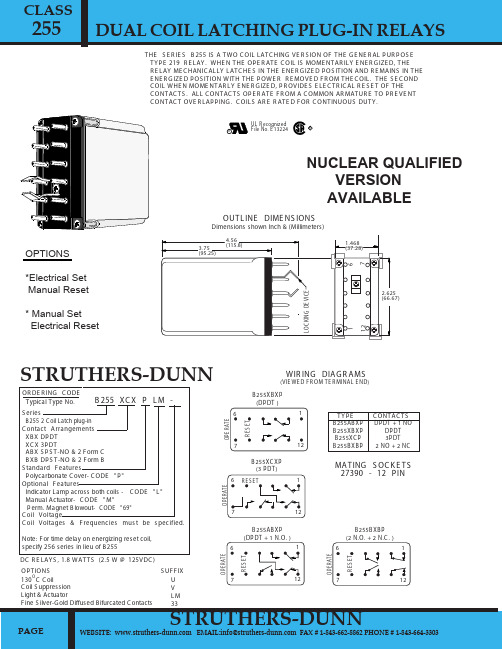
255RUL R ecognized File No. E 13224RTHE S E R IE S B 255 IS A TWO C OIL LATC HING VE R S ION OF THE G E NE R AL P UR P OS E TY P E 219 R E LAY. WHE N THE OP E R ATE C OIL IS MOME NTAR ILY E NE R G IZE D, THE R E LAY ME C HANIC ALLY LATC HE S IN THE E NE R G IZE D P OS ITION AND R E MAINS IN THE E NE R G IZE D P OS ITION WITH THE P OWE R R E MOVE D F R OM THE C OIL. THE S E C OND C OIL WHE N MOME NTAR LY E NE R G IZE D, P R OVIDE S E LE C TR IC AL R E S E T OF THE C ONTAC TS. ALL C ONTAC TS OP E R ATE F R OM A C OMMON AR MATUR E TO P R E VE NT C ONTAC T OVE R LAP P ING. C OILS AR E R ATE D F OR C ONTINUOUS DUTY.U V L M 33S UF F IXOP TIONS130 C C oilC oil S uppression Light & ActuatorF ine S ilver-G old Diffused B ifurcated C ontactsB 255 XC X P L M -S eriesB255 2 C oil Latch plug-in C ontact Arrangements XB X DP DT XC X 3P DTAB X S P S T-NO & 2 F orm C B XB DP S T-NO & 2 F orm B S tandard F eaturesP olycarbonate C over- C ODE "P "Optional F eaturesIndicator Lamp across both coils - C ODE "L " Manual Actuator- C ODE "M" P erm. Magnet B lowout - C ODE "69"C oil VoltageC oil Voltages & F requencies mus t be s pecified.Note: F or time delay on energizing reset coil,specify 256 series in lieu of B 255OR DE R ING C ODE Typical Type No.DC R E LAY S , 1.8 WATTS (2.5 W @ 125VDC )PAGEWEBSITE: EMAIL:info@ FAX # 1-843-662-8862 PHONE # 1-843-664-3303C ONTAC TS61712B 255XB XP (DP DT )61712B 255XC XP (3 P DT)61712B 255AB XP (DP DT + 1 N.O. )R E S E TO P E R A T EO P E R A T ER E S E TR E S E TO P E R A T E61712B 255B XB P (2 N.O. + 2 N.C. )R E S E TO P E R A T EB 255AB XP B 255XB XP B 255XC P B 255B XB PDP DT + 1 NODP DT 3P DT 2 NO + 2 NCWIR ING DIAG R AMS(VIE WE D F R OM TE R MINAL E ND)TY P E4.56(115.8)12167L O C K I N G D E V I C E2.625(66.67)1.468(37.28)3.75(95.25)OUTL INE DIME NS IONSDimensions shown Inch & (Millimeters)MATING S OC K E TS 27390 - 12 P INSTRUTHERS-DUNNSTRUTHERS-DUNN DUAL COIL LATCHING PLUG-IN RELAYSCLASSNUCLEAR QUALIFIED VERSION AVAILABLEOPTIONS*Electrical Set Manual Reset* Manual Set Electrical ResetWE B S ITE : www.s truthers E MAIL:info@ms truthers FAX # 1-843-662-8862 PHONE # 1-843-664-330385% of Nominal Voltage 80 % of Nominal Voltage 110% of nominal, voltageS ilver Alloy & G old Diffused (S tandard)25 mS Max. @ Nominal Voltage.20 mS Max. @ Nominal Voltage.1500 V rms1/4" over surface, 1/8" thru Air-10 C to +60 C10 Million Operations no load100,000 Operations @ R ated Load.500,000 Operations 1/2 R ated Load.C lear polycarbonate.215 g (7.58 oz.) AP P R OX.G E NE R AL S P E C IF IC ATIONSC OIL P ull-in, min. AC P ull-in min. DC Overvoltage, max.C ONTAC TSC ontact Material:TIMINGOperate Time: (operate coil) R elease Time: (R eset coil energized)DIE L E C TR IC S TR E NG THAll Mutually Insulated P oints: Insulation :TE MP E R ATUR E R ated Operation:L IF E E XP E C TANC Y Mechanical: E lectrical:MIS C E L L ANE OUS E nclosure: Weight:RUL R ecognized File No. E 13224R3.014.552.01450500084025615026.54.8 1.104.2015.5540181561224120240R esistance Ohms ± 10%C oil P ower (mA)Nominal Voltage R esistance Ohms ± 10%C oil P ower(mA)80041020045.013.2R E S E T C OIL (3VA)OP E R ATE C OIL (5VA)*AC C OIL , 50/60 HZC OIL S P E C IF IC ATIONS @ 25 C C urrent inrush on all AC coils is less than twice the listedmilliamperes ratings as shown in the AC coil data table.*C urrents shown in table measured at 60 Hz.61224115/125Nominal Voltage DC relays, 1.8 Watts (2.5 W @ 125VDC )DC C OIL DATAR E S E T C OIL 1.4W)38518996.020.015.563.525062002861418014.421.085.03008000R esistance Ohms ± 10%C oil P ower (mA)OP E R ATE C OIL (1.8W)R esistanceOhms± 10%C oil P ower(mA)10A 3A 1A 3A 0.1A0.5A 1.5A 150 mA 0.5A24 VDC 120 VAC 240 VAC 28 VDC 125 VDC125 VDC S M 125 VDC DM 250 VDC S M 250 VDC DMVOLTSMAK E 30A 30A 30A 30A 30A30A 30A 30A 30A10A 10A 10A 10A 10A10A 10A 10A 10A10A 10A 5A 10A 0.5A1.5A 4A 0.5A 1.5AR E S IS TIVE INDUC TIVEC AR R Y B R E AKC ONTAC T R ATING S** F or vers ions with s uffix "69" P ermanent Magnet B lowouts**R elays with C ode 69 feature ( C heck with factory for UL & C S A Listing).PAGESTRUTHERS-DUNN00255DUAL COIL LATCHING PLUG-IN RELAYSCLASS。
陶瓷电容应用

图 3、Y5V 电容的容值温度曲线。
图 4、COG(NPO)电容容值温度曲线
1.2. 电容容量的工作电压稳定性
钽电容容量随电压变化很小。 陶瓷电容中 C0G 类介质的陶瓷电容容量不随电压变化而变化。X7R 和 X5R 类介质的陶瓷 变化稍大,下面图 5 是 AVX 的 X7R 电容容量随外加电压变化的曲线,在额定电压下容量损失 10%左右。据 KEMET 网站介绍,某些 X7R 和 X5R 介质电容在额定电压下容量损失达 40%。 Y5V 介质电容容量随工作电压上升而迅速下降,在 40%额定电压下容量损失即达 80%(AVX), 参见图 6。即介电常数越高,容量损失越厉害。下面的曲线均指室温。 外加交流电压时 X7R 的容量会增加,见下面图 7。同时 DF 值也增加。
1.8. 失效特性
片式钽电容、铝电解电容、陶瓷电容的最常见失效方式均为大漏电流或者短路。失效后器 件、PCB 温度迅速上升,普通型钽电容由于有 MnO2 做氧化剂,失效后会起火,而聚合物型钽 电容、铝电解电容、陶瓷电容则没有这个缺点
片式钽电容和铝电解电容外部均有环氧封装,因此可以承受一定冲击、PCB 应力。陶瓷电 容和简单封装(外部无环氧)的钽电容抗机械冲击、热冲击、应力能力较差,热膨胀系数失配 时也容易失效。
技术积累
陶瓷电容在模块电源中的应用
陶瓷电容在模块电源中的应用
1. 陶瓷电容特性及与其它电容对比
从封装形式来说陶瓷电容有引线和 SMD 型,模块电源中一般为 SMD 型,下面均指 SMD 型。
按介质材料来分,陶瓷电容可分两大类:I 类介质和 II 类介质。I 类介质主要有钛酸盐 构成,但钛酸钡不是主要成分,特点是介电系数低,构成的电容器容量小,但电性能稳定, 没有随时间老化的特性,电容量随温度、电压、频率变化小,绝缘电阻高,损耗小(Q 值 高)。最常见的 I 类介质电容是 COG(NPO)型温度补偿电容(可小于正负 30 ppm/℃)。
KEMET PME264系列金属胶电容器产品说明书

Benefits• Approvals: ENEC, UL, cUL• Rated voltage: 660 VAC 50/60 Hz • Capacitance range: 0.001 – 0.1 µF • Lead spacing: 15.2 – 25.4 mm • Capacitance tolerance: ±20%• Climatic category: 40/85/56, IEC 60068–1• Tape and reel in accordance with IEC 60286–2• RoHS Compliant and lead-free terminationsOverviewThe PME264 Series is constructed of multilayer metallized paper encapsulated and impregnated in self-extinguishing material meeting the requirements of UL 94 V–0.ApplicationsTypical applications include worldwide use inelectromagnetic interference suppression in all X2 and across-the-line applications. These capacitors are also for use in high AC and DC voltage applications such as commutator capacitor in converters and ignition circuits.AC Line EMI Suppression and RC NetworksPME264 Series Metallized Impregnated Paper, Class X2, 660 VACLegacy Part Number SystemNew KEMET Part Number SystemClick image above for interactive 3D contentOpen PDF in Adobe Reader for full functionalityOrdering Options Table Benefits cont'd• Operating temperature range of −40˚C to +85˚C• 100% screening factory test at 3,000 VDC• The highest possible safety regarding active and passive flammability• Excellent self-healing properties ensure long life even when subjected to frequent over-voltages • Good resistance to ionization due to impregnated dielectric • High dV/dt capability• The impregnated paper ensures excellent stability and outstanding reliability properties, especially in applications with continuous operationDimensions – MillimetersFRONT VIEW SIDE VIEWPerformance CharacteristicsEnvironmental Test DataApprovalsEnvironmental ComplianceAll KEMET EMI capacitors are RoHS Compliant.Table 1 – Ratings & Part Number Reference(1) Insert ordering code for lead type and packaging. See Ordering Options Table for available options.Soldering ProcessThe implementation of the RoHS directive has resulted in the selection of SnAgCu (SAC) alloys or SnCu alloys as primary solder. This has increased the liquidus temperature from that of 183ºC for SnPb eutectic alloy to 217 – 221ºC for the new alloys. As a result, the heat stress to the components, even in wave soldering, has increased considerably due to higher pre-heat and wave temperatures. Polypropylene capacitors are especially sensitive to heat (the melting point of polypropylene is 160 – 170ºC). Wave soldering can be destructive, especially for mechanically small polypropylene capacitors (with lead spacing of 5 mm to 15 mm), and great care has to be taken during soldering. The recommended solder profiles from KEMET should be used. Please consult KEMET with any questions. In general, the wave soldering curve from IEC Publication 61760-1 Edition 2 serves as a solid guideline for successful soldering. Please see Figure 1.Reflow soldering is not recommended for through-hole film capacitors. Exposing capacitors to a soldering profile in excess of the above the recommended limits may result to degradation or permanent damage to the capacitors.Do not place the polypropylene capacitor through an adhesive curing oven to cure resin for surface mount components. Insert through-hole parts after the curing of surface mount parts. Consult KEMET to discuss the actual temperature profile in the oven, if through-hole components must pass through the adhesive curing process. A maximum two soldering cycles is recommended. Please allow time for the capacitor surface temperature to return to a normal temperature before the second soldering cycle.Manual Soldering Recommendations Following is the recommendation for manual soldering with a soldering iron.The soldering iron tip temperature should be set at 350°C (+10°C maximum) with the soldering duration not to exceed more than 3 seconds.Recommended Soldering TemperatureSoldering time (sec)S o l d e r i n g i r o n b i t t e m p e r a t u r e (d e g C )0501001502002503004080120160200240T e m p e r a t u r e (°C )Time (s)Soldering Process cont'dWave Soldering Recommendations cont'd1. The table indicates the maximum set-up temperature of the soldering processFigure 12. The maximum temperature measured inside the capacitor:Set the temperature so that inside the element the maximum temperature is below the limit:Temperature monitored inside the capacitor.Selective Soldering RecommendationsSelective dip soldering is a variation of reflow soldering. In this method, the printed circuit board with through-holecomponents to be soldered is preheated and transported over the solder bath as in normal flow soldering without touching the solder. When the board is over the bath, it is stopped and pre-designed solder pots are lifted from the bath with molten solder only at the places of the selected components, and pressed against the lower surface of the board to solder the components.The temperature profile for selective soldering is similar to the double wave flow soldering outlined in this document, however, instead of two baths, there is only one bath with a time from 3 to 10 seconds. In selective soldering, the risk ofoverheating is greater than in double wave flow soldering, and great care must be taken so that the parts are not overheated.ConstructionDetailed Cross SectionSelf-ExtinguishingSelf-ExtinguishingResinMetal ContactLayerMetal ContactLayerMarginMetallized Impregnated Paper(First Layer)MarginMetallized Impregnated Paper(Second Layer)Metal Spraying Impregnated Series Design — Multilayer Impregnated Paper Dielectric2 SectionWinding SchemeMarkingBACKFRONTTOPSeriesSelf HealingPackaging QuantitiesLead Taping & Packaging (IEC 60286–2)Taping Specifi cation(1) Maximum cumulative feed hole error, 1 mm per 20 parts.(2) 16.5 mm available on request.(3) Depending on case size.(4) 15 mm available on request.Lead Taping & Packaging (IEC 60286–2) cont'd Ammo Specifi cationsReel Specifi cationsManufacturing Date Code (IEC–60062)KEMET Electronic Corporation Sales Offi cesFor a complete list of our global sales offi ces, please visit /sales.DisclaimerAll product specifi cations, statements, information and data (collectively, the “Information”) in this datasheet are subject to change. The customer is responsible for checking and verifying the extent to which the Information contained in this publication is applicable to an order at the time the order is placed.All Information given herein is believed to be accurate and reliable, but it is presented without guarantee, warranty, or responsibility of any kind, expressed or implied. Statements of suitability for certain applications are based on KEMET Electronics Corporation’s (“KEMET”) knowledge of typical operating conditions for such applications, but are not intended to constitute – and KEMET specifi cally disclaims – any warranty concerning suitability for a specifi c customer application or use. The Information is intended for use only by customers who have the requisite experience and capability to determine the correct products for their application. Any technical advice inferred from this Information or otherwise provided by KEMET with reference to the use of KEMET’s products is given gratis, and KEMET assumes no obligation or liability for the advice given or results obtained.Although KEMET designs and manufactures its products to the most stringent quality and safety standards, given the current state of the art, isolated component failures may still occur. Accordingly, customer applications which require a high degree of reliability or safety should employ suitable designs or other safeguards (such as installation of protective circuitry or redundancies) in order to ensure that the failure of an electrical component does not result in a risk of personal injury or property damage.Although all product–related warnings, cautions and notes must be observed, the customer should not assume that all safety measures are indicted or that other measures may not be required.KEMET is a registered trademark of KEMET Electronics Corporation.。
SMT技术第三讲

桂林电子科技大学职业技术学院
课前回顾
1、表面组装元器件的分类?
表面组装元件、表面组装器件、表面组装连接件
2、电阻、电位器和排阻的异同?
3、表面组装电阻的分类、电阻制造工艺。
表面组装电容器
表面组装电容器又称片式电容器,主要在调谐电
路、旁路电路、耦合电路和滤波电路中起着重要作用。
片式瓷介电容器因陶瓷配方不同而具有不同电性能:
1)Ⅰ型陶瓷CC41—介电常数<100,稳定性、可靠性高 2)Ⅱ型陶瓷CT41—介电常数>100,稳定性较好 3)Ⅲ型陶瓷—具有很高的介电常数,稳定性差,易损耗
瓷介电容器的特点
A 介质材料为陶瓷,耐热性能好 B 耐酸碱及盐类腐蚀,抗腐蚀性能好 C 低频陶瓷材料介电常数大,体积小、容量大 D 陶瓷绝缘性能好,可制成高压电容器 E 陶瓷材料损耗与频率关系很小,适用于高频 F 陶瓷价格便宜,原料丰富 G 瓷介电容器电容量较小,机械强度较低
滤波—将信号中特定波段频率滤除的操作,是抑制和防止干扰的一项重 要措施。
多层片式瓷介电容器
片式瓷介电容器有矩形和圆柱形两种形式,其中,圆柱
形为单层结构,矩形电容大多为多层叠层结构,又称MLC
(Multilayer Ceramic Capacity)。该类电容器以陶 瓷为介质,涂覆金属薄膜经高温烧结形成电极并焊上引出线, 外表涂保护漆或采用聚合物封装。
片式薄膜电容器
片式微调电容器
片式微调电容器可在某一小范围内调整电容量, 调整后可将电容值固定在某个电容值。类似于可调 电位器,但应用领域很窄。
片式电感器
片式电感器亦称表面贴装电感器,与其它片式
元器件(SMC及SMD)一样,是适用于SMT技术的新一 代无引线或短引线微型电子元件,其引出端的焊接 面在同一平面上。在电路中起扼流、退耦、滤波、 调谐、延迟、补偿等作用。
CCS41、CTS41系列宇航级片式多层瓷介电容器

火炬牌军用电容器选型指南
Application Guideline of Torch Military Capacitors
CCS41系列 CTS41系列宇航级片式多层瓷介电容器
1 执行标准
总 规 范 : GJB4157-2001《高可靠瓷介固定电容器总规范》 详 细 规 范 : ZZR-Q/HJ20001A-2007《CCS41型宇航级无引线
07
火炬牌军用电容器选型指南
Application Guideline of Torch Military Capacitors
CCS41系列 CTS41系列宇航级片式多层瓷介电容器
5 其它参数
特性 BP
损耗角正切 tgδ≤15X10-4
BX
tgδ≤250X10-4
介质耐电压 3.0UR
25℃绝缘电阻 CR≤0.01µF IR≥105 MΩ CR>0.01µF IR ≥1C0R00 MΩ
Tmax
1.20
2.01±0.20 1.25±0.20
1.40
3.20±0.20 1.60±0.20
1.80
3.20±0.20 2.50±0.20
2.70
t 0.50±0.25
0.50±0.25
0.50±0.25
0.50±0.25
※单位:mm ※1210尺寸可覆盖1206尺寸的所有容量范围,条件允许时应优先选用1210,避免使用1206。
CR≤0.01µF IR≥105 MΩ
1000
CR>0.01µF IR ≥ CR MΩ
125℃绝缘电阻
CR≤0.01µF IR≥104 MΩ
CR>0.01µF
IR
≥
100 CR
军用多层瓷介电容器等点及标准规范试验要求
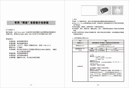
“軍婦 ” 級射頻高Q 多屋片式瓷介屯容器
1.特�
﹒尺寸規格系列化,遁用于混合集成屯路或印刷屯路的表面貼裝元件﹔ ﹒具有高Q值、低ESR、可靠性高的特且是﹔ ﹒損耗低, 屯容量穩定性高、工作頻率最高可迷3GHz﹔ ﹒軍用通訊、雷遠、炮彈引信、艘船及航空、航天、武器系統的地面屯子設各及民用高端設各。 .這用于各美設各中的高頻屯路、VHF_;微波康、射頻及放大血路中﹔
nF GO
“軍婦 ” 級二美 多屋瓷介屯容器
1.特息:
﹒矩形, 尺寸規格系列化, 這用于混合集成屯路或印刷屯路的表面貼裝元件﹔ ﹒具有介屯常數高, 也容器容量体棋比大的特息﹔ ﹒有Ag (Cu) -Ni-Sn多神端也很引出材料, 特別造用于表面組裝技朮封可焊性和耐焊接熱
的戶格要求﹔ ﹒軍用通訊、 雷遠、炮彈引信、艘船及航空、航天、武器系統的地面屯子設各及民用高端
COG:
前兩位數字方 C± : 0.25pF D:±0.50pF
0± 30ppm/'t 有效數字,后 F:±1.0%
-55 't -125℃ 一位數字均10 G: ±2.0%
的軍數﹔
J: ±5.0%
K± : 10%
前兩位數 字均有效 數字, 后 N:三是屯髏 一位數字 Ag( Cu)/Ni/Sn ,i10的軍 數﹔
T:舖帶 包裝﹔ B或空缺: 散包裝
4. 外形尺寸參數 4.1片式屯容器
尺寸 代碼
尺寸( mபைடு நூலகம்)
L
w
Tmax
0 6 0 3 1 . 5 2 ±0.2 5 0.76± 0.2 5 1.0 1
080 5
2.0 0±0.2 5 1.2 5±0.2 5 1.4 5
1 20 6