多层片式瓷介电容器((MLCC)
多层陶瓷电容
多层陶瓷电容一、什么是多层陶瓷电容?多层陶瓷电容(MLCC)是一种常见的电子元件,用于电路中的信号整形、滤波、耦合和终端阻抗匹配等应用。
其基本结构由多层陶瓷薄片和金属电极堆叠而成,其中陶瓷层作为电介质存储能量,金属电极用于连接电路。
多层陶瓷电容具有高容量密度、低电阻、优异的高频性能和稳定性等特点。
二、多层陶瓷电容的分类多层陶瓷电容根据其材料、结构和电容量可以进行分类。
2.1 材料分类•标准陶瓷电容:以镁钛酸钡(BaTiO3)为基础材料,具有较高的介电常数和良好的温度稳定性。
标准陶瓷电容广泛应用于消费电子产品和工业设备中。
•超低温陶瓷电容:添加稀土元素或其他添加剂,可以显著降低介电常数和温度系数,提高电容在低温环境下的稳定性,适用于航天航空等极端环境中的应用。
•超高温陶瓷电容:采用高熔点材料制备,可以在高温环境中保持稳定性,适用于汽车引擎、电源模块等高温环境的电子设备。
2.2 结构分类•X7R结构:具有一定的介电常数、温度系数和电压稳定性,是最常用的结构。
适用于大部分一般性的应用场景。
•X5R结构:与X7R相比,具有更高的介电常数和更大的温度系数。
适用于电容量较大且要求高温环境稳定性的应用。
•X8R结构:具有较低的温度系数和良好的高温稳定性,适用于高温环境的电路设计。
2.3 电容量分类多层陶瓷电容的电容量范围广泛,从几皮法到数百微法不等。
根据具体应用需求,选择合适的电容量是确保电路性能稳定的重要因素。
三、多层陶瓷电容的特性多层陶瓷电容具有以下几个重要的特性:3.1 高容量密度多层陶瓷电容的高容量密度使得在有限的空间内可以存储更多的能量,满足电路的需求,对于体积要求敏感的应用十分重要。
3.2 低电阻多层陶瓷电容具有较低的ESR(Equivalent Series Resistance),使其在高频条件下具有良好的电流响应能力。
这使得它适用于需要高频稳定性和低噪声的电路设计。
3.3 高频性能多层陶瓷电容具有优异的高频性能,可以在高频条件下保持稳定的电容值和低损耗。
什么是多层片式瓷介电容器((MLCC)

什么是多层片式瓷介电容器((MLCC)
多层瓷介电容器(MLCC)---简称片式电容器,是由印好电极(内电极)的陶
瓷介质膜片以错位的方式叠合起来,经过一次性高温烧结形成陶瓷芯片,再在
芯片的两端封上金属层(外电极),从而形成一个类似独石的结构体,故也叫
独石电容器。
片式电容器除有电容器“隔直通交”的通性特点外,其还有体积小,比容大,寿命长,可靠性高,适合表面安装等特点。
•随着世界电子行业的飞速发展,作为电子行业的基础元件,片式电容器也以惊人的速度向前发展,•
每年以10%~15%的速度递增。
目前,世界片式电容的需求量在2000 亿支以上,70%出自日本,其次是欧美和东南亚(含中国)。
随着片容产品可靠性和集成度的提高,其使用的范围越来越广,•广泛地应用于各种军民用电子整机和电子设备。
如电脑、电话、程控交换机、精密的测试仪器、雷达通信等。
片式电容器的基本结构简单的平行板电容器的基本结构是由一个绝缘的中间
介质层加外两个导电的金属电极,基本结构如下:
因此,多层片式陶瓷电容器的结构主要包括三大部分:陶瓷介质,金属内电极,金属外电极。
而多层片式陶瓷电容器它是一个多层叠合的结构,简单地说
它是由多个简单平行板电容器的并联体。
图3-实物结构图
片式电容的发展趋势
为了满足电子整机不断向小型化、大容量化、•高可靠性和低成本的方向发展。
多层片式电容器也随之迅速向前发展:种类不断增加,•体积不断缩小,性能不断提高,技术不断进步,材料不断更新,•轻薄短小系列产品已趋向于。
MLCC片式多层陶瓷电容器工艺技术(doc 35页)

C = εr×ε0×A×n / T
The rated voltage depends on the structure of the device, the thickness and strength of the dielectric Figure 1 shows the structure of a multi-layer capacitor.
General Introduction Multi-layer ceramic chip capacitor is a kind of ceramic dielectric capacitor with small size, high capacitance per volume, high accuracy, suited surface mounted technology (SMT). It is widely used in electronic circuitry, mounted printed circuit board, and hybrid IC. These different functions require specific capacitor properties.
MLCC 片式多层陶瓷电容器工艺 技术(doc 35 页)
简介 Brief Introduction
▉ MLCC 简介: 片式多层陶瓷电容器(MLCC)是适合于表面贴装技术(SMT)的小尺寸、
MLCC老化特性
片式多层陶瓷电容器(MLCC)老化特性高介电常数型陶瓷电容器 (标准的主要材料为BaTiO3,温度特性为X5R,X7R,Y5V等) 的电容量随时间而减小。
这一特性称之为电容老化。
电容老化是具有自发性极化现象的铁电陶瓷独有的现象。
当陶瓷电容器加热到居里点以上的温度时 (在该温度晶体结构发生改变,自发性极化消失 (大约为150°C) ),并使之处于无载荷状态,直到它冷却到居里点以下,随着时间的流逝,逆转自发性极化变得越来越困难,结果,所测的电容值会随着时间而减小。
上述现象不仅在三星的产品中,在所有高介电常数 (BaTiO3) 的一般性陶瓷电容器都可以观察到。
附录是一些有关电容老化的公用标准 (陶瓷电容器:IEC60384-22附录B等)。
当电容值由于老化而不断减小的电容器重新加热到居里点以上温度并让其冷却时,电容值会得到恢复。
这种现象称之为去老化现象,发生去老化后,正常的老化过程重新开始。
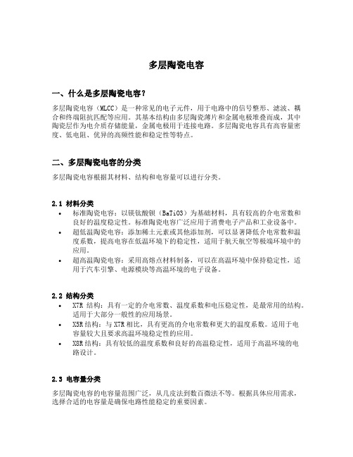
质陶瓷的自发极化与铁电现象BaTiO3质陶瓷的自发极化与铁电现象如图1所示,BaTiO3质陶瓷具有钙钛矿晶体结构。
在居里点 (约130°C) 温度以上呈立方体,且钡 (Ba) 的位置位于最高点,氧 (O)位于晶面的中心,钛 (Ti) 位于晶体的中心。
图1: BaTiO3质陶瓷的晶体结构当在居里点以下正常温度范围内,一条晶轴 (C轴) 伸长约1%而其他晶轴缩短,晶体变成四方晶格 (如下页图2所示)。
在这种情况下,Ti4+离子将占据附近O2-的位置而后者从晶体中心沿晶轴伸展的方向偏移0.12Å。
这种偏移导致正、负电荷的生点发生偏差,造成极化现象。
极化现象是由于晶体结构的不对称造成的,在不施加外电场或压力的情况下,这种极化现象从一开始就存在。
这种类型的极化称为自发性极化现象。
图2: 温度变化时的晶体结构和相关介电常数的变化 (纯BaTiO3)BaTiO3质陶瓷自发极化的方向 (Ti4+离子的位置) 在施加外部电场的情况下可以轻易逆转。
片式多层陶瓷电容器简介介绍

应用领域
通信设备
用于信号处理、滤波、去耦等电路中,提高 信号质量。
汽车电子
用于汽车发动机控制、安全气囊等汽车电子 系统中。
消费电子
广泛用于智能手机、平板电脑、数码相机等 电子产品中。
工业控制
用于工业自动化设备、电机驱动控制等电路 中。
02
片式多层陶瓷电容器的制造工 艺
片式多层陶瓷电容器的制造工艺
智能化与自动化
随着智能化和自动化技术的不断 发展,片式多层陶瓷电容器的生 产工艺也在不断改进,提高生产 效率和产品质量。
技术挑战与解决方案
技术挑战
片式多层陶瓷电容器的技术挑战主要 包括提高性能、减小体积、降低成本 等方面。
解决方案
针对这些挑战,企业可以通过研发新 材料、优化生产工艺、提高生产效率 等方式来应对。同时,加强与高校、 科研机构的合作也是解决技术难题的 重要途径。
它利用陶瓷介质的高介电常数特性,实现小型化、高容量的电容器。
特性
高容值
由于采用多层叠加结构,片式 多层陶瓷电容器的容值较高。
小型化
体积小巧,有利于电子设备的 小型化和集成化。
高频特性好
具有较低的等效串联电阻(ESR )和等效串联电感(ESL),适 用于高频电路。
可靠性高
经过严格的质量控制和可靠性 测试,具有较长的使用寿命。
• 片式多层陶瓷电容器(MLCC)是一种电子元件,广泛应用于各类电子设备中,具有小型化、高性能、高可靠性的特点。 MLCC由多层陶瓷介质和金属电极叠合而成,具有高介电常数、低损耗、温度稳定性好等优点。
03
片式多层陶瓷电容器的性能参 数
片式多层陶瓷电容器的性能参数
• 片式多层陶瓷电容器(MLCC)是一种电子元件,广泛应 用于各类电子设备中,作为微型、高精度、高可靠性的电 容元件。它由多层陶瓷介质和金属电极叠加而成,具有体 积小、容量大、成本低、一致性好等优点。
mlcc(片层陶瓷电容)

mlcc(片层陶瓷电容)下载温馨提示:该文档是我店铺精心编制而成,希望大家下载以后,能够帮助大家解决实际的问题。
文档下载后可定制随意修改,请根据实际需要进行相应的调整和使用,谢谢!并且,本店铺为大家提供各种各样类型的实用资料,如教育随笔、日记赏析、句子摘抄、古诗大全、经典美文、话题作文、工作总结、词语解析、文案摘录、其他资料等等,如想了解不同资料格式和写法,敬请关注!Download tips: This document is carefully compiled by the editor. I hope that after you download them, they can help yousolve practical problems. The document can be customized and modified after downloading, please adjust and use it according to actual needs, thank you!In addition, our shop provides you with various types of practical materials, such as educational essays, diary appreciation, sentence excerpts, ancient poems, classic articles, topic composition, work summary, word parsing, copy excerpts,other materials and so on, want to know different data formats and writing methods, please pay attention!在现代电子设备中,mlcc(片层陶瓷电容)扮演着至关重要的角色。
MLCC—搜狗百科

MLCC—搜狗百科 MLCC是⽚式多层陶瓷电容器英⽂缩写.(Multi-layer ceramic capacitors)⼀、瓷介的分类 陶瓷电容⼀般是以其温度系数作为主要分类。
Class I - ⼀类陶瓷(超稳定)EIA称之为COG 或NPO。
⼯作温度范围 -55℃~+125℃,容量变化不超过±30ppm/℃。
电容温度变化时,容值很稳定,被称作具有温度补偿功能,适⽤于要求容值在温度变化范围内稳定和⾼Q值的线路以及各种谐振线路。
Class II/III - ⼆/三类陶瓷(稳定)EIA标称的X7R表⽰温度下限为-55℃;上限温度为+125℃的⼯作温度范围内,容量最⼤的变化为 ±15%,Z5U、Y5V分别表⽰⼯作温度10~+85℃和-30~+85℃;容量最⼤变化为+22~-56%和30~82%,同属于⼆类陶瓷。
优点是体积利⽤率⾼,即在外型尺⼨相同时能提供更⾼的容值,适⽤于⾼容值和稳定性能要求不太⾼的线路。
⼆、瓷介代号陶瓷介质的代号是按其陶瓷材料的温度特性来命名的。
⽬前国际上通⽤美国EIA标准的叫法,⽤字母来表⽰。
常⽤的⼏种陶瓷材料的含义如下:Y5V:温度特性Y代表-25℃; 5代表+85℃;温度系数V代表-80%~+30%Z5U:温度特性Z代表+10℃; 5代表+85℃;温度系数U代表-56%~+22%X7R:温度特性X代表-55℃; 7代表+125℃温度系数R代表 ± 15%NP0:温度系数是30ppm/℃(-55℃~+125℃)三、⼀般电性能1、介电常数不同介质的类别有不同的表现效果。
环境因素,包括温度、电压、频率和时间(⽼化),对不同介质的电容有不同的影响。
介质常数(K值)越⾼,稳定性能、可靠性能和耐⽤性能便越差。
现代多层陶瓷电容器介质最常⽤有以下三类。
· COG或NPO(超稳定) K值10~100· X7R(稳定)K值2000~4000· Y5V或Z5U(⼀般⽤途)K值5000~250002、绝缘电阻(IR)即介质直流电阻,通常测量⽅法是以额定电压将电容充电⼀分钟,电容充电以后测量其漏电电流。
多层陶瓷片电容器说明书
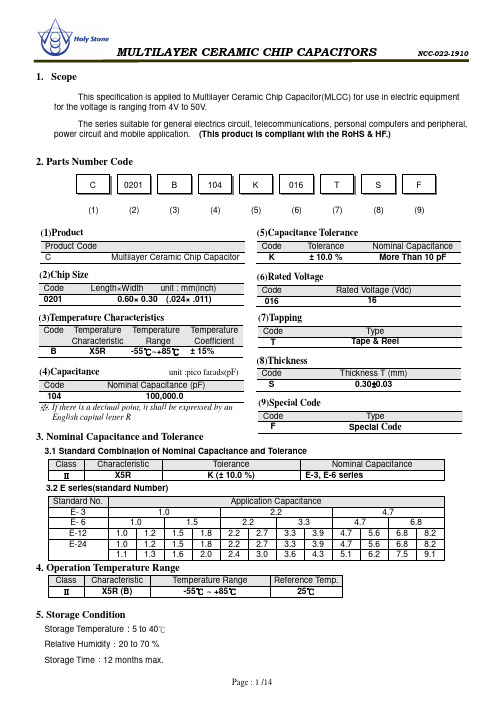
1. ScopeThis specification is applied to Multilayer Ceramic Chip Capacitor(MLCC) for use in electric equipment for the voltage is ranging from 4V to 50V.The series suitable for general electrics circuit, telecommunications, personal computers and peripheral, power circuit and mobile application. (This product is compliant with the RoHS & HF.)2. Parts Number Code3. Nominal Capacitance and Tolerance3.1 Standard Combination of Nominal Capacitance and ToleranceClass CharacteristicTolerance Nominal CapacitanceⅡX5RK (± 10.0 %)E-3, E-6 series3.2 E series(standard Number) Standard No.Application CapacitanceE- 3 1.02.24.7E- 6 1.0 1.52.23.34.76.8E-12 1.0 1.2 1.5 1.8 2.2 2.7 3.3 3.9 4.7 5.6 6.8 8.2 E-241.0 1.2 1.5 1.82.2 2.73.3 3.94.75.66.8 8.2 1.1 1.31.62.02.43.0 3.64.35.16.27.5 9.14. Operation Temperature RangeClassCharacteristic Temperature Range Reference Temp.Ⅱ X5R (B)-55 ~ +85℃℃25℃5. Storage ConditionStorage Temperature :5 to 40℃ Relative Humidity :20 to 70 % (1) (2) (3) (4) (5)(6)(7)(6)Rated VoltageCode Rated Voltage (Vdc)01616(1)ProductProduct Code C Multilayer Ceramic Chip Capacitor (3)Temperature CharacteristicsCode Temperature CharacteristicTemperature Range TemperatureCoefficientB X5R -55℃~+85℃ ± 15%(4)Capacitance unit :pico farads(pF) Code Nominal Capacitance (pF) 104 100,000.0※. If there is a decimal point, it shall be expressed by an English capital letter R(5)Capacitance ToleranceCode Tolerance Nominal Capacitance K± 10.0 %More Than 10 pF(7)TappingCode Type TTape & Reel(2)Chip Size Code Length×Width unit : mm(inch)02010.60× 0.30 (.024× .011)(8)(9)(8)ThicknessCode Thickness T (mm)S0.30±0.03(9)Special CodeCode TypeFSpecial Code6. Dimensions6.1 Configuration and Dimension :Unit:mmTYPE LW TB (min)BW (min) 02010.60± 0.030.30± 0.030.30± 0.030.200.106.2 Termination Type :External Electrodes BarrierInner ElectrodesPolymer Electrodes (If applicable)7. PerformanceFig.1P.C. Board for Bending Strength TestMaterial : Glass Epoxy Substrate: Solder ResistTest SubstrateMaterial : Glass Epoxy Substrate: Copper (Thickness : 0.035mm)Thickness : 1.6 mmUnit:mmType A B C 0201 0.2 0.9 0.4 0402 0.5 1.5 0.6 0603 1.0 3.0 1.0 0805 1.2 4.0 1.6 1206 2.2 5.0 2.0 1210 2.2 5.0 2.9 1808 3.5 7.0 2.5 1812 3.5 7.0 3.7 2208 4.5 8.0 2.5 2211 4.5 8.0 3.0 22204.58.05.68. Packing8.1 Bulk PackingAccording to customer request. 8.2 Chip Capacitors Tape Packing8.3 Material And QuantityTape Material 0201 0402 0603/0805 ≦T 0.33mm ≦T 0.55mm ≦T 1.00mm T >1.00mm Paper 15,000 pcs/Reel 10,000 pcs/Reel 4,000 pcs/Reel NAPlasticNA NA NA 3,000 pcs/ReelTape Material 1206≦T 1.00mm 1.00mm <≦T 1.25mmT >1.25mmPaper 4,000 pcs/ReelNANAPlastic NA3,000 pcs/Reel 2,000 pcs/ReelTape Material 1812/2211/2220 1825/2225 2208 T ≦2.20mm T >2.20mm T ≦2.20mm T >2.20mm T ≦2.20mm Paper NA NA NA NANAPlastic 1,000 pcs/Reel 700 pcs/Reel 700 pcs/Reel400 pcs/Reel 1,000 pcs/Reel NA :Not Available8.4 Cover Tape Reel Off Force8.4.1 Peel-Off Force5 g·≦f Peel-≦Off Force 70 g·f 8.4.2 Measure MethodTape Material 1808/1210≦T 1.25mm1.25mm <≦T2.40mmT >2.40mmPaper NANANAPlastic 3,000 pcs/Reel1,000/2,000 pcs/Reel500/1,000 pcs/Reel8.5 Paper TapeUnit:mm8.6 Plastic TapeUnit:mm TYPE A B C DE 0201 0.37± 0.1 0.67± 0.1 4.00± 0.1 2.00± 0.052.00± 0.10402 0.61± 0.1 1.20± 0.1 0603 1.10± 0.2 1.90± 0.2 4.00± 0.10805 1.50± 0.2 2.30± 0.2 1206 1.90± 0.2 3.50± 0.2 1210 2.90± 0.2 3.60± 0.2 TYPE FG H It0201 1.75± 0.103.50± 0.058.0± 0.30 φ1.50 +0.10/-0 1.10 max.0402 0603 0805 1206 1210Type A B C D E F 0805 1.5±0.2 2.3±0.2 4.0± 0.12.0± 0.054.0± 0.11.75± 0.11206 1.9±0.2 3.5±0.2 1210 2.9±0.2 3.6±0.2 1808 2.5±0.2 4.9±0.2 1812 3.6±0.2 4.9±0.2 8.0± 0.11825 6.9±0.2 4.9±0.2 2208 2.5±0.2 6.1±0.2 2211 3.2±0.2 6.1±0.2 2220 5.4±0.2 6.1±0.2 22256.9±0.26.1±0.28.7 Reel DimensionsReel Material :PolystyreneType G H IJ t O 0805 3.5± 0.058.0± 0.3φ1.5+0.1/-03.0 max.0.3 max.1.0± 0.11206 1210 1808 5.5± 0.05 12.0 ± 0.3 4.0 max. 1.5± 0.11812 1825 2208 2211 2220 2225Type AB C DE W 0201 φ382 max φ50 min φ13± 0.5φ21± 0.82.0±0.510± 0.150402 0603 0805 1206 1210 1808 φ178±2.0 φ60±2.0 13±0.31812 1825 2208 2211 2220 2225Unit:mmPrecautionary Notes:1. StorageStore the capacitors where the temperature and relative humidity don’t exceed 40°C and 70%RH. Werecommend that the capacitors be used within 12 months from the date of manufacturing. Store the products in the original package and do not open the outer wrapped, polyethylene bag, till just before usage. If it is open, seal it as soon as possible or keep it in a desiccant with a desiccation agent.2. Construction of Board PatternImproper circuit layout and pad/land size may cause excessive or not enough solder amount on the PC board. Not enough solder may create weak joint, and excessive solder may increase the potential of mechanical or thermal cracks on the ceramic capacitor. Therefore we recommend the land size to be as shown in the following table: 2.1 Size and recommend land dimensions for reflow soldering2.2 Mechanical strength varies according to location of chip capacitors on the P .C. board.Design layout of components on the PC board such a way to minimize the stress imposed on the components, upon flexure of the boards in depanelization or other processes.Component layout close to the edge of the board or the “depanelization line” is not recommended. Susceptibility to stress is in the order of: a>b>c and d>eEIA Code Chip (mm) Land (mm) L W A B C D E 0201 0.60 0.30 0.2~0.3 0.2~0.4 0.2~0.4 -- -- 0402 1.00 0.50 0.3~0.5 0.3~0.5 0.4~0.6 -- -- 0603 1.60 0.80 0.4~0.6 0.6~0.7 0.6~0.8 -- -- 0805 2.00 1.25 0.7~0.9 0.6~0.8 0.8~1.1 -- -- 1206 3.20 1.60 2.2~2.4 0.8~0.9 1.0~1.4 1.0~2.0 3.2~3.7 1210 3.20 2.50 2.2~2.4 1.0~1.2 1.8~2.3 1.0~2.0 4.1~4.6 1808 4.60 2.00 2.8~3.4 1.8~2.0 1.5~1.8 1.0~2.8 3.6~4.1 1812 4.60 3.20 2.8~3.4 1.8~2.0 2.3~3.0 1.0~2.8 4.8~5.3 1825 4.60 6.35 2.8~3.4 1.8~2.0 5.1~5.8 1.0~4.0 7.1~8.3 2208 5.70 2.00 4.0~4.6 2.0~2.2 1.5~1.8 1.0~4.0 3.6~4.1 2211 5.70 2.80 4.0~4.6 2.0~2.2 2.0~2.6 1.0~4.0 4.4~4.9 2220 5.70 5.00 4.0~4.6 2.0~2.2 3.5~4.8 1.0~4.0 6.6~7.1 2225 5.70 6.354.0~4.62.0~2.2 5.1~5.8 1.0~4.07.1~8.32.3 Layout Recommendation3. Mounting3.1 Sometimes crack is caused by the impact load due to suction nozzle in pick and place operation.In pick and place operation, if the low dead point is too low, excessive stress is applied to component. This maycause cracks in the ceramic capacitor, therefore it is required to move low dead point of a suction nozzle to the higher level to minimize the board warp age and stress on the components. Nozzle pressure is typically adjusted to 1N to 3N (static load) during the pick and place operation.3.2 Amount of Adhesivea0.2mm min. b 70 ~ 100 µm cDo not touch the solder landExample : 0805 & 12064. Soldering4.1. Wave SolderingMost of components are wave soldered with solder at Peak Temperature.. Adequate care must be taken to prevent the potential of thermal cracks on the ceramic capacitors. Refer to the soldering methods below for optimum soldering benefits.Recommend flow soldering temperature ProfileRecommended solder compositions Sn-37Pb (Pb - Sn Solder)Sn-3.0Ag-0.5Cu (Lead Free Solder)To optimize the result of soldering, proper preheating is essential: 1) Preheat temperature is too lowa. Flux flows to easilyb. Possibility of thermal cracks2) Preheat temperature is too higha. Flux deteriorates even when oxide film is removedb. Causes warping of circuit boardc. Loss of reliability in chip and other componentsCooling Condition:Natural cooling using air is recommended. If the chips are dipped into a solvent for cleaning, the temperature difference (ΔT) between the solvent and the chips must be less than 100°C.4.2 Reflow SolderingPreheat and gradualincrease in temperature to the reflow temperature is recommended to decrease the potential of thermal crack on the components. The recommended heating rate depends on the size of component, however it should not exceed 3°C/Sec.Recommend reflow profile for Lead-Free soldering temperature Profile (J-STD-020D)Soldering Method Change in Temp.( )℃1206 and Under Δ≦T 190 ℃1210 and Over Δ≦T 130 ℃Soldering Method Peak Temp.( ℃) / Duration (sec)1206 and Under ∆T ≤ 100~130 max. Pb-Sn Solder 250℃(max.) / 3sec(max.) Lead Free Solder 260℃(max.) / 5sec(max.) ※ The cycles of soldering : Twice (max.)Soldering T e m p e r a t u r e (°C )T e m p e r a t u r e (°C )4.3 Hand SolderingSudden temperature change in components, results in a temperature gradient recommended in the following table, and therefore may cause internal thermal cracks in the components. In general a hand soldering method is not recommended unless proper preheating and handling practices have been taken. Care must also be taken not to touch the ceramic body of the capacitor with the tip of solder Iron.Soldering Method Change in Temp.( )℃1206 and Under Δ≦T 150 ℃1210 and Over Δ≦T 130 ℃How to Solder Repair by Solder Iron1) Selection of the soldering iron tipThe required temperature of solder iron for any type of repair depends on the type of the tip, the substrate material, and the solder land size.2) recommended solder iron conditiona.) Preheating Condition:Board and components should be preheated sufficiently at 150°C or over,and soldering should be conducted with soldering iron as boards and components are maintainedat sufficient temperatures.b.) Soldering iron power shall not exceed 30 W.c.) Soldering iron tip diameter shall not exceed 3mm.d.) Temperature of iron tip shall not exceed 350°C to perform the process within 5 seconds.(refer to MIL-STD-202G)f.) Do not touch the ceramic body with the tip of solder iron. Direct contact of the soldering iron tip to ceramicbody may cause thermal cracks.g.) After soldering operation, let the products cool down gradually in the room temperature.5. Handling after chip mounted5.1 Proper handling is recommended, since excessive bending and twist of the board, depends on the orientationof the chip on the board, may induce mechanical stress and cause internal crack in the capacitor.Temperature(°C)200→Higher potential of crack Lower potential of crack ╳5.3 Mechanical stress due to warping a (a) Crack occurrence ratio will be in (b) Crack occurrence ratio will be in :Tensile Stress ╳6. Handling of Loose Chip Capacitor 6.1 If dropped the chip capacitor may c6.2 In piling and stacking of the P .C. bo may hit the chip capacitor mounted7. Safekeeping condition and period For safekeeping of the products, we re under humidity of 20 to 70% RH. The sing and torsion.be increased by manual separation.be increased by tensile force , rather than compressiv s○ :Compressive Stress tor may crack. .C. boards after mounting for storage or handling, the unted on another board to cause crack.we recommend to keep the storage temperature betwe The shelf life of capacitors is 12 months. ressive force.ess, the corner of the P .C. boardbetween +5 to +40°C and Crack。
- 1、下载文档前请自行甄别文档内容的完整性,平台不提供额外的编辑、内容补充、找答案等附加服务。
- 2、"仅部分预览"的文档,不可在线预览部分如存在完整性等问题,可反馈申请退款(可完整预览的文档不适用该条件!)。
- 3、如文档侵犯您的权益,请联系客服反馈,我们会尽快为您处理(人工客服工作时间:9:00-18:30)。
什么是多层片式瓷介电容器((MLCC)
多层瓷介电容器(MLCC)---简称片式电容器,是由印好电极(内电极)的陶瓷介质膜片以错位的方式叠合起来,经过一次性高温烧结形成陶瓷芯片,再在芯片的两端封上金属层(外电极),从而形成一个类似独石
的结构体,故也叫独石电容器。
片式电容器除有电容器“隔直通交”的通性特点外,其还有体积小,比容大,寿命长,可靠性高,适合表面安装等特点。
•随着世界电子行业的飞速发展,作为电子行业的基础元件,片式电容器也以惊人的速度向前发展,•每年以10%~15%的速度递增。
目前,世界片式电容的需求量在2000亿支以上,70%出自日本,其次是欧美和东南亚(含中国)。
随着片容产品可靠性和集成度的提高,其使用的范围越来越广,•广泛地应用于各种军民用电子整机和电子设备。
如电脑、电话、程控交换机、精密的测试仪器、雷达通
信等。
片式电容器的基本结构
简单的平行板电容器的基本结构是由一个绝缘的中间介质层加外两个导电的金属电极,基本结构如下:
因此,多层片式陶瓷电容器的结构主要包括三大部分:陶瓷介质,金属内电极,金属外电极。
而多层片式陶瓷电容器它是一个多层叠合的结构,简单地说它是由多个简单平行板电容器的并联体。
图3-实物结构图
片式电容的发展趋势
为了满足电子整机不断向小型化、大容量化、•高可靠性和低成本的方向发展。
多层片式电容器也随之迅速向前发展:种类不断增加,•体积不断缩小,性能不断提高,技术不断进步,材料不断更新,•轻薄短小系列产品已趋向于标准化和通用化。
•其应用逐步由消费类设备向投资类设备渗透和发展。
移动通信设
备更是大量采用片式元件。
片式电容具有容量大,体积小,容易片式化等特点,•是当今通讯器材、计算机板卡及家电遥控器及中使用最多的元件之一。
随着SMT的迅速发展,其用量越来越大,仅每部流动电话中的用量就达200个之多。
因此,片式多层瓷介电容器2002年全球量达4000亿只,最小尺寸为•0402 ,甚至0201。
随着世界电子信息产业的迅速发展,•片式电容的发展方向呈现多元化。
(1)为了适应便携式通信工具的需求,片式多层电容器也正在向低压大容量、超小超薄的方向发展。
(2)为了适应某些电子整机和电子设备向大功率高耐压的方向发展(军用通信设备居多),•高耐压大电流、大功率、超高Q值低ESR型的中高压片式电容器也是目前的一个重要的发展方向。
(3)为了适应线路高度集成化的要求,多功能复合片式电
容器(LTCC)正成为技术研究热点。