A rapid optoelectronic half-adder logic
模电数电考研面试总结
1、基尔霍夫定理的内容是什么?(仕兰微电子)2、平板电容公式(C=εS/4πkd)。
(未知)3、最基本的如三极管曲线特性。
(未知)4、描述反馈电路的概念,列举他们的应用。
(仕兰微电子)5、负反馈种类(电压并联反馈,电流串联反馈,电压串联反馈和电流并联反馈);负反馈的优点(降低放大器的增益灵敏度,改变输入电阻和输出电阻,改善放大器的线性和非线性失真,有效地扩展放大器的通频带,自动调节作用)(未知)6、放大电路的频率补偿的目的是什么,有哪些方法?(仕兰微电子)7、频率响应,如:怎么才算是稳定的,如何改变频响曲线的几个方法。
(未知)8、给出一个查分运放,如何相位补偿,并画补偿后的波特图。
(凹凸)9、基本放大电路种类(电压放大器,电流放大器,互导放大器和互阻放大器),优缺点,特别是广泛采用差分结构的原因。
(未知)10、给出一差分电路,告诉其输出电压Y+和Y-,求共模分量和差模分量。
(未知)11、画差放的两个输入管。
(凹凸)12、画出由运放构成加法、减法、微分、积分运算的电路原理图。
并画出一个晶体管级的运放电路。
(仕兰微电子)13、用运算放大器组成一个10倍的放大器。
(未知)14、给出一个简单电路,让你分析输出电压的特性(就是个积分电路),并求输出端某点的 rise/fall时间。
(Infineon笔试试题) )15、电阻R和电容C串联,输入电压为R和C之间的电压,输出电压分别为C上电压和R 上电压,要求制这两种电路输入电压的频谱,判断这两种电路何为高通滤波器,何为低通滤波器。
当RC<<T时,给出输入电压波形图,绘制两种电路的输出波形图。
(未知)16、有源滤波器和无源滤波器的原理及区别?(新太硬件)17、有一时域信号S="V0sin"(2pif0t)+V1cos(2pif1t)+V2sin(2pif3t+90),当其通过低通、带通、高通滤波器后的信号表示方式。
(未知)18、选择电阻时要考虑什么?(东信笔试题)19、在CMOS电路中,要有一个单管作为开关管精确传递模拟低电平,这个单管你会用P 管还是N管,为什么?(仕兰微电子)20、给出多个mos管组成的电路求5个点的电压。
电子专业面试笔试题库师-师兄师姐们留下的
电子专业面试笔试题库师-师兄师姐们留下的题目篇:Gate Level Circuit Design1. Implement XOR logic with 1 MUX and 1 INV;2. Implement A+B+C with NAND gate;3. Draw the D Flip-Flop structure;4. Clock Divider by 2/3/4;5. Using flip-flop and logic-gate , design a 1-bitadder with carry-in and current-stage, carry-out and next-stage;6. Please draw schematic of a common SRAMcell with 6 transistors , point out which nodes can store data and which node is word line control?Verilog Coding1. 状态机:常见的是序列检测,考察状态转换图和代码;2. 实现异步复位的8位寄存器;3. 实现2/3/4分频电路;4. 用VERILOG或VHDL写一段代码,实现消除一个glitch;5. 用Verilog/VHDL写一个fifo控制器(包括空,满,半满信号; 同步or异步);STA & Synthesis Basic1. Setup & Hold time概念,如何消除violation,怎样计算最大频率;2. Removal & Recovery time;3. STA vs. PostSim;4. False Path ;5. Multi-Cycles;6. Clock Gating Cell (ICG) Insertion ;7. 分析两次DC的结果不同的原因,Memory部分的面积前后相差26%,logic core部分的面积前后相差17%。
微电子笔试(笔试和面试题)有答案

微电子笔试(笔试和面试题)有答案第一部分:基础篇(该部分共有试题8题,为必答题,每位应聘者按自己对问题的理解去回答,尽可能多回答你所知道的内容。
若不清楚就写不清楚)。
1、我们公司的产品是集成电路,请描述一下你对集成电路的认识,列举一些与集成电路相关的内容(如讲清楚模拟、数字、双极型、CMOS、MCU、RISC、CISC、DSP、ASIC、FPGA等的概念)。
数字集成电路是将元器件和连线集成于同一半导体芯片上而制成的数字逻辑电路或系统。
模拟信号,是指幅度随时间连续变化的信号。
例如,人对着话筒讲话,话筒输出的音频电信号就是模拟信号,收音机、收录机、音响设备及电视机中接收、放大的音频信号、电视信号,也是模拟信号。
数字信号,是指在时间上和幅度上离散取值的信号,例如,电报电码信号,按一下电键,产生一个电信号,而产生的电信号是不连续的。
这种不连续的电信号,一般叫做电脉冲或脉冲信号,计算机中运行的信号是脉冲信号,但这些脉冲信号均代表着确切的数字,因而又叫做数字信号。
在电子技术中,通常又把模拟信号以外的非连续变化的信号,统称为数字信号。
FPGA是英文Field-Programmable Gate Array的缩写,即现场可编程门阵列,它是在PAL、GAL、EPLD 等可编程器件的基础上进一步发展的产物。
它是作为专用集成电路(ASIC)领域中的一种半定制电路而出现的,既解决了定制电路的不足,又克服了原有可编程器件门电路数有限的缺点。
2、你认为你从事研发工作有哪些特点?3、基尔霍夫定理的内容是什么?基尔霍夫电流定律:流入一个节点的电流总和等于流出节点的电流总和。
基尔霍夫电压定律:环路电压的总和为零。
欧姆定律: 电阻两端的电压等于电阻阻值和流过电阻的电流的乘积。
4、描述你对集成电路设计流程的认识。
模拟集成电路设计的一般过程:1.电路设计依据电路功能完成电路的设计。
2.前仿真电路功能的仿真,包括功耗,电流,电压,温度,压摆幅,输入输出特性等参数的仿真。
EDA应用技术 硬件描述语言Verilog HDL
第3章硬件描述语言Verilog HDL EDA应用技术EDA应用技术3.1 引言3.1 引言内容概要3.1 引言 3.1 引言3.1 引言形式化地表示电路的行为和结构;3.2 Verilog HDL基本结构内容概要3.2 Verilog HDL基本结构 3.2 Verilog HDL基本结构3.2 Verilog HDL基本结构 3.2 Verilog HDL基本结构3.2 Verilog HDL基本结构3.2 Verilog HDL基本结构[例3.2.5¾Verilog HDLendmodule声明语句中。
模块是可以进行层次嵌套的。
3.2 Verilog HDL基本结构 3.2 Verilog HDL基本结构3.2 Verilog HDL基本结构 3.2 Verilog HDL基本结构Verilog3.2 Verilog HDL基本结构 3.2 Verilog HDL基本结构3.2 Verilog HDL基本结构Verilog3.2 Verilog HDL基本结构3.2 Verilog HDL基本结构HDL语言描述的“东西”都通过其名字来识别,3.2 Verilog HDL基本结构六、编写Verilog3.2 Verilog HDL基本结构1语汇代码的编写标准3.2 Verilog HDL基本结构1语汇代码的编写标准(续)3.2 Verilog HDL基本结构2综合代码的编写标准3.2 Verilog HDL基本结构(6)描述组合逻辑的always块,一定不能有不完全赋值,即所有输出变2综合代码的编写标准(续1)3.2 Verilog HDL基本结构(10)避免生成不想要的触发器。
2综合代码的编写标准(续2)3.2 Verilog HDL基本结构2综合代码的编写标准(续3)3.2 Verilog HDL基本结构2综合代码的编写标准(续4)3.3 数据类型及常量、变量内容概要3.3 数据类型及常量、变量一、数据类型3.3 数据类型及常量、变量(1)3.3 数据类型及常量、变量8’b1001xxxx8’b1010zzzz3.3 数据类型及常量、变量(3)3.3 数据类型及常量、变量3.3 数据类型及常量、变量(4)parameter常量(符号常量)3.3 数据类型及常量、变量 3.3 数据类型及常量、变量:利用特殊符号“#”3.3 数据类型及常量、变量3.3 数据类型及常量、变量三、变量1. nets型变量定义——输出始终随输入的变化而变化的变量。
数字逻辑第一章复习资料

2018-11-20
20
1.传统法
传统法:传统方法是建立在小规模集成电路基础之上的,它以技术
经济指标作为评价一个设计方案优劣的主要性能指标,设计时追求的目标是 如何使一个电路达到最简。
如何达到最简呢?在组合逻辑电路设计时,通过逻辑函数化简,尽
可能使电路中的逻辑门和连线数目达到最少。而在时序逻辑电路设计时,则 通过状态化简和逻辑函数化简,尽可能使电路中的触发器、逻辑门和连线数 目达到最少。
注意:一个最简的方案并不等于一个最佳的方案!
以逻辑代数作为基本理论的方法始终是最基本的方法!
2018-11-20 21
2.采用中、大规模集成组件进行逻辑设计的方法 由于中、大规模集成电路的不断发展,使芯片内部容纳 的逻辑元器件越来越多,因而,实现某种逻辑功能所需要的 门和触发器数量已不再成为影响经济指标的突出问题。 采用中、大规模集成组件去构造满足各种功能的逻辑电路 时,如何寻求经济合理的方案呢?必须注意: ▲ 充分了解各种器件的逻辑结构和外部特性,做到合理 选择器件; ▲ 充分利用每一个已选器件的功能,用灵活多变的方法 完成各类电路或功能模块的设计; ▲ 尽可能减少芯片之间的相互连线。
《数字逻辑》课程序曲
认识
2018-11-20 1
第一章 基本知识(4学时)
本章知识要点
p 数字系统的基本概念 p 常用计数制及其转换 p 带符号二进制数的代码表示 p 常用的几种编码
•2018-11-20
•2
1.1 数字系统的基本概念
1.1.1 数字系统
一、信息与数字
我们正处在一个信息的时代!请问:信息的概念是什么? 信息的概念: 人们站在不同的角度,对“信息”给出了不同的解释。诸如,“信息是表征 物理量数值特征的量”,“信息是物质的反映”,“信息是人类交流的依据”, …,广义的说,“信息是对客观世界所存在的各种差异的描述”。 请问:信息有何特征? 信息特征:传输能力、存储能力、处理能力(智能) 传输(跨越空间的信息传播):例如,邮递、电话、电视、Internet 等。 存储(跨越时间的信息传播):例如,文字、书籍、照相、录音、录像等。 处理(对信息进行加工):例如,算盘、计算器和计算机。
数电卷子
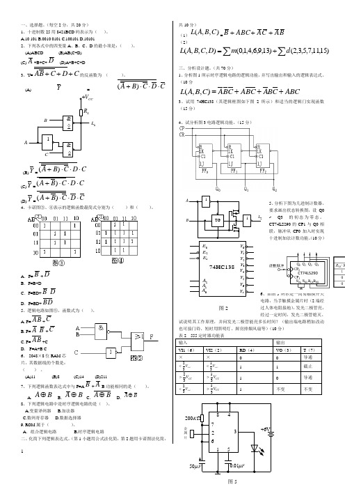
一、选择题。
(每空2分,共20分)1、十进制数25用8421BCD 码表示为( )。
A.10 101 B.0010 0101 C.100101 D .101012、下列各式中的四变量A 、B 、C 、D 的最小项是:( )。
(A)ABCD (B)AB(C+D) (C)A+B+C+D(D)A+B+C+D3、Y=A B C D C +++的反函数为 ( )。
(A)Y=()A B C D C+⋅⋅⋅A1L (B)Y =()A B C D C+⋅⋅⋅(C)Y =()A B C D C +⋅⋅⋅ (D)Y =()A B C D C+⋅⋅⋅4、卡诺图③、④表示的逻辑函数最简式分别为( )和( )。
A .F=B +DB .F=B+DC .F=BD +B DD .F=BD+BD5、逻辑电路如图⑤,函数式为( )。
A. F=AB +C B. F=A B +CC. F=AB+CD. F=A+B C6、 2048×8位RAM 芯片,其数据线的个数是:( ) 。
(A)11(B)8(C)14 (D)2117、下列逻辑函数表达式中与F=A B +AB 功能相同的是( )。
A.BA ⊕ B.BA ⊕ C.BA ⊕ D. AB ⊕8、下列逻辑电路中是时序逻辑电路的是( )。
A.变量译码器 B.加法器 C.数码寄存器 D.数据选择器 9. RO M 属于( )。
A .组合逻辑电路 B.时序逻辑电路二、化简下列逻辑表达式。
(第1小题用公式法化简,第2题用卡诺图法化简,共10分) (1)),,(C B A L =BA C A ABCB +++(2)∑∑+=)15,11,7,5,3,2()13,9,6,4,1,0(),,,(d m D C B A L三、分析设计题。
(共70分)1、分析图1所示时序逻辑电路的逻辑功能,并写出输出和输入的逻辑表达式。
(10分 (,,)L A B C ABC ABC ABC ABC=+++3、试用74HC138(其逻辑框图如下图2所示)和适当的逻辑门实现函数 (15分)4、试分析图3电路逻辑功能。
51单片机基础知识试题题库(含答案)
第二章习题参考答案一、填空题:1、当MCS-51引脚ALE有效时,表示从P0口稳定地送出了低8位地址。
2、MCS-51的堆栈是软件填写堆栈指针临时在片内数据存储器内开辟的区域。
3、当使用8751且EA=1,程序存储器地址小于 1000H 时,访问的是片内ROM。
4、MCS-51系统中,当PSEN信号有效时,表示CPU要从外部程序存储器读取信息。
5、MCS-51有4组工作寄存器,它们的地址范围是 00H~1FH 。
6、MCS-51片内20H~2FH范围内的数据存储器,既可以字节寻址又可以位寻址。
7、PSW中RS1 RS0=10时,R2的地址为 12H 。
8、PSW中RS1 RS0=11时,R2的地址为 1AH 。
9、单片机系统复位后,(PSW)=00H,因此片内RAM寄存区的当前寄存器是第 0 组,8个寄存器的单元地址为 00H ~ 07H 。
10、PC复位后为 0000H 。
11、一个机器周期= 12 个振荡周期= 6 个时钟周期。
12、PC的内容为将要执行的的指令地址。
13、在MCS-51单片机中,如果采用6MHz晶振,1个机器周期为 2us 。
14、内部RAM中,位地址为30H的位,该位所在字节的字节地址为 26H 。
15、若A中的内容为63H,那么,P标志位的值为 0 。
16、8051单片机复位后,R4所对应的存储单元的地址为 04H ,因上电时PSW=00H 。
这时当前的工作寄存器区是第 0 工作寄存器区。
17、使用8031芯片时,需将/EA引脚接低电平,因为其片内无程序存储器。
18、片内RAM低128个单元划分为哪3个主要部分:工作寄存器区、位寻址区和用户RAM区。
19、通过堆栈操作实现子程序调用,首先就要把 PC 的内容入栈,以进行断点保护。
调用返回时,再进行出栈保护,把保护的断点送回到 PC 。
20、MCS-51单片机程序存储器的寻址范围是由程序计数器PC的位数所决定的,因为MCS-51的PC是16位的,因此其寻址的范围为 64 KB。
迈瑞笔试题
1.数量级:1ns=__us,1Gs = ___Ms2.很简单的一个电路图,就不画了,也很简单。
3.摩尔定律是什么?它对硬件研发有什么影响。
(在Creative笔试中也考到过。
主要要记住是18到24个月这个重点)4.两个电路,要求分析电路功能以及输入输出关系。
一个就是典型的差分放大电路,一个是典型的积分电路。
很容易。
5.在高频电路中,电容等效于一个电感L,电容C以及一个电阻R,请问什么情况下电容才呈容性?这个只要总阻抗写出来,就明白怎么回事了。
6.一下子忘记了。
7.关于PCI读操作的时序英文翻译。
也很容易。
8.推理题。
9.1 AD前运放的跟随电路,要求找出电路的错误。
也就不画了。
9.2 JK触发器用verilog语言或者VHDL语言描述。
T触发器也就是J与K相连时特殊情况,用D触发器来实现。
这也很基本,很easy的。
9.3 好长,就不写了。
10. 描述一下你做过的一个电子设计原理图,遇到的问题以及解决思路。
这个VIA昨天也考过。
大家最好答详细点,因为迈瑞的监考官看了提前交卷的同学的卷子,感觉他们不太重视,实际上在阅卷时,可能这部分含金量很重。
硬件研发数字类1、锁相环输入25M 输出为CPLD连接。
要为25M、40M、65M、108M,写出锁相环内部需求的频率。
2、给出一张CPU及各存储器和IO的连接图。
都接到同一数据总线、时钟总线、地址总线。
100MHz时钟频率,说出不妥并改进3、给出一张en、clk和与门连接作为dff时钟沿的电路图。
给出不妥并改进。
4、翻译一段关于ddr3 sdram的E文,个人觉得难点在burst-oriented。
5、主观题。
简述一个做过的电子设计(软硬件皆可)的原理和实现,画出框图。
并简述遇到的问题和解决的思路。
联想笔试题1.设计函数int atoi(char *s)。
2.int i=(j=4,k=8,l=16,m=32); printf(“%d”, i); 输出是多少?3.解释局部变量、全局变量和静态变量的含义。
信息工程专业术语(16)
hacker 计算机迷 half adder 半加器 half byte 半字节 half current 半选电流 half duplex 半双向的 half duplex channel 半双向通道 half duplex circuit 半双⼯电路 half duplex line 半双⼯线路 half duplex operation 半双通信 half duplex transmission 半双⼯传输 half select 半选 half subtractor 半减器 half title 副标题 half tone 半⾳ half toning 半⾊导术 half word 半字 half word boundary 半字界 half word buffer 半字缓冲器 half write pulse 半写脉冲 hall device 霍⽿掐 hall effect 霍⽿效应 hall element 霍⽿掐 hall transducer 霍⽿传感器 halt 停⽌ halt address 停⽌地址 halt instruction 断点指令 halt key 停⽌键 halt point 断点 halt signal 停⽌信号 hamilton's function 哈密尔顿函数 hammer 印字锤 hamming code 汉秒 hamming distance 汉娩距 hand feed ⼿⼯馈送 hand feed punch ⼿⼯馈送穿孔机 hand held calculator ⼿提式计算器 hand held computer ⼿提式计算机 hand operation ⼿⼯操作⼈⼯操作 handler 处理程序 handling specification 操祖程 handshake 信号交换 handshaking 建⽴同步交换 handshaking protocol 信号交换协议 handshaking signal 认可信号 hang up 暂停 hard copy 硬拷贝 hard copy terminal 硬拷贝终端 hard disk 固定磁盘 hard error 硬错误 hard failure 硬失效 hard image 对⽐图象 hard sectored disk 硬扇⾯盘 hard stop 硬件停机 hardcore 核⼼硬件 hardware 硬件 hardware algorithm 硬件算法 hardware architecture 硬件总体结构 hardware check 硬件检验 hardware check point 硬件检验点 hardware compatibility 硬件兼容性 hardware component 硬件成分 hardware configuration 硬件配置 hardware costs 硬件费⽤ hardware design 硬件设计 hardware device 硬件部件 hardware division 硬件除法 hardware engineer 硬件⼯程师 hardware environment 硬件环境 hardware error 硬件错误 hardware failure 硬件故障 hardware independence 硬件独⽴性 hardware interrupt 硬件中断 hardware maintenance 硬件维修 hardware module 硬件模块 hardware multiplication 硬件乘法 hardware program 硬件程序 hardware redundancy 硬件冗余法 hardware reliability 硬设备可靠性 hardware representation 硬件表⽰ hardware restriction 硬件限制 hardware sprite 硬件⼦画⾯ hardware stack 硬件栈 hardware subprogram 硬件辅程序 hardware support 硬件⽀持 hardware system 硬件系统 hardwared automation 硬的⾃动化 hardwired knowledge 硬连线知识 hardwired logic 硬连线逻辑 hardwired subprogram 硬连线辅程序 harmonic analysis 谐波分析 harmonic analyzer 谐波分析仪 harmonic distortion 谐波失真 harmonic frequency 谐频 harmonic response characteristic 谐波响应特性 hartley 哈特利 hash ⽆⽤数据 hash addressing 散列寻址 hash chain 散列链 hash function 散列函数 hash table 散列表 hash total ⽆⽤数据总和 hashing 散列法 hashing function 散列函数 hazard rate 故障率 hdb ⾼密度双极编码 hdtv ⾼清晰度电视 hdx 半双向的 head 头 head crash 磁头碰撞 head gap 磁头缝隙 head per track disk 固定头磁盘 head processor 枝理机 head stack 磁头组 header 头部 header card 标题卡⽚ header label ⽂件始标 header line 标题⾏ header record 标题记录 header segment 标题段 header table 标题表 heading 头部 heap 堆 heap manager 堆管理 heat conduction 热传导 heat dissipation 热耗散 heat exchanger 热交换器 heat sensitive paper 热敏纸 heating coil 加热线圈 heavy duty software 重负载软件 heavy line 粗线 height balanced tree ⾼度平衡树 help 帮助 help information 求助信息 help library 求助库 help line 求助⾏ help menu 求助菜单 help mode 求助⽅式 help request 求助请求 help screen 帮助屏幕 hesitation 暂停 heuristic algorithm 启发式算法 heuristic approach 试探法 heuristic program 试探程序 heuristic programming 试探编程 heuristic routing 试探选路 heuristics 试探 hexadecimal constant ⼗六进制常数 hexadecimal digit ⼗六进制数字 hexadecimal format ⼗六进制格式 hexadecimal keyboard ⼗六进制键盘 hexadecimal notation ⼗六进制记数法 hexadecimal number ⼗六进制数 hexadecimal number system ⼗六进制记数制 hexadecimal system ⼗六进制 hf bus ⾼频母线 hidden fault 隐故障 hidden file 隐式⽂件 hidden line elimination 隐线消除 hidden line removal 隐线消除 hidden surface 隐⾯ hierarchical access method 分层存取法 hierarchical addressing 分层寻址 hierarchical database 分层数据库 hierarchical direct access method 分层直接存取法 hierarchical indexed direct access method 分层她直接存取法 hierarchical indexed sequential access method 分层她顺序存取法 hierarchical memory 分层存储器 hierarchical multicomputer system 分级多计算机系统 hierarchical network 层次络 hierarchical organization 分层结构 hierarchical sequential access method 分层顺序存取法 hierarchical structure 分层结构 hierarchy 分级 hierarchy chart 层次图 hierarchy memory 分层存储器 high bound 上界 high byte ⾼位字节 high definition television ⾼清晰度电视 high density bipolar coding ⾼密度双极编码 high density recording ⾼密度记录 high end computer ⾼级计算机 high level compiler ⾼级编译程序 high level computer ⾼级语⾔计算机 high level data link control ⾼级数据链路控制程序 high level goal ⾼级⽬标 high level language ⾼级语⾔ high level language computer ⾼级语⾔计算机 high level programming ⾼级程序设计 high level programming language ⾼级编程序语⾔ high level protocol ⾼级协议 high level signal ⾼电平信号 high order ⾼位 high order digit ⾼数位 high order language ⾼级语⾔ high order position ⾼位 high order zero ⾼位零 high performance computer ⾼性能计算机 high performance equipment ⾼性能设备 high performance mos ⾼性能⾦属氧化物半导体 high priority user ⾼优先⽤户 high resistance paper ⾼电阻纸 high resolution ⾼分辨率 high resolution graphics ⾼分辨率图 high resolution mode ⾼分辨率⽅式 high resolution timer ⾼分辨率计时器 high speed bus 快速总线 high speed carry ⾼速进位 high speed circuit ⾼速电路 high speed computer ⾼速计算机 high speed data network ⾼速数据络 high speed memory ⾼速存储器 high speed multiplication ⾼速乘法 high speed printer ⾼速打印机 high speed reader ⾼速输⼊机 high threshold logic ⾼阈值逻辑 high value resistor ⾼值电阻 high voltage level ⾼压电平 higher level language ⾼级语⾔ higher level module ⾼级模块 highest byte 字节 highest order 位 highway 局内线路 histogram 直⽅图 history 档案 history file 存档⽂件 hit 命中 hit on the fly printer 飞唤打印机 hit rate 命中率 hldlc ⾼级数据链路控制程序 hll ⾼级语⾔ hmos ⾼性能⾦属氧化物半导体 hold mode 保持状态 holding area 保存区 holding circuit 保持电路 holding register 保持寄存器存储寄存器 holding time 保持时间 hole 空⽳ hole conduction 空⽳导电 hole pattern 孔模 hollerith card 霍勒内斯卡⽚ hollerith code 霍勒内斯码 hollerith constant 霍勒内斯常数 hollerith machine 霍勒内斯计算机 hologram 全息照相 holographic memory 全息照相存储器 holographic retrieval 全息检索 home 出发点 home address 内部地址 home block 起始块 home channel 市内线路 home computer 家⽤计算机 home exchange 本地交换局 home key 起始键 home location 起始单元 home loop 本地回路 home position 原位 home record 起始记录 homography 同形异义性 homophone 同⾳字母 hook 钩 hop 转移 hopper 送卡箱 horizontal cursor 横向光标 horizontal feed ⽔平馈送 horizontal line ⽔平线 horizontal microinstruction 横向微指令 horizontal microprogramming 横向微程序设计 horizontal parity 横向奇偶 horizontal pointer 横向指⽰符 horizontal polarization ⽔平极化 horizontal processor 横向处理机 horizontal redundance check 横向冗余校验 horizontal tabulation 横向制表 horizontal tabulation character 横向制表字符 horn clause 霍队句 host bus 周线 host communications 与助通信 host computer 制算机 host language 诛⾔ host language processor 诛⾔处理程序 host machine 助 host processor 枝理机 host system 值统 hot line 热线 hot loop 热线 hot spare 热备件 hot standby 热备件 hot zone ⾏续区 housekeeping 内务操作 housekeeping data 内务数据 housekeeping information 内务信息 housekeeping instruction 内务指令 housekeeping operation 内务操作 housekeeping routine 内务程序 housing 箱 hrt ⾼分辨率计时器 ht 横向制表 htl ⾼阈值逻辑 hub 磁盘套 hue ⾊调 hull 外壳 human computer interface ⼈机接⼝ human engineering ⼯效学 human factor ⼈员因素 human factor error ⼈错误 human failure ⼈为失效 human oriented language ⾯向⼈的语⾔ hunting 不规则振荡 hybrid circuit 混合电路 hybrid computer 混合计算机 hybrid database 混合数据库 hybrid integrated circuit 混合集成电路 hybrid microcircuit 混合微电路 hybrid network 混合络 hybrid packaging 混合组装 hybrid system 混合系统 hypercube 超⽴⽅ hypermedia 超媒体 hypertext 超级正⽂ hypervisor 超级监视者 hyphen 连字符 hyphenation 连字符连接 hypothetical reference circuit 假设基准电路 hypothetical world 假想世界 hysteresis 滞后现象 hysteresis curve recorder 滞后曲线记录器 hysteresis error 滞后特性误差 hysteresis loop 滞后回线 hysteresis loop recorder 滞后曲线记录器 hysteresis meter 滞后测定器 i/o 输⼊输出 i/o bound task 受输⼊输出限制的任务 i/o buffer 输⼊输出缓冲器 i/o bus 输⼊输出总线 i/o bus controller 输⼊输出总线控制器 i/o channel 输⼊输出通道 i/o control 输⼊输出控制 i/o control program 输⼊输出控制程序 i/o control system 输⼊输出控制系统 i/o conversion 输⼊输出数据型转换 i/o data 输⼊输出数据 i/o limited program 受输⼊输出限制的程序 i/o operation 输⼊输出操作 i/o port 输⼊输出⼝ ia 指令地址 ibm ibm ibm compatible computer ibm 兼容机 ic 集成电路 ic chip 集成电路⽚ ic computer 集成电路计算机 ic memory 集成电路存储器 ic socket 集成电路插孔 ic tester 集成电路测试机 icon 图标 iconic representation 图象表⽰ id 识别码 ideal value 理想值 idealized system 理想化系统 ident 识别 identical transformation 恒等变换 identification 识别 identification byte 标识字节 identification card 标识卡⽚ identification character 标识字符 identification code 识别码 identification division 识别部分 identifier 标识符 identify element 全同元件 identifying information 识别信息 identity 等同 identity gate 同门 identity operation 全同运算 identity unit 全同单元 idle channel 空闲通道 idle character ⽆效字符 idle mode 空闲状态 idle state 空闲状态 idle time 空闲时间 idn 综合数字 idp 集中数据处理 if statement 如果语句 if then operation 蕴含操作 ifip 国际信息处理联合会 il 等平⾯集成注⼊逻辑 il technology il 技术 illegal access ⾮法存取 illegal access protection ⾮法存取保护 illegal character ⾮法字符 illegal code ⾮法代码 illegal command check ⾮法命令校验 illegal instruction ⾮法指令 illegal operation ⾮法操作 illegal symbol ⾮法符号 image 图象 image copy 图象副本 image dissector 析像器图像传感器 image file 图象⽂件 image generation 图象⽣成 image graphics 图象图形 image memory 图象存储器 image processing 图象处理 image processor 图象处理机 image regeneration 再⽣ image restoration 图象复原 image sensor 图象传感器 image store 图象存储 image transmission 视频传输 image understanding 图象理解 imager 图象机 imaginary number 虚数 imaginary part 虚数部 immediate access ⽴即存取 immediate access memory ⽴即存取存储器 immediate access storage ⽴即存取存储器 immediate address ⽴即地址 immediate addressing ⽴即寻址 immediate answer ⽴即应答 immediate command ⽴即命令 immediate data 直接数据 immediate instruction ⽴即指令 immediate mode ⽴即⽅式 immediate operand ⽴即操 immediate predecessor relation 直接先秦系 immediate processing 直接处理 impact printer 或式打印机 impact printing 或式印刷 imparity check 奇数奇偶性较验 impedance 阻抗 imperative go to statement 强制go to语句 imperative language 强制性语⾔ imperative statement 强制语句 imperfect tape 缺陷带 implementation 执⾏ implementation specification 实现规格 implementator 实现者。
FPGA及ASIC笔试题库
1、我们公司的产品是集成电路,请描述一下你对集成电路的认识,列举一些与集成电路相关的内容(如讲清楚模拟、数字、双极型、CMOS、MCU、RISC、CISC、DSP、ASIC、FPGA等的概念)。
(仕兰微面试题目)2、FPGA和ASIC的概念,他们的区别。
(未知)答案:FPGA是可编程ASIC。
ASIC:专用集成电路,它是面向专门用途的电路,专门为一个用户设计和制造的。
根据一个用户的特定要求,能以低研制成本,短、交货周期供货的全定制,半定制集成电路。
与门阵列等其它ASIC(Application Specific IC)相比,它们又具有设计开发周期短、设计制造成本低、开发工具先进、标准产品无需测试、质量稳定以及可实时在线检验等优点3、什么叫做OTP片、掩膜片,两者的区别何在?(仕兰微面试题目)4、你知道的集成电路设计的表达方式有哪几种?(仕兰微面试题目)5、描述你对集成电路设计流程的认识。
(仕兰微面试题目)6、简述FPGA等可编程逻辑器件设计流程。
(仕兰微面试题目)7、IC设计前端到后端的流程和eda工具。
(未知)8、从RTL synthesis到tape out之间的设计flow,并列出其中各步使用的tool.(未知)9、Asic的design flow。
(威盛VIA 2003.11.06 上海笔试试题)10、写出asic前期设计的流程和相应的工具。
(威盛)11、集成电路前段设计流程,写出相关的工具。
(扬智电子笔试)先介绍下IC开发流程:1.)代码输入(design input)用vhdl或者是verilog语言来完成器件的功能描述,生成hdl代码语言输入工具:SUMMIT VISUALHDLMENTOR RENIOR图形输入: composer(cadence);viewlogic (viewdraw)2.)电路仿真(circuit simulation)将vhd代码进行先前逻辑仿真,验证功能描述是否正确数字电路仿真工具:Verolog: CADENCE Verolig-XLSYNOPSYS VCSMENTOR Modle-simVHDL : CADENCE NC-vhdlSYNOPSYS VSSMENTOR Modle-sim模拟电路仿真工具:***ANTI HSpice pspice,spectre micro microwave: eesoft : hp3.)逻辑综合(synthesis tools)逻辑综合工具可以将设计思想vhd代码转化成对应一定工艺手段的门级电路;将初级仿真中所没有考虑的门沿(gates delay)反标到生成的门级网表中,返回电路仿真阶段进行再仿真。
- 1、下载文档前请自行甄别文档内容的完整性,平台不提供额外的编辑、内容补充、找答案等附加服务。
- 2、"仅部分预览"的文档,不可在线预览部分如存在完整性等问题,可反馈申请退款(可完整预览的文档不适用该条件!)。
- 3、如文档侵犯您的权益,请联系客服反馈,我们会尽快为您处理(人工客服工作时间:9:00-18:30)。
IEEE JOURNAL OF QUANTUM ELECTRONICS, VOL 26, NO 4. APRIL
1990
619
Quantum Electronics Letters
A Rapid Optoelectronic Half-Adder Logic Composed of a Pair of GaAs
Metal-Semiconductor-Metal Photodetectors
KAZUTOSHI NAKAJIMA, TAKASHI IIDA, KEN-ICHI SUGIMOTO, HIROFUMI KAN, AND
YOSHIHIKO MIZUSHIMA
Absfrucf-A novel optoelectronic half-adder logic, composed of only two GaAs metal-semiconductor-metal photodetectors (MSM-PD’s), is reported. The optoelectronic logic is made to utilize the feature of the MSM-PD, which has a symmetrical Schottky contact structure which
operates for both polarities of electrical bias (positive and negative). Without any other active devices like transistors, the output delay time is short, less than 100 ps, which assures a very fast arithmetic opera-
tion.
I. INTRODUCTION ECENTLY, several optical computing systems and R
their component devices have been reported [ 11-[3]. In this letter, we report a novel rapid optoelectronic half- adder logic. The inputs are optical signals, and the results are electrical signals. The output can be fed to laser diodes
converting into optical signals, thus optical input-output is easily realizable. By a tandem connection of this half-adder logic ele- ments, a full-adder is also possible, which will be re- ported later. Here we describe the essential feature of this one-bit half-adder for optical inputs. The half-adder is basically composed of only two GaAs metal-semiconductor-metal photodetectors (MSM-PD’s). Without any other active devices such as transistors, the optoelectronic logic is able to operate at an ultrahigh speed, since its capacitance is minimized. The GaAs MSM-PD has features of an ultrahigh speed, while the symmetrical Schottky contact structure allows a bias ap- plication in either polarity [4]-[ 111. The electrical output signals are generated in a polarity corresponding to the bias. Moreover, the planar structure of the MSM-PD is very suitable for monolithic integration [ 121-[18].
11. CIRCUIT FABRICATION AND OPERATION The optoelectronic half-adder logic circuit is shown in Fig. 1. For simplicity, the following experiment is per-
formed using discrete details. We show that even with such a preliminary setup on a table, a promising result can be obtained. Two GaAs MSM-PD’s are provided as the input gates for two optical signals. To each of the MSM- PD’s, 5 V biases with mutually opposite polarities, (V,)
Manuscript received July 3, 1989; revised November 10, 1989. The authors are with Hamamatsu Photonics, Hamamatsu 435, Japan.
IEEE Log Number 8933806.
Fig. 1. Optical half-adder logic gate composed of two GaAs
MSM-PD’s,
with resistances and a capacitance.
and (V,) are applied. As shown in Fig. 2, the MSM-PD has a 200 pm square active area. A pair of symmetrical Schottky contact electrodes are disposed interdigitally, on an undoped epitaxial GaAs substrate. Both the rise and falltimes are less than 50 ps for a 50 Cl load resistance.
The positive current signal generated at the electrode (a2) of MSM-PD (A) is divided at a point (4). Part of it is transferred to the SUM output terminal through the re- sistance ( RI ) and the other to the CARRY output terminal
through the resistance (R2). In order that the current sig- nal is equally divided at the point (q), these resistances
have the same magnitude. On the other hand, the negative current signal generated at the electrode (b, ) of MSM-PD (B) is transferred to the
SUM output terminal, and the positive current signal gen- erated at the electrode ( b2 ) is transferred to the CARRY
output terminal. The resistance (R2) must not be much
smaller than the load resistance at the output terminal, otherwise the resistance acts as a shunt for the MSM-PD (B) and the signal from the MSM-PD (B) becomes too small. If it is too large, the response time becomes slow. We choose 50 Cl for R2 and RI, which is the same as the load resistance. Resistance (R3) and capacitance (C) are for bias-blocking. The SUM output signal is obtained at a point (p) by an
XOR logic, from the electrode (a2) of MSM-PD (A) and (b, ) of MSM-PD (B). Because these electrical signals
are of the opposite polarities, the electrical signals from two MSM-PD’s cancel each other at the point (p). On
0018-9197/90/0400-0619$01 .OO 0 1990 IEEE