A 1.0V GHz Range 0.13um CMOS Frequency Synthesizer
DS8913中文资料
TL F 7398DS8911 DS8913AM FM TV Sound Up-Conversion Frequency SynthesizerApril 1990DS8911 DS8913AM FM TV Sound Up-Conversion Frequency SynthesizerGeneral DescriptionThe DS8911is a digital Phase-Locked Loop (PLL)frequen-cy synthesizer intended for use as a Local Oscillator (LO)in electronically tuned radios The device is used in conjunc-tion with a serial data controller a loop filter some varactor diodes and several passive elements to provide the local oscillator function for both AM and FM tuningThe conventional superheterodyne AM receiver utilizes a low IF or down conversion tuning approach whereby the IF is chosen to be below the frequencies to be received The DS8911PLL on the other hand utilizes an up-conversion technique in the AM mode whereby the first IF frequency is chosen to be well above the RF frequency range to be tuned This approach eliminates the need for tuned circuits in the AM frontend since the image half IF and other spuri-ous responses occur far beyond the range of frequencies to be tuned Sufficient selectivity and second IF image protec-tion is provided by a crystal filter at the output of the first mixerA significant cost savings can be realized utilizing this up-conversion approach to tuning Removal of the AM tuned circuits eliminates the cost of expensive matched varactor diodes and reduces the amount of labor required for align-ment down from 6adjustments to 2 Additional cost savings are realized because up-conversion enables both the AM and FM bands to be tuned using a single Voltage Controlled Oscillator (VCO)operating between 98and 120MHz (The 2to 1LO tuning range found in conventional AM down con-version radios is reduced to a 10%tuning range 9 94MHz to 11 02MHz)Up-conversion AM tuning is accomplished by first dividing the VCO signal down by a modulus 10to obtain the LO signal This LO in turn is mixed on chip with the RF signal to obtain a first IF at the MIXER output pins This first IF after crystal filtering is mixed (externally)with a reference fre-quency provided by the PLL to obtain a 450kHz second IFfrequency The DS8911derives the 450kHz second IF by mixing an 11 55MHz first IF with a 12 00MHz reference frequencyFM and WB (weather band)tuning is done using the con-ventional down conversion approach Here the VCO signal is buffered to produce the LO signal and then mixed on chip with the RF signal to obtain an IF frequency at the MIXER output pins This IF frequency is typically chosen to be 10 7MHz although placement at 11 50MHz can further enhance AM mode performance and minimize IF circuitryThe PLL provides phase comparator reference frequencies of 10 12 5 25 and 100kHz The tuning resolutions result-ing from these reference frequencies are determined by di-viding the reference by the premix modulus Table II shows the tuning resolutions possibleThe DS8911contains the following logic elements a volt-age controlled oscillator a reference oscillator a 14-bit pro-grammable dual-modulus counter a reference frequency di-vider chain a premix divider a mixer a phase comparator a charge pump an operational amplifier and control circuitry for latched serial data entryThe DS8913includes all the above logic elements except that it requires a 10MHz reference frequency instead of 12MHzFeaturesY Direct synthesis of LW MW SW FM and WB frequenciesY Serial data entry for simplified processor control Y 10 12 5 25 and 100kHz reference frequencies Y 8possible tuning resolutions (see Table II)Y An op amp with high impedance inputs for loop filtering YProgrammable mixer with high dynamic rangeTRI-STATE is a registered trademark of National Semiconductor Corporation MICROWIRE TM is a trademark of National Semiconductor Corporation C 1995National Semiconductor CorporationRRD-B30M105 Printed in U S AConnection DiagramPlastic Chip CarrierTL F 7398–8Top ViewOrder Number DS8911V DS8913VSee NS Package Number V28APin DescriptionsV CC1 The V CC1pin provides a5V supply source for all circuitry except the reference divider chain op amp and mix-er sections of the dieV CC2 The V CC2pin provides a12V supply source for the Op ampV CCL The V CCL pin provides an isolated5V supply source for the premix divider and mixer functionsV CCM The V CCM pin provides a5V supply source for the reference oscillator and divider chain down through the50 Hz output thus enabling low standby current for time-of-day clock applicationsGND1 GND2 GNDL and GNDM Provide isolated circuit ground for the various sections of the deviceDATA and CLOCK The DATA and CLOCK inputs are for serial data entry from a controller They are CMOS inputs with TTL logic thresholds The24-bit data stream is loaded into the PLL on the positive transition of the CLOCK The first14bits of the data stream select PLL divide code in binary form MSB first The15th through24th bits select the premix modulus the reference frequency the bit output status and the test operate modes as shown in Tables I through VENABLE The ENABLE input is a CMOS input with a TTL logic threshold The ENABLE input enables data when at a logic‘‘one’’and latches data on the transition to a logic ‘‘zero’’BIT Outputs The open-collector BIT outputs provide either the status of shift register bits22 23 and24or enable access to key internal circuit test nodes The mode for the bit outputs is controlled by shift register bits20and21 In operation the bit outputs are intended to drive radio func-tions such as gain mute and AM FM status These outputs can also be used to program the loop gain by connection of an external resistor to IPROG Bit24output can also be used as a300millisecond timer under control of shift regis-ter bit19 During service testing these pins can be used for the purpose of either monitoring or driving internal logic points as indicated in the TEST MODES description under Table VVCOb and VCOe The Voltage Controlled Oscillator inputs drive the14-bit programmable counter and the premix divid-er These inputs are the base and emitter leads of a transis-tor which require connection of a coil varactor and several capacitors to function as a Colpitts oscillator The VCO is designed to operate up to225MHz The VCO’s minimum operating frequency may be limited by the choice of refer-ence frequency and the961minimum modulus constraint of the31 32dual modulus counterRF a and RF b The Radio Frequency inputs are fed differ-entially into the mixerIMXR The bias current for the mixer is programmed by con-nection of an external resistor to this pin The total mixer output current equals4times the current entering this pin MIXER and MIXER The MIXER outputs are the collectors of the double balanced pair mixer transistors They are in-tended to operate at voltages greater than V CC1OSCb and OSCc The Reference Oscillator inputs are part of an on-chip Pierce oscillator designed to work in conjunc-tion with2capacitors and a crystal resonator The DS8911 requires a12MHz crystal to derive the reference frequen-cies shown in Table II The DS8913requires10MHz crystal The12MHz OSC signal is also used externally as the2nd AM LO to obtain a450kHz2nd IF frequency in the AM mode2MHz The2MHz output is provided to drive a controller’s clock input50Hz The50Hz output is provided as a time reference for radios with time-of-day clocksIPROG The IPROG pin enables the charge pump to be programmed from0 25mA to1 0mA by connection of an external resistor to groundCPO The Charge Pump Output circuit sources current if the VCO frequency is high and sinks current if the VCO frequen-cy is low The CPO is wired directly to the negative input of the loop filter op ampOP AMP The OP AMP output is provided for loop filtering The op amp has high impedance PMOS gate inputs and is wired as a transconductance amplifier filter The op amp’s positive input is internally referenced while its negative input is common with the CPO output2Reference TablesTABLE IBit15Premix Modulus0d11d10TABLE IIBit Reference Tuning Resolution 1617Frequency d1Premix d10Premix 0010kHz10kHz1kHz 0112 5kHz12 5kHz1 25kHz 1025kHz25kHz2 5kHz 11100kHz100kHz10kHzTABLE IIIBit18Mode0Normal Operation1Production Test Mode OnlyThe user should always load Bit18lowTABLE IVBit19Timer0Bit24Status1Bit24for300msTIMER OPERATIONThe timer function is provided for use as a retriggerable ‘‘one shot’’to enable muting for approximately300millisec-onds after station changes The timer is enabled at bit24’s output if the normal operating mode is selected(shift regis-ter bits20and21e‘‘LOW’’)and shift register bit19data is latched as a‘‘HI’’ The timer’s output state will invert imme-diately upon latching bit19‘‘HI’’and remain inverted for approximately300milliseconds If the user readdresses the device with bit19data‘‘LOW’’before the timer finishes itscycle the timer’s BIT24output will finish out the300ms pulse Readdressing the device with bit19‘‘HI’’before the timer finishes its cycle will extend the BIT24output pulse width by300ms Addressing should be performed immedi-ately after the50Hz output transitions‘‘HI’’ BIT24’s output state is not guaranteed during the first300ms after V CC1 power up as a result of a timer reset in progressTABLE VBit FUNCTION OF2021PINS3 4 500Status of Bits22-2401Test mode110Test mode211Test mode3 TEST MODE OPERATIONTest Mode1 Enables the BIT output pins to edge trigger the phase comparator inputs and monitor an internal lock detector BIT22negative edge triggers the reference divid-er input of the phase comparator if the reference divider state is low BIT23provides the open collector ORing of the phase comparator’s pump up and down outputs BIT24 negative edge triggers the N counter input of the phase comparator if the N counter state is preconditioned lowTest Mode2 Enables the BIT outputs to clock the pro-grammable N counter monitor its output and force either its load or count condition BIT22provides the N counter out-put which negative edge triggers the phase comparator and which appears low one N counter clock pulse before it re-loads BIT23positive edge triggers the N counter’s clock input if the prescaler’s output is preconditioned HI BIT24 clears the N counter output so that loading will occur on the next N counter clock edgeTest Mode3 Enables the BIT outputs to clock the50Hz and10kHz reference dividers and monitor the reference divider input to the phase comparator BIT22positive edge clocks the10kHz reference divider chain if the10kHz out-put is preconditioned HI BIT23positive edge clocks the50 Hz divider chain BIT24is the reference divider negative edge trigger input to the phase comparator3Absolute Maximum Ratings(Note1)If Military Aerospace specified devices are required please contact the National Semiconductor Sales Office Distributors for availability and specifications Supply VoltageV CCM7V V CC17V V CC215V Input Voltage7V Output VoltageLogic7V Op Amp and Mixer Outputs15V ESD Sensitivity1000V Storage Temperature Range b65 C to a150 C Lead Temp (Soldering 10seconds)300 C Operating ConditionsMin Max Units V CCM3 55 5VV CC14 55 5VV CC27 012 0V Temperature T A b40a85 C Mixer I BIAS(Mixer a Mixer Current)120mADC Electrical Characteristics(Notes2and3)Symbol Parameter Test Conditions Min Typ Max Units V IH Logic‘‘1’’Input Voltage2 0VV IL Logic‘‘0’’Input Voltage0 8VI IH Logic‘‘1’’Input Current V IN e5 5V10m A I I Logic‘‘1’’Input Current Data Clock and Enable Inputs V IN e7V100m A I IL Logic‘‘0’’Input Current Data Clock and Enable Inputs V IN e0V b10m A V OH Logic‘‘1’’2MHz I OH e b20m A V CCM b0 3V Output VoltageI OH e b400m A V CCM b2VOp Amp I OH e b1 0mA V CC2b1 5VV OL Logic‘‘0’’2MHz I OL e20m A0 3V Output VoltageI OL e400m A0 4V50Hz I OL e250m A0 3VBit Outputs I OL e1mA0 3VOp Amp I OL e1 0mA1 5VV BIAS Op Amp Input V D Op Amp I O Shorted V CC1e5 5V V CC2e12V 200mVCPO e TRI-STATE Op Amp I OH vs I OL AppliedI CEX High Level Bit Outputs V CC1e4 5V V O e8 8V100m AOutput Current50Hz V CCM e3 5V V O e5 5V10m AMixers V CCL e V CC1e4 5V V O e12V100m A I CPO Charge Pump Program0 25mA k I CPO k1 0mA Pump-up b302I PROG a30%Current2I PROG e V CC1 R PROGPump-down b302I PROG a30%Measured I PROG to CPOTRI-STATE0100nA I CCM V CCM Supply Current V CCM e5 5V OSCC e High0 51 0mA(Static)I CC1a V CC1a V CCL V CC e5 5V Bits Hi I MXR and I PROG Open2535mA I CCL Supply CurrentI CC2V CC2Supply Current V CC2e12V1 52 5mA Mixer Mixer a Mixer V CC1e V CCL e5 5V Mixer e Mixer e12V b254IMXR a25% I BIAS Current(Note4)RF IN Mixer Input Max Mixer I BIAS e20mA300mVrms Signal Level RF a or RF b Signal LevelNote1 ‘‘Absolute Maximum Ratings’’are those values beyond which the safety of the device cannot be guaranteed Except for‘‘Operating Temperature Range’’ they are not meant to imply that the device should be operated at these limitsNote2 Unless otherwise specified min max limits apply across the b40 C to a85 C temperature rangeNote3 All currents into device pins are shown as positive out of device pins as negative all voltage referenced to ground unless otherwise noted All values shown as maximum or minimum on absolute value basisNote4 Total mixer output current(Mixer a Mixer)j4times the current into the I MXR pin4AC Electrical Characteristics(Note2)Symbol Parameter Conditions Min Typ Max Units t r20%–80%Rise Time200ns t f80%–20%Fall Time200ns DATA SU Data Setup Time100ns DATA H Data Hold Time100nsV CC1e4 5V to5 5VEN SU Enable Setup Time100ns EN H Enable Hold Time100ns EN PW a Enable Positive Pulse Width200ns CLK PW a Clock Positive Pulse Width200ns CLK PW b Clock Negative Pulse Width200ns VCO f max VCO Max Frequency See Typical Wiring Diagram20225MHz OSC f max Reference Oscillator V CCM e3 5V12MHz Max FrequencyTiming DiagramTL F 7398–10 MICROWIRE TM Bus FormatTL F 7398–195TABLE VI DS8911Tuning CharacteristicsIF Tuning VCOPremix Reference TuningImageMode Frequency Range RangeModulus Frequency Resolution(MHz)(MHz)(MHz)(MHz)(kHz)(kHz)LW11 55 450 145– 290112 4–114 11010122–23 MW11 55 450 515–1 6199 4–110 21010 12 5 25 1001 1 25 2 5 1021–23 SW11 55 4505 94–6 253 5to56 11010 12 5 251 1 25 2 528–30 FM10 787 4–108 198 1–118 8110 12 5 25 10010 12 5 25 100109–130 WB10 7162 4–162 6151–152112 5 2512 5 25140–142 TV110 759 75–87 7570 45–98 451252581–109 TV210 7179 75–215 75169 1–205 112525158–194Input and Output SchematicsTL F 7398–11TL F 7398–126Input and Output Schematics (Continued)TL F 7398–13TL F 7398–14TL F 7398–15TL F 7398–16TL F 7398–17TL F 7398–187Logic DiagramDS8911 DS8913PLL SynthesizerTL F 7398–4 Note1 The14bit programmable N counter is a dual modulus counter with31 32prescaler The minimum continuous modulus of the N counter is 961 (There are a limited number of valid modulus codes below961 )The DS8913has d5Typical Application DiagramAM FM ETR Radio ApplicationTL F 7398–58Wiring DiagramsConfiguration Using PLL and First Mixer FunctionsTL F 7398–20Configuration Using PLL with LO Bypassing MixerThe mixer is de-biased by the100X resistor on the RF apin to act as an output bufferfor the LO signalTL F 7398–219D S 8911 D S 8913A M F M T V S o u n d U p -C o n v e r s i o n F r e q u e n c y S y n t h e s i z e rPhysical Dimensions inches (millimeters)Lit 103661Plastic Chip Carrier (V)Order Number DS8911V DS8913VNS Package Number V28ALIFE SUPPORT POLICYNATIONAL’S PRODUCTS ARE NOT AUTHORIZED FOR USE AS CRITICAL COMPONENTS IN LIFE SUPPORT DEVICES OR SYSTEMS WITHOUT THE EXPRESS WRITTEN APPROVAL OF THE PRESIDENT OF NATIONAL SEMICONDUCTOR CORPORATION As used herein 1 Life support devices or systems are devices or 2 A critical component is any component of a life systems which (a)are intended for surgical implant support device or system whose failure to perform can into the body or (b)support or sustain life and whose be reasonably expected to cause the failure of the life failure to perform when properly used in accordance support device or system or to affect its safety or with instructions for use provided in the labeling can effectivenessbe reasonably expected to result in a significant injury to the userNational Semiconductor National Semiconductor National Semiconductor National Semiconductor CorporationEuropeHong Kong LtdJapan Ltd1111West Bardin RoadFax (a 49)0-180-530858613th Floor Straight Block Tel 81-043-299-2309。
Silicon Labs EFM8BB2 MCU数据手册(中文版)

Serial Interfaces
2 x UART
SPI
I2C / SMBus
High-Speed I2C Slave
I/O Ports
External Interrupts
Pin Reset
General Purpose I/O
Pin Wakeup
8-bit SFR bus
Timers and Triggers
CMOS Oscillator Input
Port I/O Configuration
Digital Peripherals
UART0 UART1
Timers 0, 1, 2, 3, 4
3-ch PCA
I2C Slavbar Decoder
SPI CRC
Clock Management
External CMOS Oscillator
High Frequency 49 MHz RC Oscillator
Energy Management
Internal LDO Regulator
Power-On Reset
Flash Program Memory
(16 KB)
15
10
7
Yes —
-40 to +85 QFN20 C
| Smart. Connected. Energy-friendly.
Preliminary Rev. 0.2 | 2
3. 系统概述
3.1 简介
EFM8BB2 数据表
系统概述
C2CK/RSTb
VDD VREGIN
GND
C2D
Reset
Power-On Reset
A7139手册
1.典型应用■ ISM频段数据通信;■家居安全;■ 无线远程控制; ■ 无线传感器网络■ RKE(远程无钥匙进入)■能量控制和管理■建筑自动化 ■AMR2.一般描述A7139为全集成低中频结构CMOS FSK/GFSK TRX,可运行在315/433/470/510/868/915MHz 的ISM频段。
本芯片特别适用于电池供电的470~510MHz频段的中国AMR和868.3MHz的欧洲M-bus。
A7139为笙科最小功耗系列亚GHz ISM频段产品,其具有非常低的功耗(如,434MHz频段,RX模式下功耗为3.8mA)。
而且,A7139能够提供非常好的链路预算,高效E类功放输出功率高达20dBm,以及非常低的相位噪声(-110dBm RX接收灵敏度@ 100Kbps/ FSK/ 433.92MHz)。
因此,A7139非常适合电池供电视距距离无线传输。
A7139包括了一个基带调制解调器可以进行数据率可编程从2K到250Kbps。
对于电池供电系统,A7139支持快速PLL启动时间(120us),Xtal启动时间(1100us)和片上稳压器启动时间(850us)以减少平均功耗。
RF综合器包括了VCO和低噪声小数PLL,其频率分辨率达366Hz。
由于A7139是低中频结构TRX其IFBW可编程(IF滤波器带宽,50kHz/100KHz/150KHz/250KHz),RXLO必须根据IFBW设置配置成与TXRF偏差一个IF。
A7139控制寄存器通过3线或4线SPI接口访问,包括TX/RFFIFO、VCO频率、片上校准过程。
另一方面,通过SPI,可以发出唯一的Strobe命令,可以控制A7139功耗模式(深睡眠、睡眠、空闲、待机)、PLL模式、TX模式和RX模式。
和SPI一起,A7139和MCU之间的数字连接为GIO1和GIO2(最少功能GPIO),可用于指示A7139状态,因此MCU可以用于轮流检测或射频控制中断。
TPA6132A2规格书
OUTR+
OUTRCODEC
OUTL+
OUTL-
ENABLE GAIN0 GAIN1 VBAT
INR+
INR-
OUTR
TPA6132A2
INL+
OUTL
INL-
EN G0 G1 VDD
HPVDD CPP
SGND PGND
HPVSS CPN
1
Please be aware that an important notice concerning availability, standard warranty, and use in critical applications of Texas Instruments semiconductor products and disclaimers thereto appears at the end of this data sheet. DirectPath is a trademark of Texas Instruments.
These devices have limited built-in ESD protection. The leads should be shorted together or the device placed in conductive foam during storage or handling to prevent electrostatic damage to the MOS gates.
25-mW DIRECTPATH™ STEREO HEADPHONE AMPLIFIER WITH POP SUPPRESSION
FEATURES
1
•23 Patented DirectPath™ Technology Eliminates Need for DC-Blocking Capacitors – Outputs Biased at 0 V – Excellent Low Frequency Fidelity
AD9680中文资料
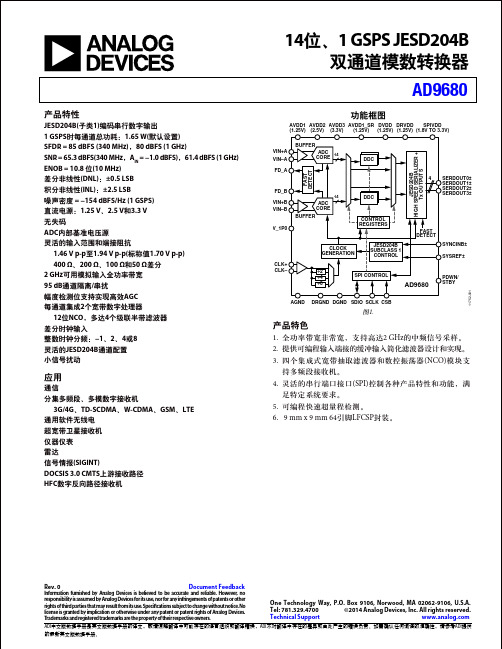
应用
通信 分集多频段、多模数字接收机 3G/4G、TD-SCDMA、W-CDMA、GSM、LTE 通用软件无线电 超宽带卫星接收机 仪器仪表 雷达 信号情报(SIGINT) DOCSIS 3.0 CMTS上游接收路径 HFC数字反向路径接收机
Rev. 0
Information furnished by Analog Devices is believed to be accurate and reliable. However, no responsibility is assumed by Analog Devices for its use, nor for any infringements of patents or other rights of third parties that may result from its use. Speci cations subject to change without notice. No license is granted by implication or otherwise under any patent or patent rights of Analog Devices. Trademarks and registered trademarks are the property of their respective owners.
CLK+ CLK–
÷2 ÷4 ÷8
SPI CONTROL
AD9680
PDWN/ STBY
11752-001
AGNDΒιβλιοθήκη DRGND DGND SDIO SCLK CSB
图1.
产品特色
1. 全功率带宽非常宽,支持高达2 GHz的中频信号采样。 2. 提供可编程输入端接的缓冲输入简化滤波器设计和实现。 3. 四个集成式宽带抽取滤波器和数控振荡器(NCO)模块支 持多频段接收机。 4. 灵活的串行端口接口(SPI)控制各种产品特性和功能,满 足特定系统要求。 5. 可编程快速超量程检测。 6. 9 mm x 9 mm 64引脚LFCSP封装。
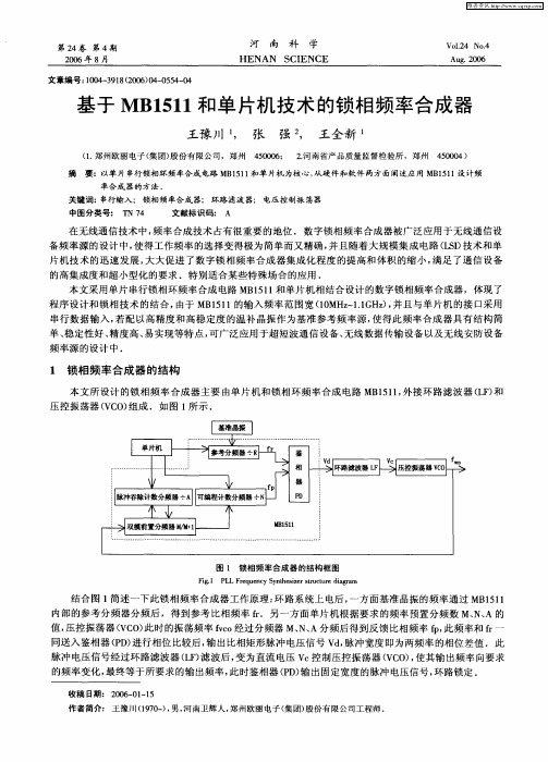
基于MB1511和单片机技术的锁相频率合成器
收 稿 日期 : 20 一 1 1 06O— 5
作者简介: 王豫川 (9 0 ) 男, 17 一 , 河南卫辉 人, 郑州欧丽 电子 ( 团) 份有 限公司工程师 . 集 股
片机 技 术 的迅 速 发展 , 大大 促 进 了数 字 锁 相频 率 合成 器 集 成化 程 度 的提 高和 体积 的缩 小 , 满足 了通 信 设 备 的高 集成 度和 超 小型 化 的要 求 .特 别适合 某 些特 殊场 合 的应用 .
本文 采用 单 片 串行 锁相 环 频率 合成 电路 MB 5 和单 片机 相 结合 设计 的数 字锁 相频 率合 成器 ,体 现 了 11 1
片 , 用贴 片 S O 采 S P超 小型封 装 .其 主要 特 点 为:
①低 电压供 电: C = . 一 . ; V C 2 V 5 V ②高工作频率 :nm x 1 G z i m n 一 0B )③具有脉冲吞除功 7 5 i f a = . H ( n i 1d m ; 1 V = 能: / ,2/2 ; 串行输入 1 位可编程分频器包括 : 6 6 1819④ 45 8 二进制 7 位脉冲吞除计数器:— 2 ; 0 17 二进制 1 位可 1 编程计数器 :6 24 ; 串行输入 1 位可编程分频器包括: 1— 07⑤ 5 二进制 1 位可编程 参考计数器 :— 6 8 , 位 4 8 13 3 1 开关计数器用来设置前置分频器的预分频 比; 种鉴相器输出: 内充电泵 ( ⑥2 片 双极性) 出和外接充电泵输 输 出; 宽温工作范围:4 ℃~ 8℃. ⑦ -O 十O
振 荡器 等 , 体 的 设计 可 参 考有 关 技 术 书籍 , 具 本文 不 再 介 绍 .这 里 着 重 介 绍 MB 5 单 片机 硬 件 接 口 电 11 1和 路 的设计 和 软件 的实现 方法 .
锁相环频率合成器—LC72131
TEL:0755-8286387713242913995E-MAIL:*****************锁相环频率合成器—LC72131概述与特点LC72131是一种锁相环频率合成器。
该电路的特点如下:1.高速可编程分频器FMIN: 10--160MHz……………双模式预分频(内置二分频器)AMIN: 2--40MHz ……………双模式预分频0.5--10MHz ……………直接分频2. 计数器IFIN: 0.4--12MHz ……………AM/FM中频计数3.参考频率十二个可选择的参考频率(4.5或7.2MHz晶振)(1,3,5,9,10,3.125,6.25,12.5,15,25,50和100kHz).4.相位比较器死区控制未锁定检测死锁清除电路5. 内置MOS管来实现有源低通滤波器6.输入和输出输出端口:4个输入或输出端口:2个基准时钟输出7.串行数据I/O支持CCB格式通信协议8.工作电压:4.5--5.5V9.封装形式:DIP22S方框图与引出端功能最大额定值(Tamb=25℃)参数名称符号引脚额定单位最大电源电压Vdd max Vdd –0.3~+7.0V Vin1max CE,CL,DI,AIN –0.3~+7.0VVin2max XIN,FMIN,AMIN,IFIN –0.3~VDD + 0.3V最大输入电压Vin3max IO1,IO2 –0.3~+15VVo1max DO –0.3~+7.0VVo2max XOUT,PD –0.3~VDD + 0.3V最大输出电压Vo3max BO1~BO4,IO1,IO2,AOUT –0.3~+15VLo1max BO1 0~3.0mALo2max DO,AOUT 0~6.0mA 最大输出电流Lo3max BO2~BO4,IO1,IO2 0~10.0mA最大功耗Pd max Ta≦85℃DIP22S: 350MFP20: 180mW工作温度Topr –40~+85°C存储温度Tstg –55~+125°C电特性(Tamb=25℃)参数名称符号引脚测试条件最小最大单位电源电压Vdd Vdd 4.5 5.5 VVih1 CE,CL,DL 0.7Vdd 6.5 V 输入高电平 Vih2 IO1, IO20.7Vdd 13 V 输入低电平 Vil CE,CL,DI,IO1,IO2 0 0.3Vdd V Vo1 DO0 6.5 V 输出电压 Vo2 BO1---BO4,IO1,IO2,AOUT 013 VFin1 XIN Vin1 1 8 MHz Fin2 FMIN Vin210 160 MHzFin3 AMIN Vin3,SNS = 1 2 40 MHzFin4 AMIN Vin4,SNS =0 0.5 10 MHz输入频率Fin5 IFINVin5 0.4 12 MHz Vin1 XIN Fin1400 1500 mVrmsVin2-1 FMIN F =10~130MHz 40 1500 mVrms Vin2-2 FMIN F =130~160MHz 701500 mVrmsVin3 AMIN Fin3, SNS = 1 40 1500 mVrms Vin4 AMIN Fin4, SNS =0 40 1500 mVrms Vin5 IFIN Fin5,IFS = 1 40 1500 mVrms 输入振幅 Vin6 IFINFin6,IFS =0 70 1500 mVrms 晶体振荡器 Xtal XIN,XOUT*4.0 8.0 MHz注:允许工作范围:Ta=-40-----+85℃,Vss=0V 。
Renesas RAA223012示例板说明书
Demonstration Board ManualThe RAA223012 demonstration boards(RTKA223012DR0010BU andRTKA223012DR0020BU) are high voltage Buck converters that demonstrate low-cost high performance non-isolated AC/DC conversion from a universal input of 85V AC to 265V AC, to a 5V output with the output current up to 150mA.The board has built-in overcurrent, short-circuit, input brownout, and over-temperature protection, and is designed on a compact PCB with a low-costhalf-wave input rectification. It is pre-compliant with conducted and radiated EMI requirements byEN55022/CISPR 22 and the 1.5kV surge test byIEC61000-4-5 standard.RTKA223012DR0010BU comes with a RAA223012 in SO8 package. RTKA223012DR0020BU comes with a RAA223012 in SOT23-5 package. Features▪Universal input range▪Compact PCB with low-cost external components ▪EMI compliance for EN55022/CISPR22▪Surge test compliance to IEC61000-4-5 up to1.5kV▪Standby power less than 10mW▪No audible noiseSpecificationsThis board is optimized for the following operating conditions:Input voltage: 85V AC ~ 265V ACOutput voltage: 5V DCOutput current: 150mA maximumOutput power: 0.75WEfficiency: >62.5% at 100% load; 65% at 50% load No-load power: <10mW at 230V ACLoad regulation: -3%, load range 10% to 100% Operating temperature: -45~85°CBoard dimension: 48mm x 29mmRTKA223012DR0010BU, RTKA223012DR0020BUContents1.Functional Description . . . . . . . . . . . . . . . . . . . . . . . . . . . . . . . . . . . . . . . . . . . . . . . . . . . . . . . . . . . . . . . . 31.1 Recommended Equipment . . . . . . . . . . . . . . . . . . . . . . . . . . . . . . . . . . . . . . . . . . . . . . . . . . . . . . . . . 31.2 Setup and Configuration . . . . . . . . . . . . . . . . . . . . . . . . . . . . . . . . . . . . . . . . . . . . . . . . . . . . . . . . . . . 32.Board Design . . . . . . . . . . . . . . . . . . . . . . . . . . . . . . . . . . . . . . . . . . . . . . . . . . . . . . . . . . . . . . . . . . . . . . . . 42.1 Layout Guidelines . . . . . . . . . . . . . . . . . . . . . . . . . . . . . . . . . . . . . . . . . . . . . . . . . . . . . . . . . . . . . . . . 52.2 Schematic Diagrams . . . . . . . . . . . . . . . . . . . . . . . . . . . . . . . . . . . . . . . . . . . . . . . . . . . . . . . . . . . . . . 62.3 Bill of Materials . . . . . . . . . . . . . . . . . . . . . . . . . . . . . . . . . . . . . . . . . . . . . . . . . . . . . . . . . . . . . . . . . . 82.3.1 RTKA223012DR0010BU . . . . . . . . . . . . . . . . . . . . . . . . . . . . . . . . . . . . . . . . . . . . . . . . . . . 82.3.2 RTKA223012DR0020BU . . . . . . . . . . . . . . . . . . . . . . . . . . . . . . . . . . . . . . . . . . . . . . . . . . . 92.4 Board Layout . . . . . . . . . . . . . . . . . . . . . . . . . . . . . . . . . . . . . . . . . . . . . . . . . . . . . . . . . . . . . . . . . . . 103.Typical Performance Graphs . . . . . . . . . . . . . . . . . . . . . . . . . . . . . . . . . . . . . . . . . . . . . . . . . . . . . . . . . . 114.EMI Test Results . . . . . . . . . . . . . . . . . . . . . . . . . . . . . . . . . . . . . . . . . . . . . . . . . . . . . . . . . . . . . . . . . . . . 115.Ordering Information . . . . . . . . . . . . . . . . . . . . . . . . . . . . . . . . . . . . . . . . . . . . . . . . . . . . . . . . . . . . . . . . . 126.Revision History . . . . . . . . . . . . . . . . . . . . . . . . . . . . . . . . . . . . . . . . . . . . . . . . . . . . . . . . . . . . . . . . . . . . 121. Functional DescriptionThe RTKA223012DR0010BU and RTKA223012DR0020BU are high side float-switching buck regulators. Its input has D1 and D7 as a low-cost rectification (with optional full bridge rectifier foot-print). FR is a 1W fusible resistor providing input overcurrent protection and inrush current limiting. It also helps to absorb the input line surge energy together with DC buffer caps, C1 and C2.C1, L1, and C2 consists of the input filter that provides the energy buffer after rectification and reduces conducted EMI noises to the input. L2, D2, and COUT are the buck converter components. RFB1, RFB2, CFB2, and CFB1 provide the output feedback signal to the IC. D4 and R2 provide V CC biasing current after startup to increase the efficiency. They can be optional for low-cost low power applications. C VCC is the IC supply capacitor.1.1 Recommended Equipment▪AC Power supply capable of generating AC voltage from 85V AC to 265V AC at 60Hz/50Hz, with at least 100mA output current capability.▪Load resistor box with adjustable value of 33Ω and up, or an electronics load that can emulate a resistor load or current load up to 150mA.▪Multimeters to measure the output voltage and current.▪Power meter to measure the AC input power.1.2 Setup and Configuration▪Program the AC power supply with a voltage between 85V AC to 265V AC at the corresponding frequency ofRTKA223012DR0010BU/RTKA223012DR0020BU Connection Diagram2. Board DesignFigure2.RTKA223012DR0010BU Evaluation Board (Top)Figure3.RTKA223012DR0010BU Evaluation Board (Bottom)2.1 Layout GuidelinesFor detailed PCB guidelines, see the RAA223012 datasheet.Figure 4.RTKA223012DR0020BU Evaluation Board (Top)Figure 5.RTKA223012DR0020BU Evaluation Board (Bottom)RTKA223012DR0010BU, RTKA223012DR0020BU Demonstration Board ManualSchematic DiagramsFigure 6.RTKA223012DR0010BU SchematicLJ1U2J4J3RTKA223012DR0010BU, RTKA223012DR0020BU Demonstration Board ManualFigure 7.RTKA223012DR0020BU SchematicLJ1U2J4J32.3 Bill of Materials2.3.1 RTKA223012DR0010BUQty Designator Description Value Manufacturer Manufacturer Number 1COUT Aluminum Electrolytic 105C220µF, 20%, 16V,RADIAL Rubycon16YXJ220MT16.3X11 rated 5khrs3D1, D3, D7Generic Diode1A 1000V, AXIAL Various1N40070D5-D6Generic Diode1A 1000V, AXIAL Various1N40071C3Multilayer Ceramic Cap0.47µF, 10%, 16V, 0603TDK C1608X7R1C474K 1FR Fusible Metal Film Resistor15, 1%, 1W, AXIAL Yageo FKN1WSJR-52-15R 0D4 Fast Recovery Diode1A, 600V, DO214Fairchild ES1J2C1, C2Alum Cap 105C rated 5kHrs 4.7µF, 20%,400V,RADIAL Kemet ESG475M400AH2AA 1CFB2Multilayer Ceramic Cap470PF, 5%, 50V, 0603Various Generic1CFB1Multilayer Ceramic Cap0.22µF, 20%, 25V, 0603Various Generic0CVCC_A Multilayer Ceramic Cap1µF, 10%, 25V, 0805Various Generic1CVCC Multilayer Ceramic Cap1µF, 10%, 25V, 0805Various Generic1R2Thick Film Chip Resistor0, 1%, 1/16W, 0603Various Generic1RFB2Thick Film Chip Resistor100k, 1%, 1/16W, 0603Various Generic1R1Thick Film Chip Resistor10k, 1%, 1/16W, 0603Various Generic1RFB1Thick Film Chip Resistor118k, 1%, 1/10W, 0805Various Generic1D8Switching Diode SOD123ON-Semi MMSD4148T1 1D2Ultrafast Power Rectifier SMB OnMURS160T3Semiconductor 1U1700V, Offline Regulator SO8Renesas RAA2230124GSP#AA0 0U2700V, Offline Regulator SOT23-5Renesas RAA2230124GP3#AA0 1L2Fixed Inductor 470µH, 15%, 0.47A, Radial Sumida RCH855NP-471K 1L1Fixed Inductor1mH, 10%, 0.1A, Radial Bourns RLB0608-102KL2.3.2 RTKA223012DR0020BUQty Designator Description Value Manufacturer Manufacturer Number220µF, 20%, 16V,RADIAL Rubycon16YXJ220MT16.3X11 1COUT Aluminum Electrolytic 105Crated 5khrs3D1, D3, D7Generic Diode1A 1000V, AXIAL Various1N40070D5-D6Generic Diode1A 1000V, AXIAL Various1N40071C3Multilayer Ceramic Cap0.47µF, 10%, 16V, 0603TDK C1608X7R1C474K 1FR Fusible Metal Film Resistor15, 1%, 1W, AXIAL Yageo FKN1WSJR-52-15R 0D4 Fast Recovery Diode1A, 600V, DO214Fairchild ES1J2C1, C2Cap Alum 105C rated 5kHrs 4.7µF, 20%,400V,RADIAL Kemet ESG475M400AH2AA 1CFB2Multilayer Ceramic Cap470PF, 5%, 50V, 0603Various Generic1CFB1Multilayer Ceramic Cap0.22µF, 20%, 25V, 0603Various Generic1CVCC_A Multilayer Ceramic Cap1µF, 10%, 25V, 0805Various Generic0CVCC Multilayer Ceramic Cap1µF, 10%, 25V, 0805Various Generic1R2Thick Film Chip Resistor0, 1%, 1/16W, 0603Various Generic1RFB2Thick Film Chip Resistor100k, 1%, 1/16W, 0603Various Generic1R1Thick Film Chip Resistor10k, 1%, 1/16W, 0603Various Generic1RFB1Thick Film Chip Resistor118k, 1%, 1/10W, 0805Various Generic1D8Switching Diode SOD123ON-Semi MMSD4148T1MURS160T3 1D2Ultrafast Power Rectifier SMB OnSemiconductor 0U1700V, Offline Regulator SO8Renesas RAA2230124GSP#AA0 1U2700V, Offline Regulator SOT23-5Renesas RAA2230124GP3#AA0 1L2Fixed Inductor 470µH, 15%, 0.47A, Radial SUMIDA RCH855NP-471K 1L1Fixed Inductor1mH, 10%, 0.1A, Radial BOURNS RLB0608-102KL2.4 Board LayoutFigure8.Top LayerFigure9.Bottom Layer3. Typical Performance Graphsrequirements of FCC Part 22 and CISPR22.V IN = 85V AC ~265V AC , V OUT = 5V, I OUT = 150mA (max), T A = +25°CFigure 12.Line, 120V AC Figure 13.Line, 230V AC5. Ordering Information6. Revision HistoryFigure 14.Neutral, 120V ACFigure 15.Neutral, 230V ACPart NumberDescriptionRTKA223012DR0010BU RAA223012 SOIC-8 Demonstration Board RTKA223012DR0020BURAA223012 SOT23-5 Demonstration BoardRevisionDate Description1.0Mar 10, 2021Initial releaseCorporate HeadquartersTOYOSU FORESIA, 3-2-24 Toyosu,Koto-ku, Tokyo 135-0061, Japan Contact InformationFor further information on a product, technology, the most up-to-date version of a document, or your nearest sales office, please visit:/contact/TrademarksRenesas and the Renesas logo are trademarks of Renesas Electronics Corporation. All trademarks and registered trademarks are the property of their respective owners.IMPORTANT NOTICE AND DISCLAIMERRENESAS ELECTRONICS CORPORATION AND ITS SUBSIDIARIES (“RENESAS”) PROVIDES TECHNICAL SPECIFICATIONS AND RELIABILITY DATA (INCLUDING DATASHEETS), DESIGN RESOURCES (INCLUDINGREFERENCE DESIGNS), APPLICATION OR OTHER DESIGN ADVICE, WEB TOOLS, SAFETY INFORMATION, AND OTHER RESOURCES “AS IS” AND WITH ALL FAULTS, AND DISCLAIMS ALL WARRANTIES, EXPRESS OR IMPLIED, INCLUDING, WITHOUT LIMITATION, ANY IMPLIED WARRANTIES OF MERCHANTABILITY, FITNESS FOR A PARTICULAR PURPOSE, OR NON-INFRINGEMENT OF THIRD PARTY INTELLECTUAL PROPERTY RIGHTS.These resources are intended for developers skilled in the art designing with Renesas products. You are solely responsible for (1) selecting the appropriate products for your application, (2) designing, validating, and testing your application, and (3) ensuring your application meets applicable standards, and any other safety, security, or other requirements. These resources are subject to change without notice. Renesas grants you permission to use these resources only for development of an application that uses Renesas products. Other reproduction or use of these resources is strictly prohibited. No license is granted to any other Renesas intellectual property or to any third party intellectual property. Renesas disclaims responsibility for, and you will fully indemnify Renesas and its representatives against, any claims,damages, costs, losses, or liabilities arising out of your use of these resources. Renesas' products are provided only subject to Renesas' Terms and Conditions of Sale or other applicable terms agreed to in writing. No use of any Renesas resources expands or otherwise alters any applicable warranties or warranty disclaimers for these products.(Rev.1.0 Mar 2020)。
AD9833中文资料_数据手册_参数
IINH, Input Current CIN, Input Capacitance
POWER SUPPLIES VDD IAA3 IDD3 IAA + IDD3
Low Power Sleep Mode3
VDD –0.9 VDD - 0.5 2
0.9 0.5 1 10
Test Conditions/Comments
MCLK Period MCLK High Duration MCLK Low Duration SCLK Period SCLK High Duration SCLK Low Duration FSYNC to SCLK Falling Edge Setup Time FSYNC to SCLK Hold Time
Wideband (± 2 MHz)
55
NarrowBand (± 50 kHz)
72
75
Clock Feedthrough
–55
Wake Up Time
1
dB
fMCLK = 25 MHz, fOUT = 1.5 kHz
-53
dBc
fMCLK = 25 MHz, fOUT = 1.5 kHz
dBc
The AD9833 has a power-down function (SLEEP). This allows sections of the device which are not being used to be powered down, thus minimising the current consumption of the part e.g the DAC can be powered down when a clock output is being generated.
MD-013 GNSS(GPS、GLONASS、Galileo) disciplined oscil
MD-013GNSS (GPS, GLONASS, Galileo) Disciplined Oscillator ModuleThe MD-013 is a Microchip standard platform module that provides 1 pps TTL,10 MHz sine wave and 10 MHz square wave outputs that aredisciplined to an embedded 72 channel GNSS Receiver. In addition, an external reference input can override the internal receiver as thereference. Internal to the module is a Microchip digitally corrected OCXO.• Embedded GNSS Receiver - GPS, GLONASS, Galileo • 1pps TTL output signal• 10MHz sinewave and square wave output • Other RF output frequencies available• Adaptive aging correction during holdover • Barometric pressure correction • Evaluation kit with software• Serial Communications Interface • NMEA 0183 V4.1• Basestation Communication • Digital Video Broadcast • E911 Location Systems• General Timing and Synchronization • Military Radio • Radar SystemsFeaturesBlock DiagramApplicationsQuartz Oscillator(OCXO)Processor/ControllerOutput Frequency GenerationAntenna Input1PPS OutputRF Output(10 MHz standard - other frequencies available)SerialFigure 1. Functional Block DiagramOutput Locked Module OKGNSS ReceiverHardwareResetManual Holdover External ReferenceInputSpecificationsGPS AntennaParameter Min Typical Max Units Condition Antenna Bias Voltage 4.0 4.8 5.1VDCAntenna Current620100mARF Output Waveform Characteristics (via MCX)Parameter Min Typical Max Units Condition Waveform SinewaveOutput Power+3.0+9.0+11.0dBm50 Ohm Harmonics-30dBc50 Ohm Spurious-70dBc50 OhmRF Output Waveform Characteristics (via pin 8)Waveform HCMOSHigh Level Output Voltage (VOH ) 4.0 5.0VDC<-0.5mA LoadLow Level Output Voltage (VOL )0.00.4VDC<0.5mA LoadRise/Fall Time35nSec15 pFDuty Cycle405060%15 pF1pps Output Characteristics (via MCX and pin 2)Parameter Min Typical Max Units ConditionWaveform TTLHigh-level output voltage (VOH) 3.0 5.0V DC50 OhmsLow-level output voltage (VOL)0.00.4V DC50 Ohms Pulse Width9.91010.1uSec default setting, user programmableExternal 1PPS Reference Input (Pin 1)Waveform TTLHigh-Level Output Voltage (VOH) 2.0 5.0V DC50 Ohms input impedanceLow-Level Output Voltage (VOL)0.00.4V DCPulse width10uSecNotes:• RF and 1pps input and output connectors are MCX type (SMA, SMB, MMCX connectors require additional part numbers).• Keyed connector is Samtec FTSH-108-01LDVK type.• Dimensions: mm• Module height in part number is the sum of oscillator height, board, and clearancePackage OutlineAlthough ESD protection circuitry has been designed into the MD-013 proper precautions should be taken when handling and mounting.Microchip employs a human body model (HBM) and a charged-device model (CDM) for ESD susceptibility testing and design protectionReliabilityMicrochip qualification includes aging various extreme temperatures, shock and vibration, temperature cycling, and IR reflow simulation. The MD-013 family is capable of meeting the following qualification tests:J3J9Ordering Information InstructionsCustomization to unique customer requirements is available and is common for this level of integration. Common customizations include alternate output frequencies, temperature ranges, differing values and methods of hold over specification, and holdover optimization in the frequency domain. The table below lists exisiting combinations available as of the date of publication of this data sheet. Please contact the factory for additional options.Ordering InformationMD - 013 3 - B X E - 15E7 - 10M0000000Product FamilyMD: Precision ModulesPackage 65x115mm Height 3: 19.5 mmSupply Voltage B: +12VHold Over15E7: 1.5 µs hold over option 40E7: 4.0 µs hold over optionFrequencyRF Output Code X: standard outputs per specificationTemperature Range E: -40°C to +85°C1) Holdover and aging performance is after 7 days of power-on time. Temperature and aging rates are whendevice is not locked. Performance measured in still air.2) After customer applies correct offset using cable delay command while locked, after 24 hours of locked opera-tion3) ADEV at t =86400s while locked to GPS, after 24 hours of locked operation4) The status locked indicator is intended to indicate when the module is fully locked to a reference.5) The Hardware OK indicator is intended to indicate when the module is operating properly without any failures, including hardware, software or parameter out of range.6) Antenna over current flag will be set if maximum current is exceeded. Circuit has overcurrent protection.7) The Rx pin is the serial interface input and the Tx pin is the serial interface output. The serial interface shall operate at 115,200 baud with eight (8) data bits, one (1) stop bit and no parity.USA:100 Watts StreetMt Holly Springs, PA 17065Tel: 1.717.486.3411Fax: 1.717.486.5920Europe:Landstrasse74924 NeckarbischofsheimGermanyTel: +49 (0) 7268.801.0Fax: +49 (0) 7268.801.281Information contained in this publication regarding device applications and the like is provided only for your convenience and may be superseded by updates. It is your reasonability to ensure that your application meets with your specifications. MICRO-CHIP MAKES NO REPRESENTATION OR WARRANTIES OF ANY KIND WHETHER EXPRESS OR IMPLIED, WRITTEN OR ORAL, STATUTORY OR OTHERWISE, RELATED TO THE INFORMATION INCLUDING, BUT NOT LIMITED TO ITS CONDITION, QUALITY, PERFORMANCE, MERCHANTABILITY OR FITNESS FOR PURPOSE. Microchip disclaims all liability arising from this information and its use. Use of Microchip devices in life support and/or safety applications is entirely at the buyer’s risk, and the buyer agrees to defend, indemnify and hold harmless Microchip from any and all damages, claims, suits, or expenses resulting from such use. No licenses are conveyed, implicitly, or otherwise, under any Microchip intellectual property rights unless otherwise stated.。
- 1、下载文档前请自行甄别文档内容的完整性,平台不提供额外的编辑、内容补充、找答案等附加服务。
- 2、"仅部分预览"的文档,不可在线预览部分如存在完整性等问题,可反馈申请退款(可完整预览的文档不适用该条件!)。
- 3、如文档侵犯您的权益,请联系客服反馈,我们会尽快为您处理(人工客服工作时间:9:00-18:30)。
A 1.OV GHz Range 0.13bm CMOS Frequency Synthesizer Lizhong Sun, Dale Nelson Lucent Technologies, Bell Laboratories, Allentown, PA 18 103
Abstract A 0.13ym CMOS user programmable PLL frequency synthe-
sizer is designed to operate at low voltage (1.0-1.8V) and cover a wide range of operating frequencies for multiple applications. This design incorporates low voltage circuits and a digital auto-trimming scheme which calibrates the cen- ter frequency of VCO and limits the VCO gain variation for stability and reduced jitter over all process and temperature conditions. The maximum frequency is
1.25 GHz and 2.85
GHz at 1 .OV and 1.8V supply voltages, respectively. Period
jitter at lGHz output is 4.9ps(rms) and 45.8ps(p-p) with a
power consumption of 3.9mW for 1 .OV
supply.
1. Introduction
The design of an integrated circuit PLL which adapts to many applications without compromising performance reduces the time to market for system on a chip (SoC) designs and saves design and testing resources. Such a PLL requires program- mability to cover a wide range of output frequency. As power
supply voltage shrinks to around IV, the design consider- ations need to incorporate both circuit structure and PLL architecture.
In order to span a wide range of operating frequencies, a com- mon practice is to increase the voltage-controlled oscillator
(VCO) gain, K,,,. However, the larger the K,,,, the larger the sensitivity of the VCO to its input modulation noise, which includes charge pump noise, loop filter noise and ripple noise. The ripple noise is due to the possible mismatching between
the charge pump up and down currents and the charge sharing effect. PLL jitter can be reduced by decreasing the gain of the VCO, Kvco while increasing the charge pump current at the same time [I] if charge pump up and down currents is well
matched.
One approach to reducing K,,, while at the same time span-
ning a wide frequency range is to break a wide range tuning curve into a number of narrower overlapping range sections [I]. However, in deep submicron processes, the VCO gain can have a relatively high dependence on the process due to the variation in resistance, capacitance and transistor threshold voltage. In some cases, K,,, can vary over processing by a factor of 8:l based on a simulation. The variation is also greatly influenced by the VCO structure and targeted fre- quency range. The conventional center frequency auto-cali- bration scheme fails to limit the variation of KVco caused by the process variation and by the frequency range it operates. This K,,, variation problem may degrade the loop stability margin and jitter performance. In the next section, The PLL architecture and the auto-trim- ming scheme is described. In section 3, a low voltage high speed VCO is presented. A modified charge pump with wide range of charge sharing suppression and improved up/down current matching is discussed in section 4. Section 5 presents a bandgap current reference with controllable temperature dependence. In section 6, measurement results are reported, followed by concluding remarks in section 7. ,Digital Auto-trimmin Kvco control Rewt I I Fig. 1. PLL frequency synthesizer block diagram 2. Center Frequency and VCO Gain Auto-trimming A block diagram of the implemented PLL frequency synthe- sizer is shown in Fig. I. The auto-trimming PLL scheme with VCO gain self-correction is enclosed in the dashed line box. The output frequency of the PLL is given by
14-3-1 0-7803-6591-7/01/$10.00 Q 2001 IEEE IEEE 2001 CUSTOM INTEGRATED CIRCUITS CONFERENCE 327 four - frd.
M/(N. P), where M, N and P are the pro-
grammable divider ratio in the feedback, input and output
paths, respectively. The VCO is controlled by signals from two different paths. One path is through the PFD, charge pump and loop filter of the ordinary PLL for continuous tun-
ing. The additional path is used for coarse digital tuning and VCO gain correction. The VCO gain control circuit consists of a decoder and a state machine. It extracts the frequency and
gain message from the output bits of the counter and gener- ates a K bit signal to trim the VCO gain by changing the resis-
tor value and the current mirror ratio in the voltage-to-current
converter (V-I) when the VCO gain is too high or low. During
auto-trimming, both up and down charge pump switches are opened and the switch SW is closed in order to place a fixed