Maxim推出用于汽车RKE和TPM系统的紧凑型LNA
德尔福电路图
北京德尔福技术开发有限公司
共170页第11页
0.05 0.10 0.15 0.20 0.25 0.30 0.35 0.40 0.45 0.50
HC g/km
• 新增VI型试验就是-7℃环境温度下汽油车排放试验。试验循环由I型试验1 部的四个城区运转循环组成。
• 新增在用车排放符合性检验。欧III要求排放控制装置在行驶5年或8万公里 之后,仍能满足型式认证的排放要求;对在用车排放一致性检查方法; 要 求发动机可靠性和排放控制系统具有耐久性设计 。
北京德尔福技术开发有限公司
共170页第21页
开环控制
工作请求
德尔福
闭环控制
工作请求
发动机管理系统
系统介绍
系统控制
系统控制
执行器动作
执行器动作
误差监控
控制结果
控制结果
北京德尔福技术开发有限公司
共170页第22页
德尔福
空气供给系统的种类
发动机管理系统
系统介绍
L型(EFI)空气供给系统:质量流量型(法);
•发动机进气量通过空气流量计来计量。
北京 印度 上海
亚太区: 德尔福上海技术中心
南美洲: 德尔福巴西技术中心
北京德尔福技术开发有限公司
共170页第2页
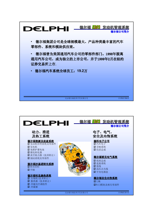
德尔福
发动机管理系统
德尔福公司简介
德尔福在亚太地区拥有优秀的发动机管理系统工程开发和工程应用技术人员,可为本地区客户提供全面的 发动机管理系统和零部件技术支持
中华人CH民IN共A 和国
•成套发动机管理系统开发标定工程团队 -北京工程开发应用技术中心 •发动机管理系统零部件工程开发及应用技术中心 -上海外高桥 -北京客户服务中心及零部件制造企业
MAX2870中文规格书

PARAMETER
CONDITIONS
REFERENCE OSCILLATOR INPUT (REF_IN)
REF_IN Input Frequency Range
REF_IN Input Sensitivity
REF_IN Input Capacitance
REF_IN Input Current
CONDITIONS
CP[3:0] = 1111, RSET = 5.1kI CP[3:0] = 0000, RSET = 5.1kI
With output dividers (1/2/4/8/16/32/64/128)
Open loop Open loop into 2:1 VSWR Fundamental VCO output Fundamental VCO output VCO output divided-by-2 VCO output divided-by-2
定购信息在数据资料的最后给出。 典型应用电路在数据手资料的最后给出。
相关型号以及配合该器件使用的推荐产品,请参见:china.maximintegrated. com/MAX2870.related。
功能框图
MAX2870
REF_IN
CLK DATA
LE
MUX
R COUNTER
X2
SPI AND REGISTERS
Both channels enabled, maximum output power
Total, including RFOUT, both channel (Note 3)
Each output divide-by-2 ICCVCO + ICCRF (Note 3) Low-power sleep mode
IR选型指南
600V 应用系统,输出推/拉电流为 200/420mA
型号
电路
VCC 范围
IR2130 3-Phase Bridge Driver IR2131 3HI/3LO MOS Driver IR2132 3-Phase Bridge Driver 10-25V with UVLO IR2133 3-Phase Bridge Driver IR2135 3-Phase Bridge Driver
Ton/Toff
VIH/VIL
Vitrip+ UVCC/BS+/CCBS-
IR2136
IR21362
12-25V with UVLO
IR21363
IR21365
IR21366 IR21367
12-20V with UVLO
IR21368
10V/20V
___ __ 400ns/380ns 2.7V/1.7V 0.46V
电路
IC@25°C IC@100°C VCE(on)@25°C
Co-Pack 12A
6.8A
2.1V
Co-Pack 12A
6.8A
2.1V
Co-Pack 13A
7A
1.8V
Co-Pack 17A
9A
1.8V
Co-Pack 22A
12A
1.8V
Co-Pack 31A
15A
1.8V
Isolated TO-220 Full-Pak
Co-Pack 9A
6A
1.8V
Isolated TO-220 Full-Pak
Co-Pack 12A
Hale Waihona Puke 8A1.8VIsolated TO-220 Full-Pak
MAXIM MAX9400 9402 9403 9405 说明书

General DescriptionThe MAX9400/MAX9402/MAX9403/MAX9405 are extremely fast, low-skew quad LVECL/ECL or LVPECL/PECL buffer/receivers designed for high-speed data and clock driver applications. These devices feature an ultra-low propagation delay of 335ps and channel-to-channel skew of 16ps in asynchronous mode with 86mA supply current.The four channels can be operated synchronously with an external clock, or in asynchronous mode determined by the state of the SEL input. An enable input provides the ability to force all the outputs to a differential low state.A variety of input and output terminations are offered for maximum design flexibility. The MAX9400 has open inputs and open emitter outputs. The MAX9402 has open inputs and 50Ωseries outputs. The MAX9403 has 100Ωdifferential input impedance and open emitter outputs. The MAX9405 has 100Ωdifferential input impedance and 50Ωseries outputs.These devices operate with a supply voltage of (V CC -V EE ) = 2.375V to 5.5V, and are specified for operation from -40°C to +85°C. These devices are offered in space-saving 32-pin 5mm ✕5mm TQFP and 32-lead 5mm ✕5mm QFN packages.ApplicationsData and Clock Driver and BufferCentral Office Backplane Clock Distribution DSLAM Backplane Base Station ATEFeatures♦400mV Differential Output at 3.0GHz Data Rate ♦335ps Propagation Delay in Asynchronous Mode ♦8ps Channel-to-Channel Skew in Synchronous Mode ♦Integrated 50ΩOutputs (MAX9402/MAX9405)♦Integrated 100ΩInputs (MAX9403/MAX9405)♦Synchronous/Asynchronous OperationMAX9400/MAX9402/MAX9403/MAX9405Quad Differential LVECL/LVPECLBuffer/Receivers________________________________________________________________Maxim Integrated Products1Ordering InformationPin Configurations19-2223; Rev 2; 1/05For pricing, delivery, and ordering information,please contact Maxim/Dallas Direct!at 1-888-629-4642, or visit Maxim’s website at .Functional Diagram appears at end of data sheet.M A X 9400/M A X 9402/M A X 9403/M A X 9405Quad Differential LVECL/LVPECL Buffer/ReceiversABSOLUTE MAXIMUM RATINGSDC ELECTRICAL CHARACTERISTICS(V CC - V EE = 2.375V to 5.5V, MAX9400/MAX9403 outputs terminated with 50Ω±1% to V CC - 2.0V. Typical values are at V CC - V EE =Stresses beyond those listed under “Absolute Maximum Ratings” may cause permanent damage to the device. These are stress ratings only, and functional operation of the device at these or any other conditions beyond those indicated in the operational sections of the specifications is not implied. Exposure to absolute maximum rating conditions for extended periods may affect device reliability.V CC to V EE ................................................................-0.3V to +6V Inputs to V EE ...............................................-0.3V to (V CC + 0.3V)Differential Input Voltage .......................................................±3V Continuous Output Current.................................................50mA Surge Output Current........................................................100mA Continuous Power Dissipation (T A = +70°C)32-Pin 5mm x 5mm TQFP(derate 9.5mW/°C above +70°C).................................761mW 32-Lead 5mm x 5mm QFN(derate 21.3mW/°C above +70°C)...................................1.7W Junction-to-Ambient Thermal Resistance in Still Air32-Pin 5mm x 5mm TQFP........................................+105°C/W 32-Lead 5mm x 5mm QFN........................................+47°C/WJunction-to-Ambient Thermal Resistance with 500LFPM Airflow32-Pin 5mm x 5mm TQFP.........................................+73°C/W Junction-to-Case Thermal Resistance32-Pin 5mm x 5mm TQFP.........................................+25°C/W 32-Lead 5mm x 5mm QFN.........................................+2°C/W Operating Temperature Range ...........................-40°C to +85°C Junction Temperature......................................................+150°C Storage Temperature Range.............................-65°C to +150°C ESD ProtectionHuman Body Model (Inputs and Outputs)........................2kV Soldering Temperature (10s)...........................................+300°CAC ELECTRICAL CHARACTERISTICSMAX9400/MAX9402/MAX9403/MAX9405Quad Differential LVECL/LVPECL Buffer/Receivers (V CC- V EE= 2.375V to 5.5V, outputs terminated with 50Ω±1% to V CC- 2.0V, enabled, CLK = 3.2GHz, f IN= 1.6GHz, input transitiontime = 125ps (20% to 80%), V IHD= V EE+ 1.2V to V CC, V ILD= V EE to V CC- 0.2V, V IHD- V ILD= 0.2V to smaller of |V CC- V EE| or 3V,Note 1:Measurements are made with the device in thermal equilibrium.Note 2:Current into a pin is defined as positive. Current out of a pin is defined as negative.Note 3:DC parameters are production tested at +25°C. DC limits are guaranteed by design and characterization over the full oper-ating temperature range.Note 4:Guaranteed by design and characterization. Limits are set to ±6 sigma.Note 5:Measured between outputs of the same part at the signal crossing points for a same-edge transition.Note 6:Device jitter added to the input signal._______________________________________________________________________________________3M A X 9400/M A X 9402/M A X 9403/M A X 9405Quad Differential LVECL/LVPECL Buffer/Receivers 4_______________________________________________________________________________________Typical Operating Characteristics(V CC - V EE = 3.3V, MAX9400, outputs terminated with 50Ω±1% to V CC - 2.0V, enabled, SEL = high, CLK = 2.0GHz, f IN = 1.0GHz,input transition time = 125ps (20% to 80%), V IHD = V CC - 1.0V, V ILD = V CC - 1.5V, T A = +25°C, unless otherwise noted.)707585809095-4010-15356085SUPPLY CURRENT (I EE )vs. TEMPERATUREM A X 9400 t o c 01TEMPERATURE (°C)S U P P L Y C U R R E N T (m A )020060040080010000100050015002000250030003500OUTPUT AMPLITUDE (V OH - V OL )vs. IN_ FREQUENCYM A X 9400 t o c 02IN_ FREQUENCY (MHz)O U T P U T A M P L I T U D E (m V )10090807060-4010-15356085OUTPUT RISE/FALL vs. TEMPERATUREM A X 9400 t o c 03TEMPERATURE (°C)O U T P U T R I S E /F A L L T I M E (p s )t Rt F325335330345340350355-4085IN-TO-OUT PROPAGATION DELAYvs. TEMPERATURETEMPERATURE (°C)P R O P A G A T I O N D E L A Y (p s )10-153560520500480460440-4010-15356085CLK-TO-OUT PROPAGATION DELAYvs. TEMPERATURETEMPERATURE (°C)P R O P A G A T I O N D E L A Y (p s )Pin DescriptionMAX9400/MAX9402/MAX9403/MAX9405Quad Differential LVECL/LVPECL Buffer/ReceiversM A X 9400/M A X 9402/M A X 9403/M A X 9405Detailed DescriptionThe MAX9400/MAX9402/MAX9403/MAX9405 are extremely fast, low-skew quad LVECL/ECL or LVPECL/PECL buffer/receivers designed for high-speed data and clock driver applications. The devices feature an ultra-low propagation delay of 335ps and channel-to-channel skew of 16ps in asynchronous mode with an 86mA supply current.The four channels can be operated synchronously with an external clock, or in asynchronous mode, determined by the state of the SEL input. An enable input provides the ability to force all the outputs to a differential low state.A variety of input and output terminations are offered for maximum design flexibility. The MAX9400 has open inputs and open-emitter outputs. The MAX9402 has open inputs and 50Ωseries outputs. The MAX9403 has 100Ωdifferential input impedance and open-emitter outputs. The MAX9405 has 100Ωdifferential input impedance and 50Ωseries outputs.Supply VoltageThe MAX9400/MAX9402/MAX9403/MAX9405 are de-signed for operation with a single supply. Using a single negative supply of V EE = -2.375V to -5.5V (V CC = ground)yields LVECL/ECL-compatible input and output ing a single positive supply of V CC = 2.375V to 5.5V (V EE = ground) yields LVPECL/PECL input and output levels.Data InputsThe MAX9400/MAX9402 have open inputs and require external termination. The MAX9403/MAX9405 have inte-grated 100Ωdifferential input termination resistors from IN_ to IN_,reducing external component count.OutputsThe MAX9402/MAX9405 have internal 50Ωseries out-put termination resistors and 8mA internal pulldown current sources. Using integrated resistors reduces external component count.The MAX9400/MAX9403 have open-emitter outputs. An external termination is required. See the Output Termination section.EnableSetting EN = high and EN = low enables the device.Setting EN = low and EN = high forces the outputs to a differential low, and all changes on CLK, SEL, and IN_are ignored.Asynchronous OperationSetting SEL = high and SEL = low enables the four channels to operate independently as buffer/receivers.The CLK signal is ignored in this mode. In asynchro-nous mode, the CLK signal should be set to either a logic low or high state to minimize noise coupling.Synchronous OperationSetting SEL = low and SEL = high enables all four channels to operate in synchronous mode. In this mode, buffered inputs are clocked into flip-flops simul-taneously on the rising edge of the differential clock input (CLK and CLK ).Differential Signal Input LimitThe maximum signal magnitude of the differential inputs is V CC - V EE or 3V, whichever is less.Applications InformationInput BiasUnused inputs should be biased or driven as shown in Figure 5. This avoids noise coupling that might cause toggling at the unused outputs.Output TerminationTerminate open-emitter outputs (MAX9400/MAX9403)through 50Ωto V CC - 2V or use an equivalent Thevenin termination. Terminate both outputs and use identical termination on each for the lowest output-to-output skew. When a single-ended signal is taken from a dif-ferential output, terminate both outputs. For example, if OUT_ is used as a single-ended output, terminate both OUT_ and OUT_.Ensure that the output currents do not exceed the cur-rent limits as specified in the Absolute Ma ximum Ratings table. Under all operating conditions, the device’s total thermal limits should be observed.Power-Supply BypassingAdequate power-supply bypassing is necessary to maximize the performance and noise immunity. Bypass V CC to V EE with high-frequency surface-mount ceramic 0.1µF and 0.01µF capacitors as close to the device as possible with the 0.01µF capacitor closest to the device pins. Use multiple bypass vias for connection to mini-mize inductance.Circuit Board TracesInput and output trace characteristics affect the perfor-mance of the MAX9400/MAX9402/MAX9403/MAX9405.Connect each of the inputs and outputs to a 50Ωchar-acteristic impedance trace. Avoid discontinuities in dif-ferential impedance and maximize common-mode noise immunity by maintaining the distance between differential traces and avoid sharp corners. Minimize the number of vias to prevent impedance discontinu-ities. Reduce reflections by maintaining the 50Ωchar-Quad Differential LVECL/LVPECL Buffer/Receivers 6_______________________________________________________________________________________acteristic impedance through connectors and across cables. Minimize skew by matching the electrical length of the traces.Chip InformationTRANSISTOR COUNT: 713PROCESS: BipolarMAX9400/MAX9402/MAX9403/MAX9405Quad Differential LVECL/LVPECLBuffer/Receivers_______________________________________________________________________________________7Figure 1. Input and Output Voltage DefinitionsFigure 2. Input and Output ConfigurationsM A X 9400/M A X 9402/M A X 9403/M A X 9405Quad Differential LVECL/LVPECL Buffer/Receivers 8_______________________________________________________________________________________Figure 4. CLK-to-OUT Propagation Delay Timing DiagramMAX9400/MAX9402/MAX9403/MAX9405Quad Differential LVECL/LVPECLBuffer/Receivers_______________________________________________________________________________________9Figure 5. Input Bias Circuits for Unused InputsPin Configurations (continued)M A X 9400/M A X 9402/M A X 9403/M A X 9405Quad Differential LVECL/LVPECL Buffer/Receivers 10______________________________________________________________________________________Functional DiagramPackage InformationMAX9400/MAX9402/MAX9403/MAX9405Quad Differential LVECL/LVPECL Buffer/ReceiversMA X 9400/M A X 9402/M A X 9403/M A X 9405Quad Differential LVECL/LVPECL Buffer/Receivers12______________________________________________________________________________________Package Information (continued)(The package drawing(s) in this data sheet may not reflect the most current specifications. For the latest package outline information,go to /packages .MAX9400/MAX9402/MAX9403/MAX9405Quad Differential LVECL/LVPECL Buffer/ReceiversMa xim ca nnot a ssume responsibility for use of a ny circuitry other tha n circuitry entirely embodied in a Ma xim product. No circuit pa tent licenses a re implied. Maxim reserves the right to change the circuitry and specifications without notice at any time.Maxim Integrated Products, 120 San Gabriel Drive, Sunnyvale, CA 94086 408-737-7600 ____________________13©2005 Maxim Integrated Productsis a registered trademark of Maxim Integrated Products, Inc.Package Information (continued)(The package drawing(s) in this data sheet may not reflect the most current specifications. For the latest package outline information,go to /packages .。
MAX232中文资料.pdf
________________________________MAX220–MAX249 / Lj EIA/TIA-232E V.28/V.24 Lj ±12V ăӼ Lj 5μW ăMAX225ĂMAX233ĂMAX235 MAX245/MAX246/MAX247ԥ ԩ Lj ғ ă________________________________ӯRS-232 RS-232_______________________♦ Ă ESD үMAX3222E/MAX3232E/MAX3237E/MAX3241E/MAX3246E ǖ+3.0V +5.5V Ă Ă 1Mbps Ă 0.1μFRS-232 (MAX3246E UCSP TM )♦ ӊMAX221E ǖ±15kV ESD ү Ă+5V Ă1μA ĂAutoShutdown TM RS-232MAX220–MAX249+5V Ă RS-232/_____________________________________________________________________ ӹ19-4323; Rev 15; 1/06_____________________________ࢾ৪ቧᇦ)ኚ*Ᏼၫᓾ೯ࡼᔢઁ߲ă*ൡຢਖৃLj༿ᎧޣೊᇹăAutoShutdown UCSP Maxim Integrated Products, Inc. Ӷă۾ᆪဵNbyjnᑵါ፞ᆪᓾ೯ࡼፉᆪLjNbyjnݙ࣪डፉᒦࡀᏴࡼތፊᎅࠥޘညࡼࡇᇙঌᐊă༿ᓖፀፉᆪᒦభถࡀᏴᆪᔊᔝᒅडፉࡇᇙLjྙኊཀྵཱྀྀੜࠤᎫࡼᓰཀྵቶLj༿ݬఠNbyjnᄋࡼ፞ᆪۈᓾ೯ăჃནॅዹອਜ਼ᔢቤۈࡼၫᓾ೯Lj༿षᆰNbyjnࡼᓍǖxxx/nbyjn.jd/dpn/doăM A X 220–M A X 249+5V Ă RS-232 / 2_______________________________________________________________________________________ABSOLUTE MAXIMUM RATINGS—MAX220/222/232A/233A/242/243ELECTRICAL CHARACTERISTICS—MAX220/222/232A/233A/242/243(V CC = +5V ±10%, C1–C4 = 0.1μF‚ MAX220, C1 = 0.047μF, C2–C4 = 0.33μF, T A = T MIN to T MAX ‚ unless otherwise noted.)Note 1:For the MAX220, V+ and V- can have a maximum magnitude of 7V, but their absolute difference cannot exceed 13V.Note 2:Input voltage measured with T OUT in high-impedance state, SHDN or V CC = 0V.Note 3:Maximum reflow temperature for the MAX233A is +225°C.Stresses beyond those listed under “Absolute Maximum Ratings” may cause permanent damage to the device. These are stress ratings only, and functional operation of the device at these or any other conditions beyond those indicated in the operational sections of the specifications is not implied. Exposure to absolute maximum rating conditions for extended periods may affect device reliability.Supply Voltage (V CC )...............................................-0.3V to +6V V+ (Note 1)..................................................(V CC - 0.3V) to +14V V- (Note 1).............................................................+0.3V to +14V Input VoltagesT IN ..............................................................-0.3V to (V CC - 0.3V)R IN (Except MAX220)........................................................±30V R IN (MAX220).....................................................................±25V T OUT (Except MAX220) (Note 2).......................................±15V T OUT (MAX220)...............................................................±13.2V Output VoltagesT OUT ...................................................................................±15V R OUT .........................................................-0.3V to (V CC + 0.3V)Driver/Receiver Output Short Circuited to GND.........Continuous Continuous Power Dissipation (T A = +70°C)16-Pin Plastic DIP (derate 10.53mW/°C above +70°C).842mW18-Pin Plastic DIP (derate 11.11mW/°C above +70°C)..889mW 20-Pin Plastic DIP (derate 8.00mW/°C above +70°C)..440mW 16-Pin Narrow SO (derate 8.70mW/°C above +70°C)...696mW 16-Pin Wide SO (derate 9.52mW/°C above +70°C)......762mW 18-Pin Wide SO (derate 9.52mW/°C above +70°C)......762mW 20-Pin Wide SO (derate 10.00mW/°C above +70°C)....800mW 20-Pin SSOP (derate 8.00mW/°C above +70°C)..........640mW 16-Pin CERDIP (derate 10.00mW/°C above +70°C).....800mW 18-Pin CERDIP (derate 10.53mW/°C above +70°C).....842mW Operating Temperature RangesMAX2_ _AC_ _, MAX2_ _C_ _.............................0°C to +70°C MAX2_ _AE_ _, MAX2_ _E_ _..........................-40°C to +85°C MAX2_ _AM_ _, MAX2_ _M_ _.......................-55°C to +125°C Storage Temperature Range.............................-65°C to +160°C Lead Temperature (soldering, 10s) (Note 3)...................+300°CMAX220–MAX249+5V Ă RS-232/_______________________________________________________________________________________3OUT IN ELECTRICAL CHARACTERISTICS—MAX220/222/232A/233A/242/243 (continued)(V CC = +5V ±10%, C1–C4 = 0.1μF‚ MAX220, C1 = 0.047μF, C2–C4 = 0.33μF, T A = T MIN to T MAX ‚ unless otherwise noted.)M A X 220–M A X 249+5V Ă RS-232 / 4_______________________________________________________________________________________________________________________________________________________MAX220/MAX222/MAX232A/MAX233A/MAX242/MAX243108-1051525OUTPUT VOLTAGE vs. LOAD CURRENT-4-6-8-2642LOAD CURRENT (mA)O U T P U T V O L T A G E (V )1002011104104060AVAILABLE OUTPUT CURRENTvs. DATA RATE65798DATA RATE (kb/s)O U T P U T C U R R E N T (m A )203050+10V-10VMAX222/MAX242ON-TIME EXITING SHUTDOWN+5V +5V 0V0V 500μs/div V +, V - V O L T A G E (V )ELECTRICAL CHARACTERISTICS—MAX220/222/232A/233A/242/243 (continued)(V CC = +5V ±10%, C1–C4 = 0.1μF‚ MAX220, C1 = 0.047μF, C2–C4 = 0.33μF, T A = T MIN to T MAX ‚ unless otherwise noted.)MAX220–MAX249+5V Ă RS-232/_______________________________________________________________________________________5V CC ...........................................................................-0.3V to +6V V+................................................................(V CC - 0.3V) to +14V V-............................................................................+0.3V to -14V Input VoltagesT IN ............................................................-0.3V to (V CC + 0.3V)R IN ......................................................................................±30V Output VoltagesT OUT ...................................................(V+ + 0.3V) to (V- - 0.3V)R OUT .........................................................-0.3V to (V CC + 0.3V)Short-Circuit Duration, T OUT ......................................Continuous Continuous Power Dissipation (T A = +70°C)14-Pin Plastic DIP (derate 10.00mW/°C above +70°C)....800mW 16-Pin Plastic DIP (derate 10.53mW/°C above +70°C)....842mW 20-Pin Plastic DIP (derate 11.11mW/°C above +70°C)....889mW 24-Pin Narrow Plastic DIP(derate 13.33mW/°C above +70°C)..........1.07W24-Pin Plastic DIP (derate 9.09mW/°C above +70°C)......500mW 16-Pin Wide SO (derate 9.52mW/°C above +70°C).........762mW20-Pin Wide SO (derate 10.00mW/°C above +70°C).......800mW 24-Pin Wide SO (derate 11.76mW/°C above +70°C).......941mW 28-Pin Wide SO (derate 12.50mW/°C above +70°C) .............1W 44-Pin Plastic FP (derate 11.11mW/°C above +70°C).....889mW 14-Pin CERDIP (derate 9.09mW/°C above +70°C)..........727mW 16-Pin CERDIP (derate 10.00mW/°C above +70°C)........800mW 20-Pin CERDIP (derate 11.11mW/°C above +70°C)........889mW 24-Pin Narrow CERDIP(derate 12.50mW/°C above +70°C)..............1W24-Pin Sidebraze (derate 20.0mW/°C above +70°C)..........1.6W 28-Pin SSOP (derate 9.52mW/°C above +70°C).............762mW Operating Temperature RangesMAX2 _ _ C _ _......................................................0°C to +70°C MAX2 _ _ E _ _...................................................-40°C to +85°C MAX2 _ _ M _ _................................................-55°C to +125°C Storage Temperature Range.............................-65°C to +160°C Lead Temperature (soldering, 10s) (Note 4)...................+300°CABSOLUTE MAXIMUM RATINGS—MAX223/MAX230–MAX241ELECTRICAL CHARACTERISTICS—MAX223/MAX230–MAX241(MAX223/230/232/234/236/237/238/240/241, V CC = +5V ±10%; MAX233/MAX235, V CC = 5V ±5%‚ C1–C4 = 1.0μF; MAX231/MAX239,V CC = 5V ±10%; V+ = 7.5V to 13.2V; T A = T MIN to T MAX ; unless otherwise noted.)Stresses beyond those listed under “Absolute Maximum Ratings” may cause permanent damage to the device. These are stress ratings only, and functional operation of the device at these or any other conditions beyond those indicated in the operational sections of the specifications is not implied. Exposure to absolute maximum rating conditions for extended periods may affect device reliability.Note 4:Maximum reflow temperature for the MAX233/MAX235 is +225°C.M A X 220–M A X 249+5V Ă RS-232 / 6_______________________________________________________________________________________ELECTRICAL CHARACTERISTICS—MAX223/MAX230–MAX241 (continued)(MAX223/230/232/234/236/237/238/240/241, V CC = +5V ±10%; MAX233/MAX235, V CC = 5V ±5%‚ C1–C4 = 1.0μF; MAX231/MAX239,V CC = 5V ±10%; V+ = 7.5V to 13.2V; T A = T MIN to T MAX ; unless otherwise noted.)MAX220–MAX249+5V Ă RS-232/_______________________________________________________________________________________7_______________________________________________________________MAX223/MAX230–MAX2418.56.54.55.5TRANSMITTER OUTPUT VOLTAGE (V OH ) vs. V CC7.08.0V CC (V)V O H (V )5.07.57.46.02500TRANSMITTER OUTPUT VOLTAGE (V OH )vs. LOAD CAPACITANCE AT DIFFERENT DATA RATES6.46.27.27.0LOAD CAPACITANCE (pF)V O H (V )1500100050020006.86.612.04.02500TRANSMITTER SLEW RATE vs. LOAD CAPACITANCE6.05.011.09.010.0LOAD CAPACITANCE (pF)S L E W R A T E (V /μs )1500100050020008.07.0-6.0-9.04.55.5TRANSMITTER OUTPUT VOLTAGE (V OL ) vs. V CC-8.0-8.5-6.5-7.0V CC (V)V O L (V )5.0-7.5-6.0-7.62500TRANSMITTER OUTPUT VOLTAGE (V OL )vs. LOAD CAPACITANCE AT DIFFERENT DATA RATES-7.0-7.2-7.4-6.2-6.4LOAD CAPACITANCE (pF)V O L (V )150010005002000-6.6-6.810-105101520253035404550TRANSMITTER OUTPUT VOLTAGE (V+, V-)vs. LOAD CURRENT-2-6-4-886CURRENT (mA)V +, V - (V )420*SHUTDOWN POLARITY IS REVERSED FOR NON MAX241 PARTSV+, V- WHEN EXITING SHUTDOWN(1μF CAPACITORS)MAX220-13SHDN*V-O V+500ms/divM A X 220–M A X 249+5V Ă RS-232 / 8_______________________________________________________________________________________ABSOLUTE MAXIMUM RATINGS—MAX225/MAX244–MAX249ELECTRICAL CHARACTERISTICS—MAX225/MAX244–MAX249(MAX225, V CC = 5.0V ±5%; MAX244–MAX249, V CC = +5.0V ±10%, external capacitors C1–C4 = 1μF; T A = T MIN to T MAX ; unless oth-erwise noted.)Stresses beyond those listed under “Absolute Maximum Ratings” may cause permanent damage to the device. These are stress ratings only, and functional operation of the device at these or any other conditions beyond those indicated in the operational sections of the specifications is not implied. Exposure to absolute maximum rating conditions for extended periods may affect device reliability.Supply Voltage (V CC )...............................................-0.3V to +6V Input VoltagesT IN ‚ ENA , ENB , ENR , ENT , ENRA ,ENRB , ENTA , ENTB ..................................-0.3V to (V CC + 0.3V)R IN .....................................................................................±25V T OUT (Note 5).....................................................................±15V R OUT ........................................................-0.3V to (V CC + 0.3V)Short Circuit (one output at a time)T OUT to GND............................................................Continuous R OUT to GND............................................................ContinuousContinuous Power Dissipation (T A = +70°C)28-Pin Wide SO (derate 12.50mW/°C above +70°C).............1W 40-Pin Plastic DIP (derate 11.11mW/°C above +70°C)...611mW 44-Pin PLCC (derate 13.33mW/°C above +70°C)...........1.07W Operating Temperature RangesMAX225C_ _, MAX24_C_ _ ..................................0°C to +70°C MAX225E_ _, MAX24_E_ _ ...............................-40°C to +85°C Storage Temperature Range.............................-65°C to +160°C Lead Temperature (soldering,10s) (Note 6)....................+300°CNote 5:Input voltage measured with transmitter output in a high-impedance state, shutdown, or V CC = 0V.Note 6:Maximum reflow temperature for the MAX225/MAX245/MAX246/MAX247 is +225°C.MAX220–MAX249+5V Ă RS-232/_______________________________________________________________________________________9Note 7:The 300Ωminimum specification complies with EIA/TIA-232E, but the actual resistance when in shutdown mode or V CC =0V is 10M Ωas is implied by the leakage specification.ELECTRICAL CHARACTERISTICS—MAX225/MAX244–MAX249 (continued)(MAX225, V CC = 5.0V ±5%; MAX244–MAX249, V CC = +5.0V ±10%, external capacitors C1–C4 = 1μF; T A = T MIN to T MAX ; unless oth-erwise noted.)M A X 220–M A X 249+5V Ă RS-232 / 10_____________________________________________________________________________________________________________________________________________________MAX225/MAX244–MAX24918212345TRANSMITTER SLEW RATE vs. LOAD CAPACITANCE86416LOAD CAPACITANCE (nF)T R A N S M I T T E R S L E W R A T E (V /μs )14121010-105101520253035OUTPUT VOLTAGEvs. LOAD CURRENT FOR V+ AND V--2-4-6-88LOAD CURRENT (mA)O U T P U T V O L T A G E (V )64209.05.012345TRANSMITTER OUTPUT VOLTAGE (V+, V-)vs. LOAD CAPACITANCE AT DIFFERENT DATA RATES6.05.58.5LOAD CAPACITANCE (nF)V +, V (V )8.07.57.06.5MAX220–MAX249+5V RS-232/1. 2.3. 4.M A X 220–M A X 249+5V RS-232 / ENT ENR OPERATION STATUS TRANSMITTERSRECEIVERS00Normal Operation All Active All Active 01Normal Operation All Active All 3-State10Shutdown All 3-State All Low-Power Receive Mode 11ShutdownAll 3-StateAll 3-Stateӹ1a. MAX245ENT ENR OPERATION STATUS TRANSMITTERS RECEIVERSTA1–TA4TB1–TB4RA1–RA5RB1–RB500Normal Operation All Active All Active All Active All Active 01Normal Operation All Active All Active RA1–RA4 3-State,RA5 Active RB1–RB4 3-State,RB5 Active 1ShutdownAll 3-StateAll 3-StateAll Low-Power Receive Mode All Low-Power Receive Mode 11Shutdown All 3-State All 3-StateRA1–RA4 3-State,RA5 Low-Power Receive ModeRB1–RB4 3-State,RB5 Low-Power Receive Modeӹ1b. MAX245ӹ1c. MAX246ENA ENB OPERATION STATUS TRANSMITTERS RECEIVERSTA1–TA4TB1–TB4RA1–RA5RB1–RB500Normal Operation All Active All Active All Active All Active 01Normal Operation All Active All 3-State All Active RB1–RB4 3-State,RB5 Active 1ShutdownAll 3-StateAll ActiveRA1–RA4 3-State,RA5 Active All Active 11Shutdown All 3-State All 3-StateRA1–RA4 3-State,RA5 Low-Power Receive ModeRB1–RB4 3-State,RA5 Low-Power Receive ModeMAX220–MAX249+5V RS-232/M A X 220–M A X 249____________________________MAX220–MAX249Ҫ 4 ԩ ǖ ӏDC-DC ĂRS-232 ĂRS-232 Lj ăӏMAX220–MAX249 ԩ ӏLj +5V ±10V ( )Lj RS-232 ă C1 +5V ӂLj V+ C3 +10V Ǘ C2 +10V V- C4 -10V ă+10V (V+) -10V (V-) Lj ԩ (Ը ԩ )Ǘ MAX225 MAX245–MAX247 Lj ԥ ăV+ V- Lj ă V+ĂV- ԩ Lj ԥ V+ĂV- EIA/TIA-232E ±5V ăMAX222ĂMAX225ĂMAX230ĂMAX235ĂMAX236ĂMAX240ĂMAX241 MAX245–MAX249 Lj Ө V+ V- ԩ ă LjV- 0V LjV+ +5V ă +10V ԩ V+ ( ԥ ԩ ӏ դ +10V) Lj ԥ Ѡ C1LjԌ Ӥ SHDN V CC Lj V+Ӈ ԩ V CC ăRS-232Ӷ 5kΩ RS-232 LjԌ V CC =+5V Lj ҈ ±8V ă ҈ ү EIA/TIA-232E V.28 Lj ±5V Lj Ҫ 3kΩ ĂV CC = +4.5V ă (V +-1.3V) (V- +0.5V)ăTTL CMOS ă ԥ Lj Ă V CC 400kΩ (MAX220 )ă Lj ă Ӈ Lj ԩ ի 12μA ă Ă ӇLj ӡLjԌ Lj ի Ѡ( 25μA)ă Ӈ ±15V ă Lj ի 8μA ăMAX220ԥ ӄ ԩ Lj ԥ Lj GND V CC ăMAX239 Lj MAX223ĂMAX225ĂMAX235ĂMAX236ĂMAX240 MAX241 ӄ ăӹ2 ă( MAX225/MAX235/MAX236/MAX239–MAX241)Lj TTL/CMOS Ă Ǘ Lj Lj ăLj Ӈ ӡLj 1μA Lj Ӈ ă 1μA Lj ӯ Ӈ 0V (V CC +6V)ă -0.5V Lj Lj 1kΩ ă Ӈ V CC +6V Lj 1kΩ ă҈ 30V/μs Lj EIA/TIA-232E V.28 ă҈ ǖ 24V/μs Lj3Ω 2500pF 10V/μs ăRS-232EIA/TIA-232E V.28 3V 0Lj Lj ă 0.8V 2.4V Lj TTL Lj EIA/TIA-232E V.28 ă±25V LjԌ Ӷ 5kΩ ă V.28 EIA/TIA-232E ă+5V RS-232 /ӹMAX220–MAX249+5V RS-232/0.5V LjԌ ү0.2V ă Lj Ӱ դ ӰLj ă 600ns Lj ҈ ăMAX223ĂMAX242 MAX245–MAX249 Lj IC Lj ă ի ă Lj Lj ӄ Ă ă Ճ ă—MAX243MAX243 MAX232A Lj Ӽ RS-232 ү ă CTS RTS Ӈ Lj ԥ ăԥӤ ԥ ԥ ӄăү -0.8V Lj ԥ +1.4V ă Lj ԯӰ ă Lj 0Lj Đ đ ă իLjMAX243 (+1.4V ) (TD RD)Lj (DTR ĂDTS ĂCTS ĂRTS ) ăRS-232 դ Ѣ EIA/TIA-232E LjԳ ү ă Ӈ Ă Lj Ӱ ă IC ă Ө Lj Ӥ Ӈ Lj ă—MAX222–MAX242LjMAX222ĂMAX235ĂMAX236ĂMAX240 MAX241 Ӈ ă LjMAX223 MAX242 ү ă Lj ӰLj 2.5μs ă Lj CMOS ăMAX223 MAX242 ( MAX242 EN ĂMAX223 EN)Lj SHDN ( MAX241 SHDN) ă SHDN ( MAX241 SHDN ) ăMAX225 5 5 ǗMAX245 10 8 ă ă ENT Lj ӏ ӡԌ ă Lj 25μA Lj ү Lj ( )ăMAX225 5 ENR ăMAX245 8 ENR Lj (RA5 RB5) ү ă ENR LjRA1–RA4 RB1–RB4 ăMAX225 MAX245–MAX249 ăǖ ( ի )Ă ( ) ( ү )ă ă ǖ ( ի ) ( )ă Ӈ ă Ӈ Lj ă Lj ăM A X 220–M A X 249ӹ1a–1d ăMAX244 Lj Ҫ ӹ ăMAX246 10 8 Lj Lj Ӽ ՊăA Պ (ENA ) Lj 4 A Պ Ǘ LjB Պ (ENB ) 4 B Պ ă MAX245 Lj A Պ B Պ (RA5 RB5) ү ă A ՊĂB Պ Ӈ (ENA =ENB =+5V) Lj ăMAX247 9 8 Lj 4 ăENRA ĂENRB Lj Ӽ 4 ăENTA ĂENTB Lj Ӽ 4 ă 9 (RB5) ă ENTA ENTB ăMAX248 8 8 Lj 4 ăENRA ĂENRB Lj Ӽ 4ăENTA ĂENTB Lj Ӽ 4 ă ă ENTA ĂENTB Lj ăMAX249 10 6 Lj 4 ăENRA ĂENRB Lj Ӽ 5 ăENTA ĂENTB Lj Ӽ 3 ă ă ENTA ĂENTB Lj ă Ljү Lj 20kb/s ă____________________________5 25 ă LjV CC C1ĂC2 Lj ҈ ă+5V RS-232 /MAX220–MAX249+5V RS-232/5. MAX220/MAX232/MAX232A6. MAX222/MAX242M A X 220–M A X 249+5V RS-232 /7. MAX225MAX220–MAX249+5V RS-232/8. MAX223/MAX241M A X 220–M A X 249+5V RS-232 /9. MAX23010. MAX231MAX220–MAX249+5V RS-232/12. MAX23411. MAX233/MAX233AM A X 220–M A X 249+5V RS-232 /13. MAX235MAX220–MAX249+5V RS-232/14. MAX236M A X 220–M A X 249+5V RS-232 /15. MAX237MAX220–MAX249+5V RS-232/16. MAX238M A X 220–M A X 249+5V RS-232 /17. MAX239MAX220–MAX249+5V RS-232/18. MAX240M A X 220–M A X 249+5V RS-232 /19. MAX243MAX220–MAX249+5V RS-232/20. MAX244M A X 220–M A X 249+5V RS-232 /21. MAX245MAX220–MAX249+5V RS-232/______________________________________________________________________________________3122. MAX246M A X 220–M A X 249+5V RS-232 / 32______________________________________________________________________________________23. MAX247MAX220–MAX249+5V RS-232/______________________________________________________________________________________3324. MAX248M A X 220–M A X 249+5V RS-232 / 34______________________________________________________________________________________25. MAX249MAX220–MAX249+5V RS-232/______________________________________________________________________________________35_____________________________________________________________________ ( )*ൡຢਖৃLj༿ᎧޣೊᇹăM A X 220–M A X 249+5V RS-232 / _____________________________________________________________________ ( )*ൡຢਖৃLj༿Ꭷޣೊᇹă____________________________Lj Փ /packages ă_____________________________Rev 15 ǖ2–5Ă8Ă9Ă36ăNbyjnݙ࣪Nbyjnޘອጲᅪࡼྀੜ࢟വဧঌᐊLjጐݙᄋᓜಽభăNbyjnۣഔᏴྀੜဟମĂᎌྀੜᄰۨࡼ༄ᄋሆኀখޘອᓾ೯ਜ਼ਖৃࡼཚಽă36____________________Maxim Integrated Products, 120 San Gabriel Drive, Sunnyvale, CA 94086 408-737-7600©2006 Maxim Integrated ProductsNbyjn ဵNbyjn!Joufhsbufe!Qspevdut-!Jod/ࡼᓖݿܪăNbyjn ۱யێူࠀ۱ய9439ቧረᎆᑶܠ൩211194ॅ࢟જǖ911!921!1421࢟જǖ121.732262::ࠅᑞǖ121.732263::。
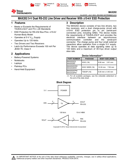
MAX3540

MAX3540——高度集成的低功耗一次变频电视调谐器1.芯片概述MAX3540完备的一次变频电视调谐器专为模拟/数字陆地接收机和数字机顶盒设计。
该电视调谐器采用+3.3V供电,功耗仅为760mW。
MAX3540能够将54MHz至860MHz带宽内的NTSC信号或A TSC信号转换成44MHz中频(IF)信号。
MAX3540包括可变增益低噪声放大器(LNA)、多频带跟踪滤波器、谐波抑制混频器、低噪声IF放大器、IF功率检测器以及可变增益IF放大器。
MAX3540还集成了单片VCO、谐振电路以及完整的频率合成器。
这款高集成度产品适用于低功耗板上调谐器应用,不存在二次变频调谐器方案中的成本及功耗等问题。
MAX3540工作在0°C至+85°C温度范围,采用48引脚、无铅倒装芯片(fcLGA)封装。
2.关键特性及应用范围1)关键特性•低功耗:+3.3V供电时功耗仅为760mW (典型值)•集成跟踪滤波器•符合A TSC A/74标准•40dB邻信道抑制比(ACPR)• 4.4dB (典型值)低噪声系数•微型、7mm x 7mm、fcLGA封装•符合256-QAM相位噪声的要求•IF过载检测器控制RF可变增益放大器•采用I²C兼容的2线串口2)应用•模拟/数字陆地接收机•电缆调制解调器•数字机顶盒•电视•V oIP网关3.引脚配置/典型应用电路4.使用注意事项使RF信号线尽可能短,以减小损耗和辐射;高频信号需采用阻抗受控的走线;应将裸焊盘焊接至电路板的地层。
关于布局布线的更多信息请参见MAX3540的数据资料。
MCP2515数据手册

1.3 SPI 协议模块
MCU通过SPI接口与该器件连接。使用标准的SPI读/写 指令以及专门的 SPI 命令来读 / 写所有的寄存器。
13
O 中断输出引脚
—
SCK
13
14
I SPI 接口的时钟输入引脚
—
SI
14
16
I SPI 接口的数据输入引脚
—
SO
15
17
O SPI 接口的数据输出引脚
—
CS
16
18
I SPI 接口的片选输入引脚
—
RESET
17
19
I 低电平有效的器件复位输入引脚
—
VDD
18
20
P 逻辑和 I/O 引脚的正电源
—
RXCAN TXCAN
CAN 协议
引擎
发送和接收缓冲器
验收屏蔽寄存器和 验收滤波器
SPI 接口
逻辑
CS SCK SI SO
SPI 总线
OSC1 OSC2 CLKOUT
时序 发生器
控制逻辑
控制 和 中断 寄存器
INT RX0BF RX1BF TX0RTS TX1RTS TX2RTS
RESET
2005 Microchip Technology Inc.
数据字段
协议 引擎
发送 <7:0>
移位 <14:0> { 发送 <5:0>,接收 <8:0>}
比较器
mb202i,max202芯片资料datasheet
5 V DINROUTDOUT RS-232RIN RS-232120 kb/s15 kV HBMCopyright © 2016,Texas Instruments IncorporatedProduct FolderSample &BuyTechnical Documents Tools &SoftwareSupport &CommunityAn IMPORTANT NOTICE at the end of this data sheet addresses availability,warranty,changes,use in safety-critical applications,intellectual property matters and other important disclaimers.PRODUCTION DATA.MAX202SLLS576F –JULY 2003–REVISED SETPEMBER 2016MAX2025-V Dual RS-232Line Driver and Receiver With ±15-kV ESD Protection1Features•Meets or Exceeds the Requirements of TIA/EIA-232-F and ITU v.28Standards•ESD Protection for RS-232Bus Pins:±15-kV Human-Body Model•Operates at 5-V V CC Supply •Operates Up to 120kbit/s•Two Drivers and Two Receivers•Latch-Up Performance Exceeds 100mA Per JESD 78,Class II2Applications•Battery-Powered Systems •Notebooks •Laptops•Palmtop PCs•Hand-Held Equipment3DescriptionThe MAX202device consists of two line drivers,two line receivers,and a dual charge-pump circuit with ±15-kV ESD protection pin to pin (serial-port connection pins,including GND).The device meets the requirements of TIA/EIA-232-F and provides the electrical interface between an asynchronous communication controller and the serial-port connector.The charge pump and four small external capacitors allow operation from a single 5-V supply.The device operates at data signaling rates up to 120kbit/s and a maximum of 30-V/µs driver output slew rate.Device Information (1)PART NUMBER PACKAGE BODY SIZE (NOM)MAX202CD MAX202ID SOIC (16)9.90mm ×3.91mm MAX202CDW MAX202IDW SOIC WIDE (16)10.30mm ×7.50mm MAX202CPW MAX202IPWTSSOP (16)5.00mm x 4.40mm(1)For all available packages,see the orderable addendum atthe end of the data sheet.Block Diagram2MAX202SLLS576F –JULY 2003–REVISED SETPEMBER 2016Product Folder Links:MAX202Submit Documentation FeedbackCopyright ©2003–2016,Texas Instruments IncorporatedTable of Contents1Features ..................................................................12Applications ...........................................................13Description .............................................................14Revision History .....................................................25Pin Configuration and Functions . (36)Specifications .........................................................46.1Absolute Maximum Ratings......................................46.2ESD Ratings..............................................................46.3Recommended Operating Conditions.......................46.4Thermal Information..................................................46.5Electrical Characteristics...........................................56.6Switching Characteristics..........................................56.7Typical Characteristics .............................................67Parameter Measurement Information ..................78Detailed Description . (8)8.1Overview...................................................................88.2Functional Block Diagram.. (8)8.3Feature Description...................................................88.4Device Functional Modes (8)9Application and Implementation (10)9.1Application Information............................................109.2Typical Application.. (10)10Power Supply Recommendations .....................1311Layout . (13)11.1Layout Guidelines ................................................1311.2Layout Example. (13)12Device and Documentation Support (14)12.1Receiving Notification of Documentation Updates 1412.2Community Resources..........................................1412.3Trademarks...........................................................1412.4Electrostatic Discharge Caution............................1412.5Glossary................................................................1413Mechanical,Packaging,and OrderableInformation (14)4Revision HistoryNOTE:Page numbers for previous revisions may differ from page numbers in the current version.Changes from Revision E (April 2007)to Revision F Page•Added ESD Ratings table,Feature Description section,Device Functional Modes ,Application and Implementation section,Power Supply Recommendations section,Layout section,Device and Documentation Support section,andMechanical,Packaging,and Orderable Information section..................................................................................................1•Removed the Ordering Information table;see POA at the end of the data sheet .................................................................1•Changed values in the Thermal Information table to align with JEDEC standards (4)C1+ V CC V+ GND C1± DOUT1C2+ RIN1C2± ROUT1V ± DIN1DOUT2 DIN2RIN2ROUT23MAX202SLLS576F –JULY 2003–REVISED SETPEMBER 2016Product Folder Links:MAX202Submit Documentation FeedbackCopyright ©2003–2016,Texas Instruments Incorporated 5Pin Configuration and FunctionsD,DW,or PW Package 16-Pin SOIC or TSSOPTop ViewPin FunctionsPINI/O DESCRIPTION 1C1+—Positive lead of C1capacitor2V+O Positive charge pump output for storage capacitor only 3C1–—Negative lead of C1capacitor 4C2+—Positive lead of C2capacitor 5C2–—Negative lead of C2capacitor6V–O Negative charge pump output for storage capacitor only 7DOUT2O RS-232line data output (to remote RS-232system)8RIN2I RS-232line data input (from remote RS-232system)9ROUT2O Logic data output (to UART)10DIN2I Logic data input (from UART)11DIN1I Logic data input (from UART)12ROUT1O Logic data output (to UART)13RIN1I RS-232line data input (from remote RS-232system)14DOUT1O RS-232line data output (to remote RS-232system)15GND —Ground16V CC—Supply voltage,connect to external 5-V power supply4MAX202SLLS576F –JULY 2003–REVISED SETPEMBER 2016Product Folder Links:MAX202Submit Documentation FeedbackCopyright ©2003–2016,Texas Instruments Incorporated(1)Stresses beyond those listed under Absolute Maximum Ratings may cause permanent damage to the device.These are stress ratings only,which do not imply functional operation of the device at these or any other conditions beyond those indicated under Recommended Operating Conditions .Exposure to absolute-maximum-rated conditions for extended periods may affect device reliability.(2)All voltages are with respect to network GND.6Specifications6.1Absolute Maximum Ratingsover operating free-air temperature range (unless otherwise noted)(1)MINMAX UNIT Supply voltage,V CC (2)–0.36V Positive charge pump voltage,V+(2)V CC –0.314V Negative charge pump voltage,V–(2)–140.3V Input voltage,V I Drivers –0.3V++0.3V Receivers ±30Output voltage,V ODrivers V––0.3V++0.3VReceivers–0.3V CC +0.3Short-circuit duration,D OUTContinuousOperating junction temperature,T J 150°C Storage temperature,T stg –65150°C (1)JEDEC document JEP155states that 500-V HBM allows safe manufacturing with a standard ESD control process.(2)JEDEC document JEP157states that 250-V CDM allows safe manufacturing with a standard ESD control process.6.2ESD RatingsVALUEUNITV (ESD)Electrostatic dischargeHuman-body model (HBM),per ANSI/ESDA/JEDEC JS-001(1)Pins 7,8,13,and 14±15000V All other pins±2000Charged-device model (CDM),per JEDEC specification JESD22-C101(2)±1500(1)Test conditions are C1–C4=0.1µF at V CC =5V ±0.5V.6.3Recommended Operating Conditionsover operating free-air temperature range (unless otherwise noted (1);see Figure 10)MINNOMMAX UNIT Supply voltage4.555.5V V IH Driver high-level input voltage (D IN )2V V IL Driver low-level input voltage (D IN )0.8V V I Driver input voltage (D IN )0 5.5V Receiver input voltage –3030T A Operating free-air temperatureMAX202C 070°CMAX202I–4085(1)For more information about traditional and new thermal metrics,see the Semiconductor and IC Package Thermal Metrics application report.6.4Thermal InformationTHERMAL METRIC (1)MAX202UNITD (SOIC)DW (SOIC)PW (TSSOP)16PINS 16PINS 16PINS R θJA Junction-to-ambient thermal resistance 76.276.8101°C/W R θJC(top)Junction-to-case (top)thermal resistance 36.839.636.4°C/W R θJB Junction-to-board thermal resistance 33.941.545.9°C/W ψJT Junction-to-top characterization parameter 6.712.6 2.7°C/W ψJB Junction-to-board characterization parameter33.640.945.3°C/W5MAX202SLLS576F –JULY 2003–REVISED SETPEMBER 2016Product Folder Links:MAX202Submit Documentation FeedbackCopyright ©2003–2016,Texas Instruments Incorporated (1)Test conditions are C1–C4=0.1µF at V CC =5V ±0.5V.(2)All typical values are at V CC =5V,and T A =25°C.(3)Short-circuit durations should be controlled to prevent exceeding the device absolute power-dissipation ratings,and not more than one output should be shorted at a time.6.5Electrical Characteristicsover recommended ranges of supply voltage and operating free-air temperature (unless otherwise noted;see Figure 10)(1)PARAMETERTEST CONDITIONSMINTYP (2)MAX UNIT I CC Supply currentNo load,V CC =5V815mADRIVER SECTIONV OH High-level output voltage D OUT at R L =3k Ωto GND,D IN =GND 59V V OL Low-level output voltage D OUT at R L =3k Ωto GND,D IN =V CC –5–9V I IH High-level input current V I =V CC 0200µA I IL Low-level input current V I at 0V0–200µA I OS (3)Short-circuit output current V CC =5.5V,V O =0V±10±60mA r O Output resistance V CC ,V+,and V–=0V,V O =±2V 300ΩRECEIVER SECTIONV OH High-level output voltage I OH =–1mA 3.5V CC –0.4V V OL Low-level output voltageI OL =1.6mA 0.4V V IT+Positive-going input threshold voltage V CC =5V,T A =25°C 1.7 2.4V V IT–Negative-going input threshold voltage V CC =5V,T A =25°C0.8 1.2V V hys Input hysteresis (V IT+–V IT–)0.20.51V r i Input resistanceV I =±3V to ±25V357k Ω(1)Test conditions are C1–C4=0.1µF at V CC =5V ±0.5V.(2)All typical values are at V CC =5V,and T A =25°C.(3)Pulse skew is defined as |t PLH –t PHL |of each channel of the same device.6.6Switching Characteristicsover recommended ranges of suply voltage and operating free-air temperature (unless otherwise noted;see Figure 10)(1)PARAMETERTEST CONDITIONSMINTYP (2)MAXUNITDRIVER SECTIONMaximum data rateC L =50pF to 1000pF,R L =3k Ωto 7k ΩoneD OUT switching,see Figure 6120kbit/s t PLH(D)Propagation delay time,low-to high-level output C L =2500pF,R L =3k Ω,all drivers loaded,see Figure 62µs t PHL(D)Propagation delay time,high-to low-level output C L =2500pF,R L =3k Ω,all drivers loaded,see Figure 62µs t sk(p)Pulse skew (3)C L =150to 2500pF,R L =3k Ωto 7k Ω,see Figure 7300ns SR(tr)Slew rate,transition regionC L =50to 1000pF,R L =3k Ωto 7k Ω,V CC =5V,see Figure 63630V/µsRECEIVER SECTION (SEE Figure 8)t PLH(R)Propagation delay time,low-to high-level output C L =150pF 0.510µs t PHL(R)Propagation delay time,high-to low-level output C L =150pF 0.510µs t sk(p)Pulse skew (3)C L =150pF300ns6MAX202SLLS576F –JULY 2003–REVISED SETPEMBER 2016Product Folder Links:MAX202Submit Documentation FeedbackCopyright ©2003–2016,Texas Instruments Incorporated6.7Typical Characteristicsat T A =25°C (unless otherwise noted)TEST CIRCUITVOLTAGE WAVEFORMS50%50%–3 V3 V1.5 V1.5 VOutputInputV OL V OHt PHL (R)t PLH (R)OutputA)TEST CIRCUITVOLTAGE WAVEFORMS0 V 3 VOutputInputV OLV OHt PLH (D)t PHL (D)50%50%1.5 V1.5 VRS-232OutputA)TEST CIRCUITVOLTAGE WAVEFORMS0 V3 VOutputInputV OLV OH t PLH (D)RS-232Outputt PHL (D)A)1.5 V1.5 V3 V –3 V3 V –3 VSR(tf) =6 Vt or t PHL(D PLH(D))7MAX202SLLS576F –JULY 2003–REVISED SETPEMBER 2016Product Folder Links:MAX202Submit Documentation FeedbackCopyright ©2003–2016,Texas Instruments Incorporated 7Parameter Measurement InformationA.C L includes probe and jig capacitance.B.The pulse generator has the following characteristics:PRR =120kbit/s,Z O =50Ω,50%duty cycle,t r ≤10ns,t f ≤10ns.Figure 6.Driver Slew RateA.C L includes probe and jig capacitance.B.The pulse generator has the following characteristics:PRR =120kbit/s,Z O =50Ω,50%duty cycle,t r ≤10ns,t f ≤10ns.Figure 7.Driver Pulse SkewA.C L includes probe and jig capacitance.B.The pulse generator has the following characteristics:Z O =50Ω,50%duty cycle,t r ≤10ns,t f ≤10ns.Figure 8.Receiver Propagation Delay Times5 V DINROUTDOUT RS-232RIN RS-232120 kb/s15 kV HBMCopyright © 2016,Texas Instruments Incorporated8MAX202SLLS576F –JULY 2003–REVISED SETPEMBER 2016Product Folder Links:MAX202Submit Documentation FeedbackCopyright ©2003–2016,Texas Instruments Incorporated8Detailed Description8.1OverviewThe MAX202device is a dual driver and receiver that includes a capacitive voltage generator using four capacitors to supply TIA/EIA-232-F voltage levels from a single 5-V supply.Each receiver converts TIA/EIA-232-F inputs to 5-V TTL/CMOS levels.These receivers have shorted and open fail safe.The receiver can accept up to ±30-V inputs and decode inputs as low as ±3V.Each driver converts TTL/CMOS input levels into TIA/EIA-232-F levels.Outputs are protected against shorts to ground.8.2Functional Block Diagram8.3Feature Description8.3.1PowerThe power block increases and inverts the 5-V supply for the RS-232driver using a charge pump that requires four 0.1-µF external capacitors.8.3.2RS-232DriverTwo drivers interface standard logic levels to RS-232levels.The driver inputs do not have internal pullup resistors.Do not float the driver inputs.8.3.3RS-232ReceiverTwo Schmitt trigger receivers interface RS-232levels to standard logic levels.Each receiver has an internal 5-k Ωload to ground.An open input results in a high output on ROUT.8.4Device Functional Modes8.4.1V CC Powered by 5-VThe device is in normal operation when powered by 5V.8.4.2V CC UnpoweredWhen MAX202is unpowered,it can be safely connected to an active remote RS-232device.DIN1DOUT1RIN1ROUT1DIN2DOUT2RIN2ROUT29MAX202SLLS576F –JULY 2003–REVISED SETPEMBER 2016Product Folder Links:MAX202Submit Documentation FeedbackCopyright ©2003–2016,Texas Instruments Incorporated Device Functional Modes (continued)8.4.3Truth TablesTable 1and Table 2list the function for each driver and receiver (respectively).(1)H =high level,L =low levelTable 1.Function Table forEach Driver (1)INPUT DIN OUTPUT DOUTL H HL(1)H =high level,L =low level,Open =input disconnected or connected driver offTable 2.Function Table forEach Receiver (1)INPUT RIN OUTPUT ROUTL H H L OpenHFigure 9.Logic Diagram (Positive Logic)CBYPASS = 0.1F,m C10.1F,m 6.3 VCopyright © 2016,Texas Instruments Incorporated10MAX202SLLS576F –JULY 2003–REVISED SETPEMBER 2016Product Folder Links:MAX202Submit Documentation FeedbackCopyright ©2003–2016,Texas Instruments Incorporated9Application and ImplementationNOTEInformation in the following applications sections is not part of the TI component specification,and TI does not warrant its accuracy or completeness.TI’s customers are responsible for determining suitability of components for their purposes.Customers should validate and test their design implementation to confirm system functionality.9.1Application InformationFor proper operation,add capacitors as shown in Figure 10.Pins 9through 12connect to UART or general purpose logic lines.RS-232lines on pins 7,8,13,and 14connect to a connector or cable.9.2Typical ApplicationA.C3can be connected to V CC or GND.B.Resistor values shown are nominal.C.Nonpolarized ceramic capacitors are acceptable.If polarized tantalum or electrolytic capacitors are used,they must be connected as shown.Figure 10.Typical Operating Circuit and Capacitor Values9.2.1Design Requirements •V CC minimum is 4.5V and maximum is 5.5V.•Maximum recommended bit rate is 120kbps.RVHBM MAX202 SLLS576F–JULY2003–REVISED SETPEMBER2016 Typical Application(continued)9.2.2Detailed Design Procedure9.2.2.1Capacitor SelectionThe capacitor type used for C1through C4is not critical for proper operation.The MAX202requires0.1-µF capacitors.Capacitors up to10µF can be used without harm.Ceramic dielectrics are suggested for the0.1-µF capacitors.When using the minimum recommended capacitor values,make sure the capacitance value does not degrade excessively as the operating temperature varies.If in doubt,use capacitors with a larger(for example, 2×)nominal value.The capacitors'effective series resistance(ESR),which usually rises at low temperatures, influences the amount of ripple on V+and V–.Use larger capacitors(up to10µF)to reduce the output impedance at V+and V–.Bypass V CC to ground with at least0.1µF.In applications sensitive to power-supply noise generated by the charge pumps,decouple V CC to ground with a capacitor the same size as(or larger than)the charge-pump capacitors(C1to C4).9.2.2.2ESD ProtectionMAX202devices have standard ESD protection structures incorporated on all pins to protect against electrostatic discharges encountered during assembly and handling.In addition,the RS-232bus pins(driver outputs and receiver inputs)of these devices have an extra level of ESD protection.Advanced ESD structures were designed to successfully protect these bus pins against ESD discharge of±15-kV when powered down.9.2.2.3ESD Test ConditionsStringent ESD testing is performed by TI based on various conditions and procedures.Please contact TI for a reliability report that documents test setup,methodology,and results.9.2.2.4Human-Body Model(HBM)The HBM of ESD testing is shown in Figure11.Figure12shows the current waveform that is generated during a discharge into a low impedance.The model consists of a100-pF capacitor,charged to the ESD voltage of concern,and subsequently discharged into the device under test(DUT)through a1.5-kΩresistor.Figure11.HBM ESD Test Circuit1001502005001.51.00.50.0I -AD U T MAX202SLLS576F –JULY 2003–REVISED SETPEMBER Typical Application (continued)Figure 12.Typical HBM Current Waveform9.2.3Application Curve120kbit/s,1-nF loadFigure 13.Driver and Receiver Loopback SignalMAX202 SLLS576F–JULY2003–REVISED SETPEMBER201610Power Supply RecommendationsThe V CC voltage must be connected to the same power source used for logic device connected to DIN and ROUT pins.V CC must be between4.5V and5.5V.11Layout11.1Layout GuidelinesKeep the external capacitor traces short.This is more important on C1and C2nodes that have the fastest rise and fall times.For best ESD performance,make the impedance from MAX202ground pin to the ground plane of the circuit board as low as e wide metal and multiple vias on both sides of ground pin.11.2Layout ExampleFigure14.MAX202Circuit Board LayoutMAX202SLLS576F–JULY2003–REVISED 12Device and Documentation Support12.1Receiving Notification of Documentation UpdatesTo receive notification of documentation updates,navigate to the device product folder on .In the upper right corner,click on Alert me to register and receive a weekly digest of any product information that has changed.For change details,review the revision history included in any revised document.12.2Community ResourcesThe following links connect to TI community resources.Linked contents are provided"AS IS"by the respective contributors.They do not constitute TI specifications and do not necessarily reflect TI's views;see TI's Terms of Use.TI E2E™Online Community TI's Engineer-to-Engineer(E2E)Community.Created to foster collaboration among engineers.At ,you can ask questions,share knowledge,explore ideas and helpsolve problems with fellow engineers.Design Support TI's Design Support Quickly find helpful E2E forums along with design support tools and contact information for technical support.12.3TrademarksE2E is a trademark of Texas Instruments.All other trademarks are the property of their respective owners.12.4Electrostatic Discharge CautionThese devices have limited built-in ESD protection.The leads should be shorted together or the device placed in conductive foam during storage or handling to prevent electrostatic damage to the MOS gates.12.5GlossarySLYZ022—TI Glossary.This glossary lists and explains terms,acronyms,and definitions.13Mechanical,Packaging,and Orderable InformationThe following pages include mechanical,packaging,and orderable information.This information is the most current data available for the designated devices.This data is subject to change without notice and revision of this document.For browser-based versions of this data sheet,refer to the left-hand navigation.PACKAGING INFORMATIONAddendum-Page 1(1) The marketing status values are defined as follows:ACTIVE: Product device recommended for new designs.LIFEBUY: TI has announced that the device will be discontinued, and a lifetime-buy period is in effect.NRND: Not recommended for new designs. Device is in production to support existing customers, but TI does not recommend using this part in a new design.PREVIEW: Device has been announced but is not in production. Samples may or may not be available.OBSOLETE: TI has discontinued the production of the device.(2) Eco Plan - The planned eco-friendly classification: Pb-Free (RoHS), Pb-Free (RoHS Exempt), or Green (RoHS & no Sb/Br) - please check /productcontent for the latest availability information and additional product content details.TBD: The Pb-Free/Green conversion plan has not been defined.Pb-Free (RoHS): TI's terms "Lead-Free" or "Pb-Free" mean semiconductor products that are compatible with the current RoHS requirements for all 6 substances, including the requirement that lead not exceed 0.1% by weight in homogeneous materials. Where designed to be soldered at high temperatures, TI Pb-Free products are suitable for use in specified lead-free processes.Pb-Free (RoHS Exempt): This component has a RoHS exemption for either 1) lead-based flip-chip solder bumps used between the die and package, or 2) lead-based die adhesive used between the die and leadframe. The component is otherwise considered Pb-Free (RoHS compatible) as defined above.Green (RoHS & no Sb/Br): TI defines "Green" to mean Pb-Free (RoHS compatible), and free of Bromine (Br) and Antimony (Sb) based flame retardants (Br or Sb do not exceed 0.1% by weight in homogeneous material)(3) MSL, Peak Temp. - The Moisture Sensitivity Level rating according to the JEDEC industry standard classifications, and peak solder temperature.(4) There may be additional marking, which relates to the logo, the lot trace code information, or the environmental category on the device.Addendum-Page 2(5) Multiple Device Markings will be inside parentheses. Only one Device Marking contained in parentheses and separated by a "~" will appear on a device. If a line is indented then it is a continuation of the previous line and the two combined represent the entire Device Marking for that device.(6) Lead/Ball Finish - Orderable Devices may have multiple material finish options. Finish options are separated by a vertical ruled line. Lead/Ball Finish values may wrap to two lines if the finish value exceeds the maximum column width.Important Information and Disclaimer:The information provided on this page represents TI's knowledge and belief as of the date that it is provided. TI bases its knowledge and belief on information provided by third parties, and makes no representation or warranty as to the accuracy of such information. Efforts are underway to better integrate information from third parties. TI has taken and continues to take reasonable steps to provide representative and accurate information but may not have conducted destructive testing or chemical analysis on incoming materials and chemicals. TI and TI suppliers consider certain information to be proprietary, and thus CAS numbers and other limited information may not be available for release.In no event shall TI's liability arising out of such information exceed the total purchase price of the TI part(s) at issue in this document sold by TI to Customer on an annual basis.Addendum-Page 3TAPE AND REEL INFORMATION*All dimensions are nominal Device Package Type Package DrawingPinsSPQ Reel Diameter (mm)Reel Width W1(mm)A0(mm)B0(mm)K0(mm)P1(mm)W (mm)Pin1Quadrant MAX202CDR SOICD 162500330.016.4 6.510.3 2.18.016.0Q1MAX202CDWR SOICDW 162000330.016.410.7510.7 2.712.016.0Q1MAX202CPWR TSSOPPW 162000330.012.4 6.9 5.6 1.68.012.0Q1MAX202IDR SOICD 162500330.016.4 6.510.3 2.18.016.0Q1MAX202IDWR SOICDW 162000330.016.410.7510.7 2.712.016.0Q1MAX202IPWR TSSOP PW 162000330.012.4 6.9 5.6 1.68.012.0Q1*All dimensions are nominalDevice Package Type Package Drawing Pins SPQ Length(mm)Width(mm)Height(mm) MAX202CDR SOIC D162500333.2345.928.6 MAX202CDWR SOIC DW162000367.0367.038.0 MAX202CPWR TSSOP PW162000367.0367.035.0 MAX202IDR SOIC D162500333.2345.928.6 MAX202IDWR SOIC DW162000367.0367.038.0MAX202IPWR TSSOP PW162000367.0367.035.0IMPORTANT NOTICETexas Instruments Incorporated and its subsidiaries(TI)reserve the right to make corrections,enhancements,improvements and other changes to its semiconductor products and services per JESD46,latest issue,and to discontinue any product or service per JESD48,latest issue.Buyers should obtain the latest relevant information before placing orders and should verify that such information is current and complete.All semiconductor products(also referred to herein as“components”)are sold subject to TI’s terms and conditions of sale supplied at the time of order acknowledgment.TI warrants performance of its components to the specifications applicable at the time of sale,in accordance with the warranty in TI’s terms and conditions of sale of semiconductor products.Testing and other quality control techniques are used to the extent TI deems necessary to support this warranty.Except where mandated by applicable law,testing of all parameters of each component is not necessarily performed.TI assumes no liability for applications assistance or the design of Buyers’products.Buyers are responsible for their products and applications using TI components.To minimize the risks associated with Buyers’products and applications,Buyers should provide adequate design and operating safeguards.TI does not warrant or represent that any license,either express or implied,is granted under any patent right,copyright,mask work right,or other intellectual property right relating to any combination,machine,or process in which TI components or services are rmation published by TI regarding third-party products or services does not constitute a license to use such products or services or a warranty or endorsement e of such information may require a license from a third party under the patents or other intellectual property of the third party,or a license from TI under the patents or other intellectual property of TI.Reproduction of significant portions of TI information in TI data books or data sheets is permissible only if reproduction is without alteration and is accompanied by all associated warranties,conditions,limitations,and notices.TI is not responsible or liable for such altered rmation of third parties may be subject to additional restrictions.Resale of TI components or services with statements different from or beyond the parameters stated by TI for that component or service voids all express and any implied warranties for the associated TI component or service and is an unfair and deceptive business practice. TI is not responsible or liable for any such statements.Buyer acknowledges and agrees that it is solely responsible for compliance with all legal,regulatory and safety-related requirements concerning its products,and any use of TI components in its applications,notwithstanding any applications-related information or support that may be provided by TI.Buyer represents and agrees that it has all the necessary expertise to create and implement safeguards which anticipate dangerous consequences of failures,monitor failures and their consequences,lessen the likelihood of failures that might cause harm and take appropriate remedial actions.Buyer will fully indemnify TI and its representatives against any damages arising out of the use of any TI components in safety-critical applications.In some cases,TI components may be promoted specifically to facilitate safety-related applications.With such components,TI’s goal is to help enable customers to design and create their own end-product solutions that meet applicable functional safety standards and requirements.Nonetheless,such components are subject to these terms.No TI components are authorized for use in FDA Class III(or similar life-critical medical equipment)unless authorized officers of the parties have executed a special agreement specifically governing such use.Only those TI components which TI has specifically designated as military grade or“enhanced plastic”are designed and intended for use in military/aerospace applications or environments.Buyer acknowledges and agrees that any military or aerospace use of TI components which have not been so designated is solely at the Buyer's risk,and that Buyer is solely responsible for compliance with all legal and regulatory requirements in connection with such use.TI has specifically designated certain components as meeting ISO/TS16949requirements,mainly for automotive use.In any case of use of non-designated products,TI will not be responsible for any failure to meet ISO/TS16949.Products ApplicationsAudio /audio Automotive and Transportation /automotiveAmplifiers Communications and Telecom /communicationsData Converters Computers and Peripherals /computersDLP®Products Consumer Electronics /consumer-appsDSP Energy and Lighting /energyClocks and Timers /clocks Industrial /industrialInterface Medical /medicalLogic Security /securityPower Mgmt Space,Avionics and Defense /space-avionics-defense Microcontrollers Video and Imaging /videoRFID OMAP Applications Processors /omap TI E2E Community Wireless Connectivity /wirelessconnectivityMailing Address:Texas Instruments,Post Office Box655303,Dallas,Texas75265Copyright©2016,Texas Instruments Incorporated。
- 1、下载文档前请自行甄别文档内容的完整性,平台不提供额外的编辑、内容补充、找答案等附加服务。
- 2、"仅部分预览"的文档,不可在线预览部分如存在完整性等问题,可反馈申请退款(可完整预览的文档不适用该条件!)。
- 3、如文档侵犯您的权益,请联系客服反馈,我们会尽快为您处理(人工客服工作时间:9:00-18:30)。
Maxim推出用于汽车RKE和TPM系统的紧凑型LNA 佚名
【期刊名称】《《中国集成电路》》
【年(卷),期】2009(18)8
【摘要】日前,Maxim推出MAX2634低噪声放大器,可理想用于工作在
315MHz和433MHz波段的远端无线钥匙门禁和胎压检测系统。
采用公司先进的SiGe BiCMOS工艺设计,这款完全集成的LNA具有1.25dB极低的噪声系数,有效改善接收灵敏度,仅消耗2.5mA(典型)电源电流。
MAX2634提供优异的性能和更低的电流损耗,外形尺寸远远小于分立方案和高度集成的CMOS方案。
【总页数】1页(P10)
【正文语种】中文
【中图分类】TN722.3
【相关文献】
1.Maxim面向汽车信息娱乐系统及ADAS应用推出紧凑型同步整流Buck,提供行业最低EMI [J],
2.Maxim推出用于汽车TV系统的通用调谐器 [J],
3.Maxim Integrated推出支持4路全景视频信号流的解串器,理想用于汽车产品[J],
4.Maxim推出用于HSPA和LTE的LNA MAX2666/MAX2668 [J],
5.Maxim面向汽车信息娱乐系统及ADAS应用推出紧凑型同步整流Buck [J],因版权原因,仅展示原文概要,查看原文内容请购买。