IEC UL 60950-1 电气间隙及爬电距离详解
UL60950-1-2007标准最新要求 (1)
UL60950-1-2007 标准最新要求本讲义主要内容标准范围Scope定义Definitions标签Label结构Construction电气间隙和爬电距离Clearance and Creepage主要的测试方法及要求Main tests method and requirementUL60950-1-2007General Requirements for Information Technology Equipment.。
UL60950-1-2007UL60950-1-2007安全的一般要求:是在防止人体受到下述危险的伤害, 人体泛指使用者及服务人员此二种类型的人:电击(Electric shock)危险能量(Energy hazards)火灾(Fire)机械及热的危险(Mechanical and heat hazards)辐射危险(Radiation hazards)化学的危险(Chemical hazards)材料及零件(Materials and components)Definition 定义Rated Voltage: 额定电压,由制造厂商标定的电源电压;Rated Current:额定电流,由制造厂商标定的设备输入电流;Rated Frequency:额定频率,由制造厂商标定的电源频率;Rated Frequency Range:额定频率范围,由制造厂商标定的额定频率范围。
Definition定义AC120V,AC100-240V,AC120/240V, DC 24V; 120V, 100-240V, 24V;0.5A, 1.0A, 500mA, 1000mA;50Hz, 60Hz;50-60Hz, 50/60Hz.Definition 定义Movable equipment: 移动式设备-质量小于或等于18Kg且未固定的设备,或者-装有滚轮、小脚轮或其他装置,便于操作人员按完成预定应用的需要来移动的设备。
ul爬电距离和电气间隙表格

ul爬电距离和电气间隙表格
电气间隙是指两个导体或绝缘体之间的最小距离,以确保在给
定的电压下不会发生击穿。
UL(Underwriters Laboratories)是美
国一个非营利性的独立实验室,专门进行产品安全认证及推广。
UL
对电气产品的认证要求包括电气间隙的测试。
一般来说,UL认证的
产品需要符合特定的电气间隙要求。
电气间隙表格一般包括了不同电压等级下的最小安全间隙距离。
这些表格可以根据具体的产品类型和用途有所不同。
一般来说,表
格中会列出不同的电压等级,比如低压、中压和高压,然后给出相
应的最小安全间隙距离。
这些数据对于设计和制造电气产品非常重要,以确保产品在使用过程中不会发生击穿或者其他安全问题。
需要注意的是,不同国家和地区对于电气间隙的要求可能会有
所不同,因此在设计和生产电气产品时,需要遵循当地的法律法规
和标准,确保产品符合相应的安全要求。
总的来说,电气间隙表格是设计和制造电气产品时非常重要的
参考资料,能够帮助生产厂家确保其产品符合安全标准,保障用户
和使用者的安全。
UL认证的产品更是需要严格遵守相关的电气间隙要求,以获得认证。
安规标准细则-----60950-1
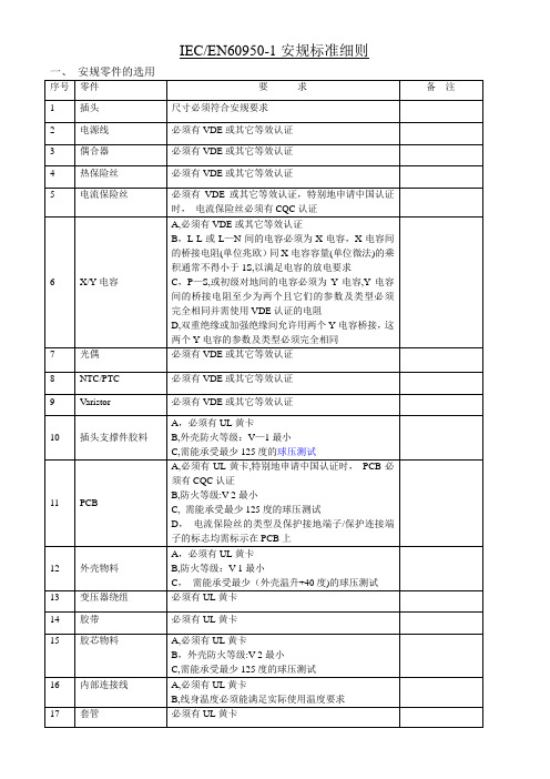
IEC/EN60950-1安规标准细则二、电气间隙及爬电距离1,L-N 间须至少满足基本绝缘2,保险丝两引脚间需至少满足基本绝缘3, 初次级电路之间,光藕初次级之间,变压器初次级之间(含初级绕组/初级PIN/初级铜箔对次级绕组/次级PIN/次级铜箔),Y电容初次级间均需满足双重绝缘或加强绝缘;初级带电部件同外壳外部可触及部位间需满足最少0。
4mm的穿透绝缘或双重绝缘/加强绝缘要求参考IEC60950-1 table 2H,2J,2L,基本绝缘,附加绝缘,加强绝缘(或双重绝缘)需满足以下要求(工作电压以250V AC 或354V峰值计算):基本绝缘/附加绝缘: 电气间隙CL:2。
mm Min, 爬电距离2。
5 mm Min双重绝缘/加强绝缘: 电气间隙CL:4.。
mm Min,爬电距离5.0 mm Min备注1:计算电气间隙及爬电距离,允许对内部零件施加10N的力备注2:计算电气间隙及爬电距离时,污染等级以2级计备注3:计算电气间隙及爬电距离时,物料级别通常为IIIb备注4:计算爬电距离时,允许用插值法三、高压及绝缘要求1备注:开关电源建议用DC电压进行高压测试.2、绝缘电阻IEC/EN60950-1对绝缘电阻无要求.四、正常温升(通常带满载进行测试)1,测试电压a,测试电压为电源电压的+6%- -10%,或b,额定电压为230V时,测试电压为230V的+/—10%,或c, 生产商指定的更宽的电压范围2,测试频率为50HZ 和/或60HZ3, 环境温度最大的环境温度为25度或生产商指定的更大值4, 绕阻允许的最高温度T《零件允许的最高温度+环境温度-生产商指定的最大的环境温度举例:B级绝缘物料允许的最高温度为120度, 测试的环境温度为25度,—若生产商没有指定最大的环境温度,则T《120+25-25,即T《120度(热偶法测试时T还需减10度)-若生产商指定最大的环境温度为40度,则则T《120+25—40,即T《105度(热偶法测试时T还需减10度)具体零件的温度限定见表4B5,正常温升测试的接收标准测试过程中,温度保险丝及电流保险丝不允许动作,零部件温度不得超出表4B的要求,测试后产品需立即通过高压测试五、异常测试(通常带满载进行测试)1, 测试电压a,测试电压为电源电压的+6%- —10%,或b,额定电压为230V时,测试电压为230V的+/-10%,或c, 生产商指定的更宽的电压范围2,测试频率为50HZ 和或60HZ3,环境温度最大的环境温度为25度或生产商指定的更大值4,测试方法a)开路或短路半导体零件和电容b)组合电路中会导致出现能量过分消耗的内部错误c)满足双重绝缘或加强绝缘的Y电容不必进行单一故障测试5,异常测试的接收标准异常测试过程中不允许出现:———火蔓延到设备外部,并且-——发出金属融化物——-外壳出现变形致使电气间隙及爬电距离不符要求-——A级绝缘物料温度超过150度,E级绝缘物料温度超过165度,B级绝缘物料温度超过175度,F 级绝缘物料温度超过190度,H级绝缘物料温度超过210度异常测试过程后不允许出现:—-——-高压失败六、接触电流(泄露电流)———可接触不见及电路没有连接到保护接地时,接触电流0.25mA Max-—-手持设备测试设备端子通过主保护接地端子时,接触电流0。
安规爬电距离与电气间隙

安规爬电距离与电气间隙标准化管理处编码[BBX968T-XBB8968-NNJ668-MM9N]IEC/EN60950 空间距离 /Clearances(min) 爬电距离/Creepage distances(min) 保险丝前 L N 3mm 3mm初级接地零部件 3mm 3mm保险丝本体 3mm 3mm初级次级 5mm 6mmIEC/EN60065 空间距离 /Clearances(min) 爬电距离/Creepage distances(min) (保险丝前)L—N 3mm 3mm初级—接地零部件 3mm 3mm保险丝本体 3mm 3mm初级—次级 6mm 6mmIEC/EN60335 空间距离 /Clearances(min) 爬电距离/Creepage distances(min) (保险丝前)L—N 3mm 3mm初级—接地零部件 3mm 3mm保险丝本体 3mm 3mm初级—次级(Transformer) 6mm 6mm初级—次级(Except Transformer) 6mm 6mmIEC/EN61558 空间距离 /Clearances(min) 爬电距离/Creepage distances(min) (保险丝前)L—N 3mm 3mm初级—接地零部件 3mm 3mm保险丝本体 3mm 3mm初级—次级 6mm安全规格(系列标准)注:1、IEC/EN60065 适用于:家用电子类产品,例如:电视机,录音机,收音机,VCD,DVD,电子琴,复读机......2、IEC/EN61558 适用于:安全变压器及安全隔离变压器,例如:空调内置变压器,按摩椅上的变压器,鱼罐内的变压器等,其实,所有产品均可用此标准,但是,由于此标准要求很严,一般情况下,我们的产品不申请此产品.除非其他标准类没含盖的产品或客人特殊要求.3、IEC/EN60335适应于:家用电器类产品,例如:电池充电器,灯具,微波炉等.电气间隙:两相邻导体或一个导体与相邻带电机壳表面的沿空气测量的最短距离.爬电距离:两相邻导体或一个导体与相邻电机壳表面的沿绝缘表面测量的最短距离.[size=2]安全距离[/size]包括电气间隙(空间距离),爬电距离(沿面距离)和绝缘穿透距离1、电气间隙:两相邻导体或一个导体与相邻电机壳表面的沿空气测量的最短距离.2、爬电距离:两相邻导体或一个导体与相邻电机壳表面的沿绝绝缘表面测量的最短距离.电气间隙的决定:根据测量的工作电压及绝缘等级,即可决定距离一次侧线路之电气间隙尺寸要求,见表3及表4二次侧线路之电气间隙尺寸要求见表5但通常:一次侧交流部分:保险丝前L—N≥, PE(大地)≥,保险丝装置之后可不做要求,但尽可能保持一定距离以避免发生短路损坏电源.一次侧交流对直流部分≥一次侧直流地对大地≥ (一次侧浮接地对大地)一次侧部分对二次侧部分≥,跨接于一二次侧之间之元器件二次侧部分之电隙间隙≥即可二次侧地对大地≥即可附注:决定是否符合要求前,内部零件应先施于10N力,外壳施以30N力,以减少其距离,使确认为最糟情况下,空间距离仍符合规定.爬电距离的决定:根据工作电压及绝缘等级,查表6可决定其爬电距离但通常:(1)、一次侧交流部分:保险丝前L—N≥, 大地≥,保险丝之后可不做要求,但尽量保持一定距离以避免短路损坏电源.(2)、一次侧交流对直流部分≥(3)、一次侧直流地对地≥如一次侧地对大地(4)、一次侧对二次侧≥,如光耦、Y电容等元器零件脚间距≤要开槽.(5)、二次侧部分之间≥即可(6)、二次侧地对大地≥以上(7)、变压器两级间≥以上3、绝缘穿透距离:应根据工作电压和绝缘应用场合符合下列规定:——对工作电压不超过50V(71V交流峰值或直流值),无厚度要求;——附加绝缘最小厚度应为;——当加强绝缘不承受在正常温度下可能会导致该绝缘材料变形或性能降低的任何机械应力时的,则该加强绝缘的最小厚度应为.如果所提供的绝缘是用在设备保护外壳内,而且在操作人员维护时不会受到磕碰或擦伤,并且属于如下任一种情况,则上述要求不适用于不论其厚度如何的薄层绝缘材料;——对附加绝缘,至少使用两层材料,其中的每一层材料能通过对附加绝缘的抗电强度试验;或者:——由三层材料构成的附加绝缘,其中任意两层材料的组合都能通过附加绝缘的抗电强度试验;或者:——对加强绝缘,至少使用两层材料,其中的每一层材料能通过对加强绝缘的抗电强度试验;或者:——由三层绝缘材料构成的加强绝缘,其中任意两层材料的组合都能通过加强绝缘的抗电强度试验.4、有关于布线工艺注意点:如电容等平贴元件,必须平贴,不用点胶如两导体在施以10N力可使距离缩短,小于安规距离要求时,可点胶固定此零件,保证其电气间隙.有的外壳设备内铺PVC胶片时,应注意保证安规距离(注意加工工艺)零件点胶固定注意不可使PCB板上有胶丝等异物.在加工零件时,应不引起绝缘破坏.5、有关于防燃材料要求:热缩套管 V—1或VTM—2以上;PVC套管 V—1或VTM—2以上铁氟龙套管 V—1或VTM—2以上;塑胶材质如硅胶片,绝缘胶带V—1或VTM—2以上PCB板 94V—1以上6、有关于绝缘等级(1)、工作绝缘:设备正常工作所需的绝缘(2)、基本绝缘:对防电击提供基本保护的绝缘(3)、附加绝缘:除基本绝缘以外另施加的独立绝缘,用以保护在基本绝缘一旦失效时仍能防止电击(4)、双重绝缘:由基本绝缘加上附加绝缘构成的绝缘(5)、加强绝缘:一种单一的绝缘结构,在本标准规定的条件下,其所提供的防电击的保护等级相当于双重绝缘各种绝缘的适用情形如下:A、操作绝缘oprational insulationa、介于两不同电压之零件间b、介于ELV电路(或SELV电路)及接地的导电零件间.B、基本绝缘 basic insulationa、介于具危险电压零件及接地的导电零件之间;b、介于具危险电压及依赖接地的SELV电路之间;c、介于一次侧的电源导体及接地屏蔽物或主电源变压器的铁心之间;d、做为双重绝缘的一部分.C、补充绝缘 supplementary insulationa、一般而言,介于可触及的导体零件及在基本绝缘损坏后有可能带有危险电压的零件之间,如:Ⅰ、介于把手、旋钮,提柄或类似物的外表及其未接地的轴心之间.Ⅱ、介于第二类设备的金属外壳与穿过此外壳的电源线外皮之间.Ⅲ、介于ELV电路及未接地的金属外壳之间.b、做为双重绝缘的一部分D、双重绝缘Double insulation Reinforced insulation一般而言,介于一次侧电路及a、可触及的未接地导电零件之间,或b、浮接(floating)的SELV的电路之间或c、TNV电路之间双重绝缘=基本绝缘+补充绝缘注:ELV线路:特低电压电路在正常工作条件下,在导体之间或任一导体之间的交流峰值不超过或直流值不超过60V的二次电路.SELV电路:安全特低电压电路.作了适当的设计和保护的二次电路,使得在正常条件下或单一故障条件下,任意两个可触及的零部件之间,以及任意的可触及零部件和设备的保护接地端子(仅对I类设备)之间的电压,均不会超过安全值.TNV:通讯网络电压电路在正常工作条件下,携带通信信号的电路.。
爬电距离和电气间隙

The Evaluation of Spacings in Electronic Product DesignM. A. LamotheCreepage distance and clearance requirements are tied to a variety of electrical and environmental factors addressed by safety standards.Equipment intended to be approved to IEC standards must be designed with spacings between conductive parts that are sufficient to ensure user safety in the presence of hazardous voltages. Designers need to be familiar with the effects of pollution degree, overvoltage category, and working voltage on their decisions regarding spacing distances. The role of creepage distance and clearance in the designing of an electrical product with hazardous voltages present is often imperfectly understood, as is the fact that these influences represent a three-dimensional problem. Clearance is the shortest distance between two conductive parts, or between a conductive part and the bounding surface of the equipment, measured through air. Components that are mounted above the printed circuit board (PCB) must also be considered in the evaluation of clearance. Creepage distance is the shortest path between two conductive parts, or between a conductive part and the bounding surface of the equipment, measured along the surface of the insulation. All conductive parts are considered in evaluating creepage distance, including the pads around soldered connections. The typical solder resist does not reduce the creepage distance requiredon a PCB.These requirements for spacings—creepage distance and clearance—can best be understood by looking at the electrical and environmental factors that affect them. Such factors are the pollution degree of the environment that the equipment will be installed in, the overvoltage category of the equipment's power source, the working voltage, the comparative tracking index of the substrate material, and the specified maximum installation altitude. This article examines the relationship of these elements to spacing requirements and illustrates the practical application of the concepts. Figure 1 depicts the general influence of each factor on necessary clearance and creepage distance. All dimensions cited come from the third edition of "Safety of Information Technology Equipment," CSA CAN/CSA-C22.2 No. 60950-00/UL 60950.1Figure 1. The general effect of electrical and environmental factors on creepagedistance and clearance: (a) pollution degree, (b) overvoltage category, (c) workingvoltage, (d) the previous factors cumulatively, (e) comparative tracking index(applies to creepage distance only), and (f) altitude (applies to clearance distanceonly).Pollution DegreeFour levels of pollution degree signify increasing ambient influence on the internal equipment environment and have different effects on product design. Definitions are based on IEC 60664.2 Pollution Degree 1 refers to a condition of no pollution or only dry, nonconductive pollution. Likely to be characteristic of clean room equipment, this type of pollution has no influence. Only components or subassemblies that are adequately enclosed by enveloping or hermetic sealing to prevent ingress of dirt and moisture qualify to use Pollution Degree 1 spacings.Pollution Degree 2 is nonconductive pollution of the sort where occasionally a temporary conductivity caused by condensation must be expected. This is the usual pollution degree used for equipment being evaluated to 60950 and is suitable for equipment employed in an office environment.Pollution Degree 3 covers conductive pollution and dry, nonconductive pollution that becomes conductive owing to condensation that can be expected. The local internal environment of the equipment is subject to conductive pollution because the device is permanently or temporarily exposed to the outdoors.Pollution Degree 4 refers to pollution that generates persistent conductivity caused, for instance, by conductive dust or by rain or snow. This category is not applicable to products covered in 60950.Again, the higher the pollution degree, the worse the environment. Greater spacings are required in response to higher degrees of pollution in order to prevent breakdown between parts of the circuit or equipment (see Figure 1a).Overvoltage CategoryThe overvoltage category of the power source used to run the equipment also has an effect on product design. The definitions presented here are based on IEC 60664.Overvoltage Category I refers to the signal level and encompasses secondary circuits, special equipment or parts of equipment, telecommunications devices, and the like, which experience smaller transient overvoltages than normal in Overvoltage Category II. Category I spacings are usually employed for battery-powered or safety extra-low-voltage (SELV)—powered equipment where there are not likely to be power-source transients.Overvoltage Category II is local level, covering appliances, portable equipment, etc., with smaller transient overvoltages than those characteristic of Overvoltage Category III. This category applies from the wall plug to the power-supply isolation barrier (transformer). The typical office and small plant environment is Overvoltage Category II, so most equipment evaluated to the requirements of 60950 are considered to belong in that classification.Overvoltage Category III refers to the distribution level, that is, building wiring and fixed installations. This level experiences smaller transient overvoltages than occur in Overvoltage Category IV. A large industrial plant would be considered Overvoltage Category III. Equipment for use in this environment must receive special consideration for both pollution degree and overvoltage category. Many standards require that the environment be specified in the product manual.Overvoltage Category IV refers to the primary supply level: overhead lines, cable systems, and so on. This category is not relevant to most product standards.Just as higher pollution degree levels require greater spacing in product designs, so do higher overvoltage category levels (see Figure 1b).Working VoltageWorking voltage is defined in IEC 60664 as “the highest rms [root-mean-square] value of the ac or dc voltage that may occur locally across any insulation at rated supply voltage, transients being disregarded,” in open-circuit conditions or in normal use. All voltages must be measured using a true rms meter or scope. A scope has to be used to determine repetitive peak voltages because the spikes may be very narrow (and thus have a low rms value) but also high in voltage, which could contribute to the occurrence of breakdown.All of the following requirements apply in determining the working voltages.•The value of the rated voltage or the upper voltage of the rated voltage range is used for working voltage between a primary circuit and ground, and it is taken into account in determining the working voltage between a primary circuit and a secondary circuit.•Ungrounded accessible conductive parts are assumed to be grounded.• A transformer winding or other part that is floating (i.e., that is not connected to a circuit that establishes its potential relative to earth) is assumed to be grounded at the point by which the highest working voltage is obtained.•Where double insulation is used, the working voltage across the basic insulation is determined by imagining a short circuit across the supplementary insulation, and vice versa. For double insulation between transformer windings, the short circuit is assumed to take place at the point where the highest working voltage is produced in the other insulation. (See the section "Types of Insulation,"below, for definitions.)•For insulation between two transformer windings, the highest voltage between any two points in the two windings is used, taking into account external voltages to which the windings will be connected.•For insulation between a transformer winding and another part, the highest voltage between any point on the winding and the other part is used. For a working voltage to be used in determining clearances for primary circuits:•The peak value of any superimposed ripple is included for dc voltages.•Nonrepetitive transients, such as those due to atmospheric disturbances, are disregarded. (It is assumed that any such transient in a secondary circuit will not exceed the transient rating of the primary circuit.)•The voltage of any extra-low-voltage (ELV), SELV, or telecommunication-network-voltage (TNV) circuit is regarded as zero.•The maximum repetitive peak value is used for repetitive peak voltages exceeding the peak values of the mains supply voltage. For a working voltage to be used in determining clearances for secondary circuits:•The peak value of any superimposed ripple is included for dc voltages.•The peak value is used for nonsinusoidal waveforms. For a working voltage to be used in determining creepage distance:•The actual rms or dc value is used.•If the dc value is used, any superimposed ripple is ignored.Note that rms voltages are used in calculating creepage distance and that peak or dc voltages are employed to calculate clearances. The higher the working voltage, the greater the spacings required (see Figure 1c). Figure 1d shows the cumulative effect on product design of pollution degree, overvoltage category, and working voltage.Comparative Tracking IndexThe comparative tracking index (CTI) of the material affects the creepage distance. The CTI value is a measure of the resistance to surface tracking that a particular material exhibits under specific test conditions. The lower the CTI for that material, the greater the creepage distancerequired (see Figure 1e). Materials fall into four material groups: I (CTI > 600), II (CTI > 400 and < 600), IIIa (CTI > 175 and < 400), and IIIb (CTI > 100 and < 175). Most pcbs have a value of 175. Installation AltitudeAltitude with reference to sea level affects the required clearance. Most standards use 2000 m as the baseline. Higher installation elevations require the addition of a correction factor because the lower atmospheric pressure at high altitude has less resistance to breakdown. For elevations above 2000 m, the required clearance is increased by the following factors: to 3000 m, 1.14; from 3000 to 4000 m, 1.29; and from 4000 to 5000 m, 1.48 (see Figure 1f).Types of InsulationWherever the operator, under all normal conditions and under any single-fault condition, can contact a part, there must be no hazard. As a consequence, the product designer must define the type of insulation required as a minimum between various areas of the device. For example, primary-to-SELV will require double or reinforced insulation.Also, if an accessible conductive component that is not grounded could become energized by the failure of basic insulation of another component, then supplementary insulation must be applied to protect the accessible ungrounded component. An example might be a metal handle on a power switch.Basic insulation provides basic protection against electric shock. This insulation is used between parts at hazardous voltages and a grounded conductive part or SELV part, between primary and the grounded screen or core of a primary power transformer, and as an element of double insulation.Supplementary insulation is independent insulation applied in addition to the basic insulation in order to reduce the risk of electric shock in the event of failure of the latter. Supplementary insulation is generally used between an accessible conductive part and a part that could become energized if the basic insulation failed or else as an element of double insulation. This insulation is required to ensure protection of the operator should basic insulation fail.Double insulation is composed of basic and supplementary insulation. It is used between an ungrounded conductive part or floating SELV circuit and a primary circuit.Reinforced insulation is a single-insulation system that provides the same protection against electric shock as double insulation. Unlike basic or supplementary insulation materials, reinforced insulation may consist of layers of material that cannot themselves be tested singly.Functional insulation is insulation needed for correct equipment operation. It does not protect against electric shock. Functional insulation would be used between parts having different potentials or between ELV or SELV circuits and grounded conductive parts. This type of insulation replaces operational insulation in the third edition of IEC 60950.In summary, basic and supplementary types of insulation each consist of a single layer, double insulation involves two layers, and reinforced insulation is a single layer that is equivalent to two layers of insulation. Table I charts the different types of insulation required between pairs of device components.Device Areas B R S F Primary winding to primary winding xPrimary winding to grounded screen xPrimary winding to insulated body xPrimary winding to double-insulatedxbodyPrimary winding to hazardous secondary xPrimary winding to ELV or groundedxSELVPrimary winding to ungrounded SELV xGrounded screen to insulated body xGrounded screen to double-insulatedx bodyGrounded screen to hazardousxsecondaryGrounded screen to ELV or SELV xDouble insulation to double-insulatedx bodyDouble insulation to hazardousxsecondaryDouble insulation to ELV xDouble insulation to SELV x Hazardous secondary to ELV xHazardous secondary to groundedxSELVHazardous secondary to ungroundedxSELVELV to grounded SELV x Grounded SELV to ungrounded SELV x TNV to primary xTNV to grounded or ungrounded SELV xTNV to ELV xTNV to grounded hazardous secondary xTNV to ungrounded hazardousx x secondaryTable I. Types of insulation required between device areas: B = basic, R = reinforced, S = supplementary, and F = functional.The Concepts in ApplicationTo determine the required creepage distance and clearance spacings for an electronic product, the best method is to first draw a block diagram of the design (see Figure 2) from which a table of the required spacings can be prepared (see Table II). For example, the primary section of a power supply is treated as a block. Spacings are examined between hot and neutral to groundand between all primary and secondary parts. Each circuit should be regarded as a block.Figure 2. A block diagram of the electronic device for which the spacing requirements in Table II have been calculated.Required CreepageDistance Location in System Insulation Type Maximum WorkingVoltage (V ac) mm CTI ValueRequired Clearance (mm) Test Voltage(V ac) A B 230 2.5 175 2.0 1500 B D 260 6.4 175 4.0 3000 C B 460* 6.3 175 3.2 1674 D B 460* 6.3 175 3.2 1674 E D 260 6.4 175 4.0 3000 F D 260 6.4 175 4.0 3000 G B 230 2.5 175 2.0 1500 H B 230 2.5 175 2.0 1500 I B 460* 6.3 175 3.2 1674 JF2302.51751.51500*Working voltage based on the rating of the relay contact plus 230 V.Table II. Tabulation of creepage and clearance distances required for the system diagrammed inFigure 2, which is characterized by Pollution Degree 2 and Overvoltage Category II.Insulation types are basic (B), double (D), and functional (F). Source: Tables 2L and 2H of IEC60950.It is important to note that the voltages of each block are not added together if they are powered from the same source (i.e., across a transformer). In the case of a relay contact where the contacts are connected to a different source, the two voltages are added together to determine the working voltage.ConclusionThe evaluation of electronic device spacings is essential in the designing of products that are to be approved to any of the IEC product safety standards. The standard should always be consulted. The information provided in this article is intended to be illustrative and to provide a basic understanding of the principles involved, and should not be used in actual product design in lieu of authoritative reference documents.Calculating Creepage and Clearance Early Avoids Design Problems LaterOne of the most common errors uncovered by product safety engineers stems from manufacturers and designers failing to fully investigate a product's creepage and clearance distances.It is not unusual for manufacturers to find that a product fails the creepage and clearance distance test because of miscalculations or simply because the distance between twocomponents was overlooked. Design engineers, especially printed circuit board (PCB)designers, are often not aware of the reasons for using creepage and clearance distances.Selecting the appropriate tables in the standard and applying them properly to a design are key to avoiding problems later.Last-minute failure can also arise because design engineers do not seek input from the product safety engineers in the early design stages. Designers sometimes assume that all safety issues relating to creepage and clearance have been addressed, only to discover spacing problemsonce the product is built.Basic DefinitionsCreepage Distance. Creepage is the shortest path between two conductive parts (or between a conductive part and the bounding surface of the equipment) measured along the surface of the insulation. A proper and adequate creepage distance protects against tracking, a process that produces a partially conducting path of localized deterioration on the surface of an insulating material as a result of the electric discharges on or close to an insulation surface. The degree of tracking required depends on two major factors: the comparative tracking index (CTI) of the material and the degree of pollution in the environment. Used for electrical insulating materials,the CTI provides a numerical value of the voltage that will cause failure by tracking during standard testing. IEC 112 provides a fuller explanation of tracking and CTI.1 Tracking that damages the insulating material normally occurs because of one or more of the following reasons: •Humidity in the atmosphere.•Presence of contamination.•Corrosive chemicals.•Altitude at which equipment is to be operated.Clearance Distance. Clearance is the shortest distance between two conductive parts (or between a conductive part and the bounding surface of the equipment) measured through air. Clearance distance helps prevent dielectric breakdown between electrodes caused by the ionization of air. The dielectric breakdown level is further influenced by relative humidity, temperature, and degree of pollution in the environment.When designing a switch-mode power supply for use in information technology (IT) equipment, a typical rule of thumb is to allow an 8-mm creepage distance between primary and secondary circuits, and a 4-mm distance between primary and ground. If these dimensions are allowed for during the design stage, there is a high probability (95%) that no failure will occur with respect to creepage or clearance when the final product is submitted for test.Working Voltages. A working voltage is the highest voltage to which the insulation under consideration is (or can be) subjected when the equipment is operating at its rated voltage under normal use conditions. The appropriate creepage and clearance values can be determined from the figures provided in the relevant tables in EN 60950.2 These values must sometimes be calculated. To use Tables I–IV (2H, 2J, 2K, and 2L of the standard), the following factors must be considered: determination of working voltages, pollution degree of the environment, and the overvoltage category of the equipment's power source.When measuring working voltages, it is important to measure both peak and root-mean-square (rms) voltages. The peak value is used to determine the clearance, and the rms value is used to calculate creepage. For example, if one measures a peak voltage of 670 V between two pins of a switching transformer in a switch-mode power supply, the clearance distance between primary and secondary circuits must be calculated using Table I. If the unit is powered via 240 V mains and has a pollution degree of 2, the figures in the center row (marked 300 V rms sinusoidal) and center column (since the mains voltage is >150 V and < 300 V) are used to establish the required clearance distance. In this case, the value for reinforced insulation is 4 mm. One then turns to Table II (Table 2J of EN 60950), which provides additional clearance based on the working voltages and pollution degree. (The middle column was used for calculating this example.) The appropriate row in that column covers the actual repetitive peak insulation working voltage. In this example, the value would be 0.8 mm for reinforced insulation. Adding the two figures together gives a total of 4.8 mm clearance distance. Similarly, if a voltage of 337 V rms was measured between the two pins of the switching transformer, Table IV (2L of the standard) must be used to calculate the creepage distance between the primary and secondary circuits. Assuming pollution degree 2 and material group IIIb, the required creepage distance for basic insulation would be 3.5 mm using linear interpolation. For reinforced insulation, the values for creepage distances are double the values provided in the table for basic insulation. In this case, the required creepage for reinforced insulation would be 7 mm.Funtional, Basic, and Supplementary Insulation Pollution Degree 1 Pollution Degree 2 Pollution Degree 3Working Voltage V Rms or DcMaterial GroupMaterial GroupMaterial GroupI, II, IIIa, or IIIbI II IIIa, or IIIb I II IIIa, or IIIb <50 0.6 0.9 1.2 1.5 1.7 1.9 100 0.7 1.0 1.4 1.8 2.0 2.2 125 0.8 1.1 1.5 1.9 2.1 2.4 150 0.8 1.1 1.6 2.0 2.2 2.5 200 1.0 1.4 2.0 2.5 2.8 3.2 250 1.3 1.8 2.5 3.2 3.8 4.0 300 1.6 2.2 3.2 4.0 4.5 5.0 400 2.0 2.6 4.0 5.0 5.66.3600 3.2 4.5 5.3 8.09.5 10.0800 4.0 5.6 8.0 10.0 11.0 12.51000Use the clearance from the appropriate tables5.07.110.012.5 14.0 16.0Linear interpolation is permitted between the nearest two points, the calculated spacing being rounded to the next higher 0.1-mm increment.Table IV. Table 2L of the standard provides minimum creepage distances (creepage distances in millimeters).The use of these tables is explained in sections 2.10.3–2.10.4 of EN 60950. Measurements should be accurate and repeatable and should also consider the end application. Pollution Degrees and OvervoltagesPollution degree is divided into four categories. The following definitions are based on those in IEC 60664.3•Pollution degree 1. No pollution or only dry, nonconductive pollution occurs. The pollution has no influence (example: sealed or potted products).• Pollution degree 2. Normally only nonconductive pollution occurs. Occasionally a temporaryconductivity caused by condensation must be expected (example: product used in typical office environment).• Pollution degree 3. Conductive pollution occurs, or dry, nonconductive pollution occurs thatbecomes conductive due to expected condensation (example: products used in heavy industrial environments that are typically exposed to pollution such as dust).• Pollution degree 4. Pollution generates persistent conductivity caused, for instance, by conductivedust or by rain or snow.The overvoltage, also known as installation, category is also divided into four categories according to IEC 60664.•Overvoltage category I. Signal level (special equipment or parts of equipment), with smaller transient overvoltages than overvoltage category II.•Overvoltage category II. Local level (appliances and portable equipment), with smaller transient overvoltages than overvoltage category III.•Overvoltage category III. Distribution level (fixed installations) with smaller transient overvoltages than overvoltage category IV.•Overvoltage category IV. Primary supply level (overhead lines, cable systems, etc.). This category is not relevant to most product standards.Typically, most standards are based on conditions being pollution degree 2 and overvoltage category II. It is important to note that as working voltage, pollution degree, overvoltage category, and altitude increase, the creepage and clearance distances also increase. The altitude is particularly important when testing to EN 61010.4Creepage and Clearance in PracticeEach part of a circuit must be studied to determine the necessary insulation grade. Table 2G in EN 60950 describes common applications of insulation. For example, establishing the required creepage and clearance between a primary circuit and an ungrounded safety extra low voltage (SELV) circuit requires reinforced insulation. By measuring and establishing both the working voltage and the pollution degree, the appropriate row and column in Table 2H (and if necessary Table 2J) determine the minimum clearance distance needed. For one test, the internal components and parts in both primary and secondary circuits are subjected to a steady force of 10 N, and certain minimum clearance distances must be maintained during the test.Because the primary circuit is an internal circuit connected directly to the external supply mains, this circuit typically contains hazardous voltage. A secondary circuit, which has no direct connection to primary power, may or may not be hazardous. Nonhazardous circuits are classified as SELV.Dc input products, however, can be treated in one of two ways. They can be considered as being fed by an extra-low-voltage circuit, or as hazardous secondary voltages. This would mean that the clearances could be calculated using Table III rather than Table I, requiring slightly smaller clearance distances. Dc input products can also be considered as being fed by SELV secondary circuits, depending upon the end application. If isolation is needed, then Table III of the standard is used. However, if isolation is not required in the end application, then clearances are waived, and only operational insulation is required.Simple Design TipsAs IT products continue to get smaller, it is more important than ever to have a good and calculated PCB design that not only reduces electromagnetic interference emissions, but that also reduces creepage and clearance problems. Where shortage of space on a PCB is an issue, especially between primary and SELV circuits, techniques such as slots or grooves can be used to attain desired creepage distance. Slots must be wider than 1 mm; otherwise, they are not considered acceptable. For a groove (>1 mm wide) the only depth requirement is that the existing creepage plus the width of the groove and twice the depth of the groove must equal or exceed the required creepage distance. The slot or groove should not weaken the substrate to a point that it fails to meet mechanical test requirements.Another solution is to design the PCB so that components are mounted flat on the board rather than positioned vertically. This layout overcomes problems that might arise from the 10- N push test required in EN 60950. A minimum of 8 mm separation between primary and secondary circuits also prevents problems. When semiconductors operating at hazardous voltages are mounted on grounded or floating heat sinks, certain precautions must be taken to ensure compliance with EN 60950. If heat sinks happen to be live (and they can be), they should be marked accordingly to warn service personnel. Generally, a semiconductor's plastic enclosure is considered as operational (necessary for correct operation of the equipment) or, in some cases, as only basic insulation. Therefore, depending on the heat sink's grounding arrangement, the semiconductor requires either basic or reinforced insulation.It is equally important to consider creepage and clearance even when using UL-recognized power-switching semiconductors. Although these products carry a recognition mark, the manufacturer's data sheets must be examined to ensure that the components are suitable for the intendedapplication.The working voltages of the circuit must be taken into account. Transistors with built-in reinforced insulation (body thicker than 0.4 mm) must also still meet the spacing requirements at their legs. Some designers mistakenly assume that UL certification eliminates the need for further examination.TroubleshootingIn some cases—in particular for switch-mode power supplies—the design topology can lead to the need for higher creepage distance in the switching transformer. In such situations, the use of a wider margin tape (also known as saddle tape) may not be practical; therefore, the use of multilayer insulated wire (also known as triple-insulated wire) is highly recommended. When using triple-insulated wire, it is important to remember that such wire must satisfy the requirements described in Annex U of EN 60950. Lack of adequate creepage and clearance distance between a component in a primary circuit to a component in the SELV circuit is a common cause of product failure. A typical short-term solution is to place an insulating material, such as Mylar sheet, with appropriate thickness and dielectric withstand voltage, between the two parts, ensuring that the sheet is mechanically secure. Room-temperature vulcanizing sealant, a silicone paste cured at room temperature, or a similar material, is used not only as a means of bonding components together for mechanical purposes, but also to overcome clearance problems. However, materials that are used to compensate for clearance problems must be UL recognized, particularly if a product is to be sold in North America.ConclusionCalculation and measurement of creepage and clearance distances are among the most important parts of all safety standards, and therefore it is important for design engineers to consult the product safety engineers throughout the design stages to avoid any failure at the test house before a product is launched into the market.Creepage and clearance distances not only apply to the PCB, but also to the components (especially magnetic components) that are mounted on the PCB. It is also important to note that as working voltage, pollution degree, overvoltage category, and altitude increase, both the creepage and clearance distances also increase.。
安规之电气间距和爬电距离

广州致远电子有限公司
示波器探头
交L
流
电N
网
输 入
PE
变压器
一次 电路
光耦
二次 电路
+Vo
RL -Vo
电源产品
图1 假如开关电源输入只有 L、N 则测试图如下图 2 所示:
示波器探头
交 流L变压器来自电一次网
电路
输N
入
光耦
二次 电路
+Vo
RL -Vo
图2 实例分析
实测 100~240VAC 输入开关电源初次级最大电压波形如下图 3 所示,工作电压峰值为 500V,工作电压有效值为 265V,根据表 2J 可知交流电网电源瞬态电压为 2500V。
爬电距离计算:按照污染等级 2、材料类别Ⅲ可知 265V 有效值电压在表 2N 的 250V 和 320V 之间,而 250V 时基本绝缘为 2.5mm,320V 的基本绝缘为 3.2mm,即 265V 电压基本
绝缘为
即加强绝缘为 5.3mm 海拔对安全距离影响
以上查询的安全间距只适用于海拔 2000m 以下,而对于海拔 2000 以上的情况,安全 距离需要乘以一定系数。标准 GB/T 16935.1 的表 A2 给出了海拔与系数的对应关系,比如 海拔 5000mm 时,最小安全间距需要乘以 1.48 倍。
1、 根据交流电网电压有效值和过电压类别确认交流电网电源瞬态电压(由附录 Z 和表 2J 确定); 表 2J 交流电网电源瞬态电压
2、 首先确定污染等级,再根据实测两点峰值工作电压 B 和上述确认的交流电网电源瞬 态电压值可确定最小电气间隙为 C1(由表 2K 确定);
表 2K 一次电路绝缘以及一次电路与二次电路之间绝缘最小电气间隙(海拔 2000m 以 下) 单位为 mm
安规爬电距离与电气间隙
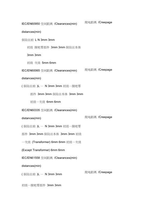
IEC/EN60950 空间距离/Clearances(min) distances(min)保险丝前L N 3mm 3mm初级接地零部件3mm 3mm 保险丝本体3mm 3mm初级次级5mm 6mmIEC/EN60065 空间距离/Clearances(min) distances(min)( 保险丝前)L —N 3mm 3mm 初级—接地零部件3mm 3mm 保险丝本体3mm 3mm初级—次级6mm 6mmIEC/EN60335 空间距离/Clearances(min) distances(min)( 保险丝前)L —N 3mm 3mm 初级—接地零部件3mm 3mm 保险丝本体3mm 3mm 初级—次级(Transformer) 6mm 6mm 初级—次级(Except Transformer) 6mm 6mmIEC/EN61558 空间距离/Clearances(min) distances(min)( 保险丝前)L —N 3mm 3mm初级—接地零部件3mm 3mm 爬电距离/Creepage 爬电距离/Creepage 爬电距离/Creepage 爬电距离/Creepage保险丝本体3mm 3mm初级—次级5.5mm 6mm安全规格(系列标准)注:1、IEC/EN60065适用于:家用电子类产品,例如:电视机,录音机,收音机,VCD,DVD,电子琴,复读机……2 、IEC/EN61558 适用于: 安全变压器及安全隔离变压器, 例如:空调内置变压器, 按摩椅上的变压器,鱼罐内的变压器等, 其实,所有产品均可用此标准, 但是, 由于此标准要求很严, 一般情况下, 我们的产品不申请此产品. 除非其他标准类没含盖的产品或客人特殊要求3 、IEC/EN60335适应于:家用电器类产品,例如:电池充电器,灯具,微波炉等.电气间隙: 两相邻导体或一个导体与相邻带电机壳表面的沿空气测量的最短距离.爬电距离: 两相邻导体或一个导体与相邻电机壳表面的沿绝缘表面测量的最短距离.[size=2] 安全距离[/size]包括电气间隙(空间距离), 爬电距离(沿面距离)和绝缘穿透距离1 、电气间隙: 两相邻导体或一个导体与相邻电机壳表面的沿空气测量的最短距离.2、爬电距离: 两相邻导体或一个导体与相邻电机壳表面的沿绝绝缘表面测量的最短距离.电气间隙的决定: 根据测量的工作电压及绝缘等级, 即可决定距离一次侧线路之电气间隙尺寸要求, 见表 3 及表 4 二次侧线路之电气间隙尺寸要求见表5但通常:一次侧交流部分:保险丝前L—N>2.5mm,L.N PE(大地)>2.5mm, 保险丝装置之后可不做要求, 但尽可能保持一定距离以避免发生短路损坏电源.一次侧交流对直流部分》2.0 mm一次侧直流地对大地》2.5mm (一次侧浮接地对大地)一次侧部分对二次侧部分》4.0mm跨接于一二次侧之间之元器件二次侧部分之电隙间隙》0.5mm即可二次侧地对大地》1.0mm即可附注:决定是否符合要求前,内部零件应先施于10N力,外壳施以30N力,以减少其距离, 使确认为最糟情况下, 空间距离仍符合规定.爬电距离的决定:根据工作电压及绝缘等级, 查表 6 可决定其爬电距离但通常:(1)、一次侧交流部分:保险丝前L—N>2.5mm,L.N大地》2.5mm, 保险丝之后可不做要求, 但尽量保持一定距离以避免短路损坏电源.(2) 、一次侧交流对直流部分》2.0mm(3) 、一次侧直流地对地》4.0mm如一次侧地对大地⑷、一次侧对二次侧》6.4mm,如光耦、Y电容等元器零件脚间距冬6.4mm 要幵槽.⑸、二次侧部分之间》0.5mm即可⑹、二次侧地对大地》2.0mm以上⑺、变压器两级间》8.0mm以上3、绝缘穿透距离: 应根据工作电压和绝缘应用场合符合下列规定:――对工作电压不超过50V(71V交流峰值或直流值),无厚度要求;——附加绝缘最小厚度应为0.4mm;――当加强绝缘不承受在正常温度下可能会导致该绝缘材料变形或性能降低的任何机械应力时的, 则该加强绝缘的最小厚度应为0.4mm. 如果所提供的绝缘是用在设备保护外壳内, 而且在操作人员维护时不会受到磕碰或擦伤, 并且属于如下任一种情况, 则上述要求不适用于不论其厚度如何的薄层绝缘材料;――对附加绝缘, 至少使用两层材料, 其中的每一层材料能通过对附加绝缘的抗电强度试验; 或者:――由三层材料构成的附加绝缘, 其中任意两层材料的组合都能通过附加绝缘的抗电强度试验; 或者:――对加强绝缘, 至少使用两层材料, 其中的每一层材料能通过对加强绝缘的抗电强度试验; 或者:由三层绝缘材料构成的加强绝缘, 其中任意两层材料的组合都能通过加强绝缘的抗电强度试验.4、有关于布线工艺注意点: 如电容等平贴元件,必须平贴,不用点胶如两导体在施以10N力可使距离缩短,小于安规距离要求时,可点胶固定此零件, 保证其电气间隙.有的外壳设备内铺PVC胶片时,应注意保证安规距离(注意加工工艺)零件点胶固定注意不可使PCB板上有胶丝等异物. 在加工零件时, 应不引起绝缘破坏.5、有关于防燃材料要求:热缩套管V —1或VTM—2以上;PVC套管V —1或VTM—2以上铁氟龙套管V —1或VTM—2以上;塑胶材质如硅胶片,绝缘胶带V—1或VTM—2 以上PCB板94V —1 以上6、有关于绝缘等级(1) 、工作绝缘:设备正常工作所需的绝缘(2) 、基本绝缘: 对防电击提供基本保护的绝缘(3) 、附加绝缘: 除基本绝缘以外另施加的独立绝缘, 用以保护在基本绝缘一旦失效时仍能防止电击(4) 、双重绝缘: 由基本绝缘加上附加绝缘构成的绝缘(5) 、加强绝缘: 一种单一的绝缘结构, 在本标准规定的条件下, 其所提供的防电击的保护等级相当于双重绝缘各种绝缘的适用情形如下A、操作绝缘oprational insulationa、介于两不同电压之零件间b、介于ELV电路(或SELV电路)及接地的导电零件间.B、基本绝缘basic insulationa、介于具危险电压零件及接地的导电零件之间;b、介于具危险电压及依赖接地的SELV电路之间;c、介于一次侧的电源导体及接地屏蔽物或主电源变压器的铁心之间d、做为双重绝缘的一部分.C、补充绝缘supplementary insulationa、一般而言,介于可触及的导体零件及在基本绝缘损坏后有可能带有危险电压的零件之间, 如:I、介于把手、旋钮,提柄或类似物的外表及其未接地的轴心之间.U、介于第二类设备的金属外壳与穿过此外壳的电源线外皮之间.川、介于ELV电路及未接地的金属外壳之间.b、做为双重绝缘的一部分D、双重绝缘Double insulation Reinforced insulation一般而言, 介于一次侧电路及a、可触及的未接地导电零件之间,或b、浮接(floating) 的SELV的电路之间或c、TNV电路之间双重绝缘=基本绝缘+补充绝缘注:ELV线路:特低电压电路在正常工作条件下, 在导体之间或任一导体之间的交流峰值不超过42.4V或直流值不超过60V的二次电路.SELV电路:安全特低电压电路.作了适当的设计和保护的二次电路, 使得在正常条件下或单一故障条件下任意两个可触及的零部件之间, 以及任意的可触及零部件和设备的保护接地端子(仅对I 类设备)之间的电压,均不会超过安全值.TNV:通讯网络电压电路在正常工作条件下, 携带通信信号的电路.。
1、爬电距离与电气间隙_图文解释详解
电气间隙和爬电距离的测量方法电气间隙Clearance在两个导电零部件之间或导电零部件与设备防护界面之间测得的最短空间距离。
即在保证电气性能稳定和安全的情况下,通过空气能实现绝缘的最短距离。
电气间隙的大小和老化现象无关。
电气间隙能承受很高的过电压,但当过电压值超过某一临界值后,此电压很快就引起电击穿,因此在确认电气间隙大小的时候必须以设备可能会出现的最大的内部和外部过电压(脉冲耐受电压为依据)。
在不同场合使用同一电气设备或运用过电压保护器时所出现的过电压大小各不相同。
因此根据不同的使用场合将过电压分为Ⅰ至Ⅳ四个等级。
爬电距离:沿绝缘表面测得的两个导电零部件之间或导电零部件与设备防护界面之间的最短路径。
即在不同的使用情况下,由于导体周围的绝缘材料被电极化,导致绝缘材料呈现带电现象。
此带电区(导体为圆形时,带电区为环形)的半径,即为爬电距离;爬电距离在绝缘材料表面会形成泄漏电流路径。
若这些泄漏电流路径构成一条导电通路,则出现表面闪络或击穿现象。
绝缘材料的这种变化需要一定的时间,它是由长时间加在器件上的工作电压所引起的,器件周围环境的污染能加速这一变化。
因此在确定端子爬电距离时要考虑工作电压的大小、污染等级及所运用的绝缘材料的抗爬电特性。
根据基准电压、污染等级及绝缘材料组别来选择爬电距离。
基准电压值是从供电电网的额定电压值推导出来的。
随着科学技术的迅猛发展,人们的生活水平的不断提高,越来越多的电子产品进入我们的家庭,为保证使用者的人身安全,世界各国均有相关法规以约束电器产品对人身造成的各种伤害。
因此,安全性设计在产品的整个设计过程中有着至关重要的作用,其中安全距离是在产品设计中最重要的部分之一。
在电气间隙、爬电距离实际测量中往往有不同的结果差异、本篇结合自身实际工作,就电气间隙,爬电距离的安全标准要求做一下概括总结,谈谈以下几点理解。
一.名词解释:1、安全距离包括电气间隙(空间距离),爬电距离(沿面距离)和绝缘穿透距离。
- 1、下载文档前请自行甄别文档内容的完整性,平台不提供额外的编辑、内容补充、找答案等附加服务。
- 2、"仅部分预览"的文档,不可在线预览部分如存在完整性等问题,可反馈申请退款(可完整预览的文档不适用该条件!)。
- 3、如文档侵犯您的权益,请联系客服反馈,我们会尽快为您处理(人工客服工作时间:9:00-18:30)。
想了解 IEC/ UL 60950-1:2000 安全标准如何影响电源供电或电池供电的信息类产品的设计吗?需要变更设计,但却没把握 IEC/ UL 60950-1:2000 的规定对于变更的设计有何影响?本文的问答内容旨在协助您符合 IEC/ UL 60950-1:2000 的安全要求。
第一部分沿面距离 (Creepage Distance)
IEC/ UL 60950-1:2000 最小沿面距离的规定载录于 2.10.4 条款中。
敬请参考表 2L 以了解各产品应有的沿面距离要求。
若您的产品所测出的工作电压介于表中指定的两个工作电压值之间,您可利用线性内插法 (Linear Interpolation) 计算出所需要的沿面距离。
请参见表 2L 之附注2。
现在就由以下的举例,示范线性插入法的计算运用。
范例 = 电路信息
输入电压:100-240V AC
测出的工作电压:365 Vms, 890 V peak
污染等级:2
材料类别:IIIa 或 IIIb
Q1a:如何计算基本绝缘需要的沿面距离?
300V 需要的沿面距离 = 3.2mm
400V 需要的沿面距离 = 4.0mm
(4.0-3.2)÷(400-300)×65=0.52
3.2+0.52=3.72
A1a. 基本绝缘需要的的最小沿面距离 = 3.8mm
注意事项:
须根据表 2L 之附注2,以无条件进入的方式算到最接近的 0.1 mm 单位。
Q1b. 如何计算加强绝缘 (Reinforced Insulation) 需要的沿面距离?
公式:(基本绝缘需要的沿面距离) ×2
==== > 3.72×2=7.44
A1b. 加强绝缘需要的的最小沿面距离 = 7.5 mm
注意事项:
须根据表 2L 之附注2,以无条件进入的方式算到最接近的 0.1 mm 单位。
须先将基本绝缘所需的最小沿面距离加倍后,再用无条件进入的方式算到最接近的 0.1 mm 单位。
如果基本绝绿的沿面距离已先采用无条件进入,然后再加倍计算,则计算结果会有 0.1mm 单位的误差。
根据 2.10.4 条款的第三项,万一最小沿面距离小于最小隔空间隙 (Clearance),则以最小隔空直线间隙做为沿面距离的间距。
第二部分隔空间隙 (Clearance)
以下将说明如何针对上例的加强绝缘要求,算出最小的隔空间隙。
敬请参照 2.10.3.2 条款的表 2H 及表 2J 以进一步了解您的设备之隔空间隙要求。
Q2. 如何计算加强绝缘所需要的隔空间隙?
根据 2.10.3.2 条款规定,当电路的工作电压值 (Peak) 超过交流电源供电器的电压时,可采取两个步骤决定最小的隔空间隙。
A2. 步骤1:
请查阅「表 2H ─初级电路 (Primary Circuits) 以及初级电路和次级电路 (Secondary Circuit s) 之间绝缘所需的最小隔空间隙」
IEC/ UL 60950-1 电气间隙详解
从最大工作电压等于交流电供应电压的位置 240 Vac 的 300 Vrms 列,向右移到名称为「N ominal AC mains supply voltage > 150 V 300 V」的电流突波电压 (Transient Voltage) 2 500V 字段,您可从表 2H 找到加强绝缘所需的最小隔空间隙 = 4.0mm。
步骤2:
请查阅「表 2J ─初级电路的工作电压值超过额定 (Nominal) 交流电源供应电压值时,绝缘所需的额外隔空间隙」
在名称为「Nominal AC mains supply voltage > 150 V 300 V」的电流突波电压 (Transie nt Voltage) 2500V 字段里,从横列中选出数值最接近的量测出工作电压值 (= 933V) 。
注意选出的电压不能小于已测出的工作电压。
运用「表 2J」此列,即可找出加强绝缘的「额外隔空间隙」(= 1.4mm)。
将步骤 1 和步骤 2 取得的最小隔空间隙相加─ 4.0+1.4=5.4,就可得到加强绝缘的最小隔空间隙为 5.4 mm。
本范例中,计算出的隔空间隙小于沿面距离,因此我们可判断上例设备的间隙,加强绝缘时所需的沿面距离是 7.5mm。
以上范例属于极为一般的情况,已将任何特定条件除外。
具体详情请参考适用的相关标准。
影响绝缘配置 (Insulation Coordination) 的因素之一─材料类别
材料类别 (Materials Group) 是根据材料的 CTI 值分类。
CTI ─比较留痕指数 (Comparative Tracking Index / 单位:(伏特数) 是依据 UL 746C 或 IEC 60112 测试而产生的数据。
UL 认可组件目录 (Recognized Component Directory) 列出了某些同时符合 UL746C 及 IEC 6 0112 标准的绝缘胶带 (Insulated Tapes)。
在决定最小的沿面距离前,除非事先已知隔空间隙路径中所采用的物料之 CTI 值,否则即设定物料类别为 IIIa 或 IIIb。
若您打算因为更好或更高等级的 CTI 值,而缩小变压器结构中的最小沿面距离,请注意下列事项:
绝缘胶带和加边胶带 (Margin Tapes) 的薄膜 (Film) 及粘着面之 CTI 值,必须依据变压器的结构而有不同的考虑。
注意事项:
最内部线圈 (Winding) 的最小沿面距离,可从加边胶带粘着边或线轴 (Bobbin) 表面等两个较差的 CTI 值中取得。
除了加边胶带的 CTI 值外,还必须检查线轴物料的 CTI 值。
利用较佳的 CTI 值来决定所需的沿面距离可缩减沿面距离的结果。
不过,当工作电压所需隔空间隙大于沿面距离时,您必须以隔空间隙值做为要求的沿面距离值。
外接式已认证电源供应器之玩具电脑在进行上述标准规范认证时,所需进行的测试项目1如下:
•UL60950-1:输入电流测试 (Input Test):单相 (Single-Phase (1.6.2))、电力限制性电源量测 (Limited Power Source Measurements (2.5))、接地保护测试 II (Earthing II (2.6.3.4,
2.6.1)、湿度 (Humidity (2.9.1, 2.9.2, 5.2.2))、稳定度 (Stability (4.1))、电线固定座及抗拉力
测试 (Stain Relief Test (3.2.6))、稳定力测试 (Steady Force (4.2.1 - 4.2.4))、冲击力测试(I
mpact (4.2.5, 4.2.1))、应力强度测试 (Stress Relief Test)、锂电池电流逆充量测 (Lithium Ba ttery Reverse Current Measurement (4.3.8))、加热测试 (Heating Test (4.5.1, 1.4.12, 1.4.
13))、接地漏电流测试(单相/多相;TN/TT 系统) (Touch Current (Single-Phase/Poly-phase; TN/TT System) (5.1, Annex D))、电信网络与缆线系统的极限接地漏电流测试 (Limitation of the Touch Current to a Telecommunications Network and a Cable Distribution System (5.1.8.1))、响铃信号的极限接地漏电流测试 (Limitation of Touch Current due to Ringing Si gnals (5.1.8.3))、电压 (Electric Strength (5.2.2))、异常操作测试 (Abnormal Operation (5.3.
1 - 5.3.8.2))、过负载测试 (Overload of Operator Accessible Connector (5.3.6))。