stm32f103zet6
stm32f103zet6工作原理
stm32f103zet6工作原理
STM32F103ZET6是一款基于ARM Cortex-M3处理器的微控制器。
其工
作原理主要包括内核和IO口两部分。
内核是数据处理中心,类似于人的大脑,负责处理数据。
STM32F103ZET6的内核可以理解为单片机处理器中负责处理数据的电路。
IO口是输出、输入口,是双向的,既可作输入也可作输出。
STM32F103ZET6有144个引脚,其中有112个IO口,一般IO口都能耐
5V,即外部连接的外设输入5V电压不会对IO口有损害。
并且支持调试,SWD和JTAG调试。
此外,该微控制器还有复位电路和稳压模块等功能。
复位电路使电路从某一个确定的状态开始,如果电路工作在卡死等状态,可以使用复位功能来使电路恢复最初的状态(程序未跑起来的状态)。
稳压模块将供电电压VCC转
换为单片机工作电压VDD = 。
以上信息仅供参考,如需了解更多信息,建议查阅相关书籍或咨询专业人士。
STM32F103ZET6的基本定时器

STM32F103ZET6的基本定时器1、定时器的分类 STM32F103ZET6总共有8个定时器,它们是:TIM1~TIM8。
STM32的定时器分为基本定时器、通⽤定时器和⾼等定时器。
TIM6、TIM7是基本定时器。
基本定时器是只能向上计数的16位定时器,基本定时器只能有定时的功能,没有外部IO⼝,所以没有捕获和⽐较通道。
TIM2、TIM3、TIM4、TIM5是通⽤定时器。
通⽤定时器是可以向上计数,也可以向下计数的16位定时器。
通⽤定时器可以定时、输出⽐较、输⼊捕捉,每个通⽤定时器具有4个外部IO⼝。
TIM1、TIM8是⾼等定时器。
⾼等定时器是是可以向上计数,也可以向下计数的16位定时器。
⾼等定时器可以定时、输出⽐较、输⼊捕捉、还可以输出三相电机互补信号,每个⾼等定时器有8个外部IO⼝。
定时器分类图如下:2、基本定时器 基本定时器没有外部IO⼝,所以它只有定时的功能。
基本定时器只能向上计数,也就是说基本定时器只能递增计数。
基本定时器功能框图如下: 从功能图的1中可以看到,基本定时器的时钟TIMxCLK来⾃内部时钟,该内部时钟为经过APB1预分频器分频后提供的。
基本定时器跟APB1总线时钟的关系如下:如果APB1预分频系数为1,则基本定时器的时钟等于APB1总线时钟。
如果APB1预分频系数不为1,则基本定时器的时钟等于APB1总线时钟经过分频后的2倍。
⽐如APB1总线经过2分频后的时钟为36MHZ,那么基本定时器的时钟就是72MHZ3(36*2)。
功能图中的2是⼀个预分频器,来⾃内部的时钟经过预分器分频后的时钟,⽤来驱动基本定时器的计数器计数。
基本定时器的预分频器是⼀个16位的预分频器,预分频器可以对定时器时钟进⾏1~65536之间的任何⼀个数进⾏分频。
计算⽅式如下: 定时器⼯作时钟 = 来⾃APB1的时钟/(预分频系数+1) 功能图中的3是⼀个16位的计数器,该计数器能能向上计数,最⼤计数值位65535。
stm32f103zet6 命名规则

stm32f103zet6 命名规则
STM32F103ZET6是一款由STMicroelectronics(意法半导体)生产的STM32系列微控制器。
关于STM32系列微控制器命名规则,可以按照以下方式解释:
1. STM32:这是STMicroelectronics的产品系列标识符,指代了该系列的微控制器产品。
2. F:表示该微控制器系列属于“Cortex-M3”内核架构,这是ARM处理器的一种。
3. 103:这是该系列微控制器的型号标识,用于区分不同型号和功能。
4. Z:表示该微控制器在同一型号系列中的不同封装/包装类型。
在STM32F103系列中,Z代表的是LQFP封装类型。
5. ET:表示该微控制器的速度等级和温度范围。
在STM32F103ZET6中,ET代表工业级(Industrial Grade)的速度等级和工作温度范围。
6. 6:表示该微控制器的ROM容量,单位是512KB(即6 x 128KB)。
该数字通常对应了微控制器的存储容量等级。
需要注意的是,以上规则是针对STM32F103ZET6这个特定型号的命名规则。
对于不同型号和系列的STM32微控制器,命名规则可能会有所不同。
因此,在选择和使用STM32微控制器时,建议参考STMicroelectronics官方的文档和规格表,以了解准确的型号命名和功能特性。
STM32F103ZET6通用定时器

STM32F103ZET6通⽤定时器1、通⽤定时器简介 通⽤定时器是由⼀个可编程预分频器驱动的16位⾃动装载计数器构成。
通⽤定时器可以应⽤于多种场合,如测量输⼊信号的脉冲长度(输⼊捕获)或者产⽣输出波形(输出⽐较和PWM)。
使⽤通⽤定时器的预分频器和RCC时钟控制器的预分频器,脉冲长度和输出波形周期可以在⼏个微秒到⼏个毫秒间调整。
STM32内有多个通⽤定时器,每个通⽤定时器都是完全独⽴的,没有互相共享任何资源。
通⽤定时器的主要功能包括: 16位向上、向下、向上/向下⾃动装载计数器。
16位可编程(可以实时修改)预分频器,计数器时钟频率的分频系数为1~65536之间的任意数值。
4个独⽴通道可以实现4路:输⼊捕获、输出⽐较、PWM输出、单脉冲模式输出。
使⽤外部信号控制定时器和定时器互连的同步电路。
⽀持针对定位的增量(正交)编码器和霍尔传感器电路。
通⽤定时器框图如下:2、通⽤定时器的时基单元 通⽤定时器的时基单元主要由⼀个16位计数器和与其相关的⾃动装载寄存器。
这个计数器可以向上计数、向下计数或者向上向下双向计数。
通⽤定时器的计数器的时钟由预分频器分频得到,⾄于预分频器之前的时钟在时钟选择的时候回说到。
通⽤定时器的计数器、⾃动装载寄存器和预分频器寄存器可以由软件读写,在计数器运⾏时仍可以读写。
如下图红⾊框部分就是通⽤定时器的时基部分: 时基单元包含: CNT计数器(TIMx_CNT)。
PSC预分频器(TIMx_PSC)。
⾃动重装载寄存器(TIMx_ARR)。
CNT 计数器和⾃动重装载寄存器: TIMx_ARR寄存器是预先装载的,写或读TIMX_ARR寄存器将访问预装载寄存器。
通⽤定时器根据TIMx_CR1寄存器中的ARPE 位,来决定写⼊TIMx_ARR寄存器的值是⽴即⽣效还是要等到更新事件(溢出)后才⽣效。
在计数器运⾏的过程中,ARPE位的作⽤如下: 当ARPE = 0时,写⼊TIMx_ARR寄存器的值⽴即⽣效,即TIMx_CNT计数器的计数范围⽴马更新。
stm32f103zet6定时器详解及应用
stm32f103zet6定时器详解及应用
1、stm32f103zet6芯片及引脚图
2、stm32f103xx器件功能与配置
3、stm32f103zet6 定时器大容量的STM32F103XX增强型系列产品包含最多2个高级控制定时器、4个普通定时器和2个基本定时器,以及2个看门狗定时器和1个系统嘀嗒定时器。
下表比较了高级控制定时器、普通定时器和基本定时器的功能:
定时器功能比较
1)计数器三种计数模式
向上计数模式:从0开始,计到arr预设值,产生溢出事件,返回重新计时
向下计数模式:从arr预设值开始,计到0,产生溢出事件,返回重新计时
中央对齐模式:从0开始向上计数,计到arr产生溢出事件,然后向下计数,计数到1以后,又产生溢出,然后再从0开始向上计数。
(此种技术方法也可叫向上/向下计数)
2)高级控制定时器(TIM1和TIM8)
两个高级控制定时器(TIM1和TIM8)可以被看成是分配到6个通的三三相PWM发生器,它具有带死区插入的互补PWM输出,还可以被当成完整的通用定时器。
四个独立的通道可以用于:
(1)输入捕获
(2)输出比较
(3)产生PWM(边缘或中心对齐模式)
(4)单脉冲输出
配置为16位标准定时器时,它与TIMX定时器具有相同的功能。
配置为16位PWM发生器时,它具有全调制能力(0~100%)。
在调试模式下,计数器可以被冻结,同时PWM输。
STM32学习笔记-STM32F103ZET6
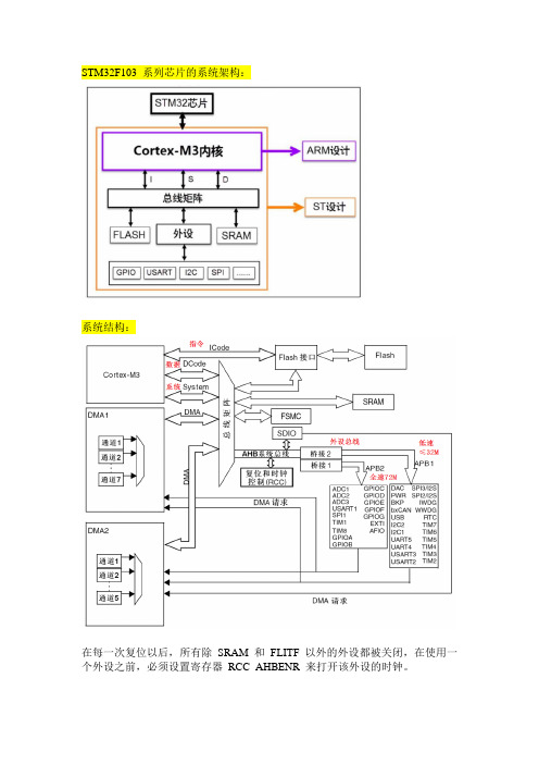
STM32F103 系列芯片的系统架构:系统结构:在每一次复位以后,所有除SRAM 和FLITF 以外的外设都被关闭,在使用一个外设之前,必须设置寄存器RCC_AHBENR 来打开该外设的时钟。
GPIO 输入输出,外部中断,定时器,串口。
理解了这四个外设,基本就入门了一款MCU。
时钟控制RCC:-4~16M 的外部高速晶振-内部8MHz 的高速RC 振荡器-内部40KHz低速RC 振荡器,看门狗时钟-内部锁相环(PLL,倍频),一般系统时钟都是外部或者内部高速时钟经过PLL 倍频后得到- 外部低速32.768K 的晶振,主要做RTC 时钟源ARM存储器映像:数据字节以小端格式存放在存储器中。
一个字里的最低地址字节被认为是该字的最低有效字节,而最高地址字节是最高有效字节。
存储器映像与寄存器映射:ARM 存储器映像4GB0X0000 00000X1FFF FFFF0X2000 00000X3FFF FFFF0X4000 00000X5FFF FFFF寄存器名称相对外设基地址的偏移值编号位表读写权限寄存器位功能说明使用C语言封装寄存器:1、总线和外设基地址封装利用地址偏移(1)定义外设基地址(Block2 首地址)(2)定义APB2总线基地址(相对外设基地址偏移固定)(3)定义GPIOX外设基地址(相对APB2总线基地址偏移固定)(4)定义GPIOX寄存器地址(相对GPIOX外设基地址偏移固定)(5)使用 C 语言指针操作寄存器进行读/写//定义外设基地址#define PERIPH_BASE ((unsigned int)0x40000000) 1)//定义APB2 总线基地址#define APB2PERIPH_BASE (PERIPH_BASE + 0x00010000) 2)//定义GPIOC 外设基地址#define GPIOC_BASE (AHB1PERIPH_BASE + 0x0800) 3)//定义寄存器基地址这里以GPIOC 为例#define GPIOC_CRL *(unsigned int*)(GPIOC_BASE+0x00) 4)#define GPIOC_CRH *(unsigned int*)(GPIOC_BASE+0x04)#define GPIOC_IDR *(unsigned int*)(GPIOC_BASE+0x08)#define GPIOC_ODR *(unsigned int*)(GPIOC_BASE+0x0C)#define GPIOC_BSRR *(unsigned int*)(GPIOC_BASE+0x10)#define GPIOC_BRR *(unsigned int*)(GPIOC_BASE+0x14)#define GPIOC_LCKR *(unsigned int*)(GPIOC_BASE+0x18)//控制GPIOC 第0 管脚输出一个低电平5)GPIOC_BSRR = (0x01<<(16+0));//控制GPIOC 第0 管脚输出一个高电平GPIOC_BSRR = (0x01<<0);2、寄存器封装利用结构体、外设基地址和寄存器地址偏移typedef unsigned int uint32_t; /*无符号32 位变量*/typedef unsigned short int uint16_t; /*无符号16 位变量*//* GPIO 寄存器列表*/typedef struct{uint32_t CRL; /*GPIO 端口配置低寄存器地址偏移: 0x00 */uint32_t CRH; /*GPIO 端口配置高寄存器地址偏移: 0x04 */uint32_t IDR; /*GPIO 数据输入寄存器地址偏移: 0x08 */uint32_t ODR; /*GPIO 数据输出寄存器地址偏移: 0x0C */uint32_t BSRR; /*GPIO 位设置/清除寄存器地址偏移: 0x10 */uint32_t BRR; /*GPIO 端口位清除寄存器地址偏移: 0x14 */uint16_t LCKR; /*GPIO 端口配置锁定寄存器地址偏移: 0x18 */}GPIO_TypeDef;只要给结构体设置好首地址,就能把结构体内成员的地址确定下来,然后就能以结构体的形式访问寄存器。
红牛开发板stm32f103zet6用户手册
红牛开发板用户手册 CopyRight@20091.概述红牛STM32开发板是以意法半导体 (ST)公司推出的基于ARM Cortex-M3系列最高配置芯片STM32F103ZE为核心组成。
板上资源:●CPU:STM32F103ZET6;(LQFP144脚,片上集成512K flash、64KRAM、12Bit ADC、DAC、PWM、CAN、USB、SDIO、FSMC等资源)●板上外扩512K SRAM, 2M NOR FLASH (板上支持最大1024kSRAM,16M的NOR FLASH)满足大容量数据采集、处理及分析要求●板上外扩128M或256M NAND FLASH(标配128M)满足彩屏上丰富的图片存储、数据表格存储,文件管理等应用● 搭配2.8寸TFT真彩触摸屏模块或3.2寸TFT真彩触摸屏模块(由用户选择),FSMC控制,彩屏模块上配置RSM1843(ADS7843、TSC2046脚对脚兼容)触摸控制器芯片,支持一个SD卡(SPI方式)可用于存储图片,支持一个AT45DBxxx 的DATA FLASH(可用于存储汉字库)● 一路CAN通信接口,驱动器芯片SN65VHD230● 两路RS232接口● 一路RS485通信接口● 一个SD卡座SDIO控制方式● 一个I2C存储器接口,标配24LC02(EEPROM)● 一个SPI存储器接口,标配AT45DB161D(DATA FLASH)● 一路ADC调节电位器输入● 三路ADC输入接线端子引出● 两路PWM输出接线端子引出● 两路DAC输出接线端子引出● 一个蜂鸣器、五个用户LED灯、一个电源指示灯,一个USB通信指示灯,● 四个用户按键,一个系统复位按键● 电源选择跳线,支持外接5V 电源供电,USB 供电或JLINK 供电 ● 板子规格尺寸:13CM X 10CM● 所有I/O 口通过2.54MM 标准间距引出,方便二次开发板上的全部硬件特性能快速帮助你评估STM32F103ZE 所有外设(USB 、motor control,、CAN,、SPI 、MicroSD card 、smartcard 、USART 、NOR Flash 、NAND flash 、 SRAM )和开发你自己的应用项目。
原子stm32f103zet6 晶振电容
原子stm32f103zet6 晶振电容The STM32F103ZET6 is a microcontroller from the STM32family manufactured by STMicroelectronics. One particular aspect related to this microcontroller is the crystal oscillator circuit and its corresponding capacitors, which are crucial for proper operation and reliable clock signal generation.In order to enable the crystal oscillator on theSTM32F103ZET6, you will need to connect two capacitors in parallel with the crystal. The value of these capacitors depends on the specific requirements of your crystal, so it is important to consult its datasheet for recommended values. Normally, crystals used with microcontrollers like the STM32F103ZET6 have a typical capacitance specified, which serves as a starting point.The function of these capacitors is to stabilize and adjust the oscillation frequency of the crystal. They form part of what is known as the load capacitance, which consists of both internal and external capacitances. The total loadcapacitance seen by the crystal should match its specified or recommended load capacitance value.It's worth noting that there are different types ofcrystals available on the market: parallel resonantcrystals and series resonant crystals. Each type has its own specific capacitor requirements. For example, parallel resonant crystals require two equal value capacitors connected in parallel with it, while series resonant crystals usually don't require any external capacitors.To choose suitable capacitors for your STM32F103ZET6crystal oscillator circuit, you can follow these general guidelines:1. Check the datasheet or specifications of your crystalfor its load capacitance requirement.2. If using a parallel resonant crystal, select two equal value capacitors within a close range of the recommended or specified load capacitance.3. Series resistance (ESR) characteristics of electrolytic capacitors should be considered if used.4. Ceramic capacitors are commonly used due to their low cost and various available options.5. Experiment with different capacitor values around the recommended or specified load capacitance to fine-tune the oscillator frequency if necessary.Remember that accurate clock signals are crucial for the proper functioning of a microcontroller, so it is important to pay attention to the crystal oscillator circuit and its associated capacitors. By choosing appropriate capacitors for your specific crystal, you will ensure stable and reliable clock signal generation for your STM32F103ZET6.我的问题是:原子stm32f103zet6 晶振电容STM32F103ZET6是STMicroelectronics生产的STM32系列微控制器之一。
基于STM32F103ZET6智能梯控系统的设计与实现
实验结果表明,该火灾自动报警系统具有较高的可靠性和有效性。在模拟火 灾的实验中,系统能够迅速检测到火灾并发出报警信号,同时启动声光报警装置 提醒人员采取措施。此外,系统在连续工作24小时后仍能保持稳定的性能表现, 误报率较低,可以满足一般场所的火灾监测需求。
总结起来,基于STM32F103ZET6单片机的火灾自动报警系统设计具有实时监 测、及时报警、智能化等特点,能够预防和减少火灾的发生,提高人们的生活质 量。该系统已通过实验验证了其可靠性和有效性,具有一定的应用价值。未来研 究方向可以包括优化传感器性能、提高系统稳定性、实现更多智能化功能等。希 望能为相关领域的研究和实践提供有益的参考和借鉴。
在调试过程中,我们需要注意以下问题: 1、检查硬件连接的正确性,确保各个设备都能正常工作;
2、观察电机驱动器的运行状态,确保电机运转正常; 3、检查传感器数据采集的准确性和实时性,以便及时作出避障决策;
4、优化电池续航能力,延长智能小车运行时间; 5、根据实际运行情况调整程序参数,提高智能小车的鲁棒性。
引言
随着全球能源危机的加剧和环保意识的提高,电动汽车及其相关技术得到了 越来越广泛的应用。作为电动汽车的核心部件,动力电池的性能和管理直接影响 到整个系统的运行。因此,设计一种高效、可靠、智能的动力电池管理系统显得 尤为重要。本次演示将基于STM32F103ZET6微控制器,探讨动力电池管理系统的 设计及实现方法。
关键词
动力电池管理系统,STM32F103ZET6,电池管理芯片,传感器,执行器,电 路设计,软件开发。
系统设计
动力电池管理系统主要由电池组、电池管理芯片、传感器、执行器以及电路 设计等部分组成。电池组是系统的核心,由多个单体电池通过串并联组成。 STM32F103ZET6微控制器作为电池管理芯片的主要控制单元,负责电池组的充放 电管理、温度监测、安全保护等功能。
MEMORY存储芯片STM32F103ZET6中文规格书
DS5792 Rev 13Absolute maximum ratingsStresses above the absolute maximum ratings listed in Table 7: Voltage characteristics , Table 8: Current characteristics , and Table 9: Thermal characteristics may cause permanent damage to the device. These are stress ratings only and functional operation of the device at these conditions is not implied. Exposure to maximum rating conditions for extended periods may affect device reliability.Table 7. Voltage characteristicsSymbol RatingsMin Max UnitV DD –V SS External main supply voltage (including V DDAand V DD)(1)1.All main power (V DD , V DDA ) and ground (V SS , V SSA ) pins must always be connected to the external powersupply, in the permitted range.–0.3 4.0V V IN (2)2.V IN maximum must always be respected. Refer to Table 8: Current characteristics for the maximumallowed injected current values.Input voltage on five volt tolerant pin V SS − 0.3V DD + 4.0 Input voltage on any other pinV SS − 0.34.0|ΔV DDx |Variations between different V DD power pins -50mV |V SSX − V SS |Variations between all the different ground pins (3)3.Include V REF- pin.-50V ESD(HBM)Electrostatic discharge voltage (human body model)see Section 5.3.12:Absolute maximum ratings (electrical sensitivity)-Table 8. Current characteristicsSymbol RatingsMax.UnitI VDD Total current into V DD /V DDA power lines (source)(1)1.All main power (V DD , V DDA ) and ground (V SS , V SSA ) pins must always be connected to the external powersupply, in the permitted range.150mA I VSS Total current out of V SS ground lines (sink)(1)150I IO Output current sunk by any I/O and control pin 25Output current source by any I/Os and control pin − 25I INJ(PIN)(2)2.Negative injection disturbs the analog performance of the device. See note 3 below Table 62 on page 108.Injected current on five volt tolerant pins (3)3.Positive injection is not possible on these I/Os. A negative injection is induced by V IN <V SS . I INJ(PIN) mustnever be exceeded. Refer to Table 7: Voltage characteristics for the maximum allowed input voltage values.-5/+0Injected current on any other pin (4)4.A positive injection is induced by V IN >V DD while a negative injection is induced by V IN <V SS . I INJ(PIN) must never be exceeded. Refer to Table 7: Voltage characteristics for the maximum allowed input voltage values.± 5ΣI INJ(PIN)Total injected current (sum of all I/O and control pins)(5)5.When several inputs are submitted to a current injection, the maximum ΣI INJ(PIN) is the absolute sum of thepositive and negative injected currents (instantaneous values).± 25Electrical characteristics STM32F103xC, STM32F103xD, STM32F103xEDS5792 Rev 135.3 Operating conditions5.3.1General operating conditionsTable 9. Thermal characteristicsSymbol RatingsValue Unit T STG Storage temperature range –65 to +150°C T JMaximum junction temperature150°CTable 10. General operating conditionsSymbol ParameterConditionsMin Max Unitf HCLK Internal AHB clock frequency -0 72MHz f PCLK1Internal APB1 clock frequency -0 36f PCLK2Internal APB2 clock frequency -0 72V DDStandard operating voltage -2 3.6V V DDA (1)1.When the ADC is used, refer to Table 59: ADC characteristics .Analog operating voltage(ADC not used)Must be the same potential as V DD (2)2.It is recommended to power V DD and V DDA from the same source. A maximum difference of 300mVbetween V DD and V DDA can be tolerated during power-up and operation.2 3.6VAnalog operating voltage (ADC used)2.43.6V BATBackup operating voltage- 1.8 3.6V P DPower dissipation at T A = 85°C for suffix 6 or T A = 105°C for suffix 7(3)3.If T A is lower, higher P D values are allowed as long as T J does not exceed T J max (see Table 6.7: Thermalcharacteristics on page 132).LQFP144-666mW LQFP100-434LQFP64-444LFBGA100-500LFBGA144-500WLCSP64-400T AAmbient temperature for 6 suffix versionMaximum power dissipation -4085°C Low-power dissipation (4)4.In low-power dissipation state, T A can be extended to this range as long as T J does not exceed T J max (seeTable 6.7: Thermal characteristics on page 132).-40105Ambient temperature for 7 suffix versionMaximum power dissipation -40105°CLow-power dissipation (4)-40125T JJunction temperature range6 suffix version -40105°C7 suffix version-40125DS5792 Rev 13STM32F103xC, STM32F103xD, STM32F103xE Electrical characteristics5.3.2 Operating conditions at power-up / power-downThe parameters given in Table 11 are derived from tests performed under the ambienttemperature condition summarized in Table 10.5.3.3 Embedded reset and power control block characteristicsThe parameters given in Table 12 are derived from tests performed under ambient temperature and V DD supply voltage conditions summarized in Table 10.Table 11. Operating conditions at power-up / power-downSymbol ParameterConditionsMin Max Unit t VDDV DD rise time rate -0∞µs/VV DD fall time rate20∞Table 12. Embedded reset and power control block characteristicsSymbolParameterConditionsMin Typ Max UnitV PVDProgrammable voltage detector level selection PLS[2:0]=000 (rising edge) 2.1 2.18 2.26V PLS[2:0]=000 (falling edge)2 2.08 2.16PLS[2:0]=001 (rising edge) 2.19 2.28 2.37PLS[2:0]=001 (falling edge) 2.09 2.18 2.27PLS[2:0]=010 (rising edge) 2.28 2.38 2.48PLS[2:0]=010 (falling edge) 2.18 2.28 2.38PLS[2:0]=011 (rising edge)2.38 2.48 2.58PLS[2:0]=011 (falling edge) 2.28 2.38 2.48PLS[2:0]=100 (rising edge)2.47 2.58 2.69PLS[2:0]=100 (falling edge) 2.37 2.48 2.59PLS[2:0]=101 (rising edge) 2.57 2.68 2.79PLS[2:0]=101 (falling edge) 2.47 2.58 2.69PLS[2:0]=110 (rising edge) 2.66 2.78 2.9PLS[2:0]=110 (falling edge) 2.56 2.68 2.8PLS[2:0]=111 (rising edge) 2.76 2.883PLS[2:0]=111 (falling edge)2.66 2.78 2.9V PVDhyst (2)PVD hysteresis--100-mV V POR/PDR Power on/power down reset threshold Falling edge 1.8(1)1.The product behavior is guaranteed by design down to the minimum V POR/PDR value.1.88 1.96V Rising edge 1.84 1.922.0V PDRhyst (2)PDR hysteresis--40-mV T RSTTEMPO (2)2.Guaranteed by design.Reset temporization-12.54.5msElectrical characteristics STM32F103xC, STM32F103xD, STM32F103xEDS5792 Rev 13DS5792 Rev 13STM32F103xC, STM32F103xD, STM32F103xE Electrical characteristicsTable 14. Maximum current consumption in Run mode, code with data processingrunning from FlashSymbolParameterConditionsf HCLK Max (1)1.Guaranteed by characterization results.UnitT A = 85°CT A = 105°CI DDSupply current in Run modeExternal clock (2), all peripherals enabled 2.External clock is 8 MHz and PLL is on when f HCLK > 8 MHz.72 MHz 6970mA48 MHz5050.536 MHz 3939.524 MHz272816 MHz2020.58 MHz 1111.5External clock (2), all peripherals disabled 72 MHz 3737.548 MHz2828.536 MHz 2222.524 MHz16.51716 MHz 12.5138 MHz88Table 15. Maximum current consumption in Run mode, code with data processingrunning from RAMSymbolParameterConditionsf HCLK Max (1)1.Guaranteed by characterization results at V DD max, f HCLK max.UnitT A = 85°CT A = 105°CI DDSupply current in Run modeExternal clock (2), all peripherals enabled 2.External clock is 8 MHz and PLL is on when f HCLK > 8 MHz.72 MHz 6667mA48 MHz43.545.536 MHz 333524 MHz2324.516 MHz16188 MHz 910.5External clock (2), all peripherals disabled 72 MHz 3333.548 MHz2323.536 MHz 1818.524 MHz1313.516 MHz 1010.58 MHz66.5。