iw1规格书中文版
MW6S004NT1;中文规格书,Datasheet资料

RF Power Field Effect TransistorN-Channel Enhancement-Mode Lateral MOSFETDesigned for Class A or Class AB base station applications with frequencies up to 2000 MHz. Suitable for analog and digital modulation and multicarrier amplifier applications.•Typical Two-Tone Performance @ 1960 MHz, 28 Volts, I DQ = 50 mA, P out = 4 Watts PEP Power Gain — 18 dB Drain Efficiency — 33%IMD — -34 dBc•Typical Two-Tone Performance @ 900 MHz, 28 Volts, I DQ = 50 mA, P out = 4 Watts PEP Power Gain — 19 dB Drain Efficiency — 33%IMD — -39 dBc•Capable of Handling 5:1 VSWR, @ 28 Vdc, 1960 MHz, 4 Watts CW Output Power Features•Characterized with Series Equivalent Large-Signal Impedance Parameters •On-Chip RF Feedback for Broadband Stability •Integrated ESD Protection •RoHS Compliant•In Tape and Reel. T1 Suffix = 1000 Units per 12 mm, 7 inch Reel.Table 1. Maximum RatingsRatingSymbol Value Unit Drain-Source Voltage V DSS -0.5, +68Vdc Gate-Source Voltage V GS -0.5, +12Vdc Storage Temperature Range T stg -65 to +150°C Operating Junction TemperatureT J150°CTable 2. Thermal CharacteristicsCharacteristicSymbol Value (1,2)Unit Thermal Resistance, Junction to CaseCase Temperature 76°C, 4 W PEP , Two-Tone Case Temperature 79°C, 4 W CWR θJC8.88.5°C/WTable 3. ESD Protection CharacteristicsTest MethodologyClass Human Body Model (per JESD22-A114)1C (Minimum)Machine Model (per EIA/JESD22-A115) A (Minimum)Charge Device Model (per JESD22-C101)IV (Minimum)1.MTTF calculator available at /rf. Select Software & Tools/Development Tools/Calculators to access MTTF calculators by product.2.Refer to AN1955, Thermal Measurement Methodology of RF Power Amplifiers. Go to /rf. Select Documentation/Application Notes - AN1955.Document Number: MW6S004NRev. 4, 6/2009Freescale Semiconductor Technical DataMW6S004NT1Table 4. Moisture Sensitivity LevelTest MethodologyRating Package Peak TemperatureUnit Per JESD 22-A113, IPC/JEDEC J-STD-0203260°CTable 5. Electrical Characteristics (T A = 25°C unless otherwise noted)CharacteristicSymbolMinTypMaxUnitOff CharacteristicsZero Gate Voltage Drain Leakage Current (V DS = 68 Vdc, V GS = 0 Vdc)I DSS ——10μAdc Zero Gate Voltage Drain Leakage Current (V DS = 28 Vdc, V GS = 0 Vdc)I DSS ——10μAdc Gate-Source Leakage Current (V GS = 5 Vdc, V DS = 0 Vdc)I GSS——500nAdcOn CharacteristicsGate Threshold Voltage(V DS = 10 Vdc, I D = 50 mAdc)V GS(th) 1.22 2.7Vdc Gate Quiescent Voltage(V DS = 28 Vdc, I D = 50 mAdc)V GS(Q)— 2.7—Vdc Fixture Gate Quiescent Voltage (1)(V DD = 28 Vdc, I D = 50 mAdc, Measured in Functional Test)V GG(Q) 2.23 4.2Vdc Drain-Source On-Voltage(V GS = 10 Vdc, I D = 50 mAdc)V DS(on)—0.270.37VdcDynamic CharacteristicsReverse Transfer Capacitance(V DS = 28 Vdc ± 30 mV(rms)ac @ 1 MHz, V GS = 0 Vdc)C rss —21—pF Output Capacitance(V DS = 28 Vdc ± 30 mV(rms)ac @ 1 MHz, V GS = 0 Vdc)C oss —25—pF Input Capacitance(V DS = 28 Vdc, V GS = 0 Vdc ± 30 mV(rms)ac @ 1 MHz)C iss—30—pFFunctional Tests (In Freescale Test Fixture, 50 ohm system) V DD = 28 Vdc, I DQ = 50 mA, P out = 4 W PEP , f1 = 1960 MHz, f2 = 1960.1 MHz, Two-Tone Test Power Gain G ps 16.51820dB Drain EfficiencyηD 2833—%Intermodulation Distortion IMD —-34-28dBc Input Return LossIRL—-12-10dBTypical Performance (In Freescale 900 MHz Demo Board, 50 ohm system) V DD = 28 Vdc, I DQ = 50 mA, P out = 4 W PEP , f = 900 MHz, Two-Tone Test, 100 kHz Tone Spacing Power Gain G ps —19—dB Drain EfficiencyηD —33—%Intermodulation Distortion IMD —-39—dBc Input Return LossIRL—-12—dB1.V GG = 11/10 x V GS(Q). Parameter measured on Freescale Test Fixture, due to resistive divider network on the board. Refer to Test Circuit Schematic.MW6S004NT1Figure 1. MW6S004NT1 Test Circuit SchematicZ70.210″ x 1.220″ Microstrip Z80.054″ x 0.680″ Microstrip Z90.054″ x 0.260″ Microstrip Z100.025″ x 0.930″ MicrostripPCBArlon CuClad 250GX-0300-55-22, 0.020″, εr = 2.5Z10.054″ x 0.430″ Microstrip Z20.054″ x 0.137″ Microstrip Z30.580″ x 0.420″ Microstrip Z40.580″ x 0.100″ Microstrip Z50.025″ x 0.680″ Microstrip Z60.210″ x 0.100″ MicrostripV SUPPLYTable 6. MW6S004NT1 Test Circuit Component Designations and ValuesPartDescriptionPart Number Manufacturer C1100 nF Chip Capacitor CDR33BX104AKYS Kemet C2, C3, C6, C79.1 pF Chip Capacitors ATC100B9R1CT500XT ATC C4, C510 μF, 50 V Chip Capacitors GRM55DR61H106KA88B Murata C810 μF, 35 V Tantalum Chip Capacitor T490D106K035AT Kemet R1 1 k Ω, 1/4 W Chip Resistor CRCW12061001FKEA Vishay R210 k Ω, 1/4 W Chip Resistor CRCW12061002FKEA Vishay R310 Ω, 1/4 W Chip ResistorCRCW120610R0FKEAVishayMW6S004NT1Figure 2. MW6S004NT1 Test Circuit Component LayoutMW6S004NT1TYPICAL CHARACTERISTICS1420191716G p s , P O W E R G A I N (d B )100.1TWO−TONE SPACING (MHz)1100Figure 6. Intermodulation Distortion Productsversus Tone Spacing 26P in , INPUT POWER (dBm)1618222414Figure 7. Pulsed CW Output Power versusInput PowerI M D , I N T E R M O D U L A T I O N D I S T O R T I O N (d B c )181520MW6S004NT1TYPICAL CHARACTERISTICSA C P R (dB )−70P out , OUTPUT POWER (WATTS) AVG.50−2040−3030−4020−5010−600.01110Figure 8. Single-Carrier CDMA ACPR, Power Gainand Drain Efficiency versus Output PowerP out , OUTPUT POWER (WATTS) CWFigure 10. Power Gain versus Output Power 7151906171618234G p s , P O W E R G A I N (d B )1800−250f, FREQUENCY (MHz)Figure 11. Broadband Frequency Response−5−10−15−20210020502000195019001850S 11 (d B )851ηD , D R A I N E F F I C I E N C Y (%), G p s , P O W E R G A I N (d B )0.118.517.516.515.5MW6S004NT1TYPICAL CHARACTERISTICS25010790T J , JUNCTION TEMPERATURE (°C)Figure 12. MTTF versus Junction TemperatureThis above graph displays calculated MTTF in hours when the device is operated at V DD = 28 Vdc, P out = 4 W PEP, and ηD = 33%.MTTF calculator available at /rf. Select Software & Tools/Development Tools/Calculators to access MTTF calculators by product.106105104110130150170190M T T F (H O U R S )210230MW6S004NT1f = 1930 MHzZ o = 10 ΩZ loadZ sourcef = 1990 MHzf = 1930 MHzf = 1990 MHzV DD = 28 Vdc, I DQ = 50 mA, P out = 4 W PEPfMHzZ sourceWZ loadW1930 1.96 - j5.348.78 + j6.961960 1.89 - j5.108.93 + j7.461990 1.82 - j4.859.11 + j7.97Z source=Test circuit impedance as measured fromgate to ground.Z load=Test circuit impedance as measured fromdrain to ground.Z source Z loadOutputMatchingNetworkFigure 13. Series Equivalent Source and Load ImpedanceMW6S004NT1Table 7. Common Source Scattering Parameters (V DD = 28 V, 50 ohm system)I DQ = 50 mAf MH S 11S 21S 12S 22MHz |S 11|∠φ|S 21|∠φ|S 12|∠φ|S 22|∠φ5000.649-116.3407.902105.4200.056-73.7500.548-33.5705500.695-121.6807.50298.7900.053-80.5700.593-41.4806000.733-126.5607.11192.3800.049-87.0100.632-48.8906500.770-131.340 6.69986.2900.045-93.2800.669-56.0007000.800-135.740 6.30280.4500.041-99.1200.701-62.8107500.827-140.030 5.92274.8500.038-104.8500.727-69.2908000.848-143.950 5.55269.6300.035-110.1100.750-75.3508500.866-147.690 5.22064.5800.032-115.2200.770-81.1309000.882-151.140 4.89159.9700.029-119.9600.786-86.5709500.895-154.560 4.59755.4900.026-124.7900.800-91.73010000.907-157.590 4.31551.2400.024-129.0900.813-96.66010500.916-160.540 4.06047.1700.022-133.3700.824-101.34011000.923-163.310 3.81943.3400.020-137.4600.833-105.79011500.929-165.930 3.60139.6500.018-141.4400.840-110.05012000.935-168.430 3.39836.1100.017-145.3300.847-114.17012500.938-170.770 3.21032.7400.015-149.5400.851-118.06013000.942-173.030 3.03629.4900.014-153.4300.856-121.88013500.945-175.140 2.87526.3600.013-157.4600.859-125.52014000.948-177.170 2.72823.3300.012-161.9100.863-129.02014500.951-179.090 2.59020.4400.011-166.1800.866-132.39015000.953179.030 2.46417.6400.010-170.6300.869-135.65015500.954177.270 2.34714.9200.009-174.8900.872-138.76016000.955175.570 2.24012.3200.008179.9500.875-141.75016500.956173.980 2.1399.7400.008173.9200.877-144.65017000.957172.350 2.0477.2500.007167.7100.880-147.48017500.957170.800 1.958 4.8100.007161.8100.882-150.18018000.958169.340 1.879 2.4400.006155.3700.884-152.76018500.959167.920 1.8060.2600.006148.9400.886-155.23019000.959166.510 1.736-1.9800.005142.6300.887-157.58019500.960165.200 1.668-4.3100.005136.7400.888-160.05020000.959163.800 1.611-6.2400.005129.9100.890-162.07020500.959162.420 1.555-8.2900.005123.8100.891-164.19021000.958161.170 1.504-10.2700.005118.2000.892-166.14021500.958159.840 1.456-12.2100.005112.7400.893-168.06022000.957158.560 1.412-14.1300.005108.4600.894-169.84022500.957157.160 1.372-16.0100.005103.8400.896-171.61023000.955155.870 1.334-17.8700.00599.3100.896-173.26023500.954154.510 1.300-19.7000.00595.3600.897-174.83024000.953153.120 1.268-21.5100.00591.0300.898-176.39024500.953151.7301.238-23.2500.00587.4600.899-177.840MW6S004NT1Table 7. Common Source Scattering Parameters (V DD = 28 V, 50 ohm system) (continued)I DQ = 50 mAf MH S 11S 21S 12S 22MHz |S 11|∠φ|S 21|∠φ|S 12|∠φ|S 22|∠φ25000.952150.340 1.211-25.1200.00684.1600.899-179.27025500.950149.010 1.187-26.9200.00680.7800.897179.42026000.949147.380 1.166-28.6500.00677.8800.897178.12026500.948145.920 1.144-30.4200.00774.6700.898176.84027000.944144.200 1.121-32.3100.00771.3600.896175.48027500.944142.790 1.105-34.2300.00767.9800.897174.06028000.943141.020 1.088-36.0000.00763.9500.897172.93028500.941139.410 1.073-37.8700.00761.2300.896171.63029000.940137.640 1.058-39.7600.00859.8100.896170.33029500.938135.900 1.045-41.6800.00858.2800.896169.04030000.937133.8601.032-43.6100.00856.7400.895167.510分销商库存信息: FREESCALEMW6S004NT1。
FPGA可编程逻辑器件芯片XC2V1000-6FGG256I中文规格书
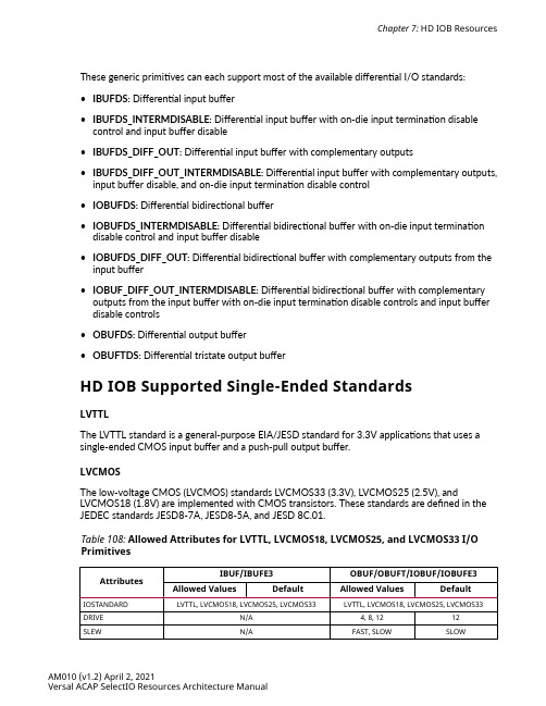
These generic primitives can each support most of the available differential I/O standards:•IBUFDS: Differential input buffer•IBUFDS_INTERMDISABLE: Differential input buffer with on-die input termination disable control and input buffer disable•IBUFDS_DIFF_OUT: Differential input buffer with complementary outputs•IBUFDS_DIFF_OUT_INTERMDISABLE: Differential input buffer with complementary outputs, input buffer disable, and on-die input termination disable control•IOBUFDS: Differential bidirectional buffer•IOBUFDS_INTERMDISABLE: Differential bidirectional buffer with on-die input termination disable control and input buffer disable•IOBUFDS_DIFF_OUT: Differential bidirectional buffer with complementary outputs from the input buffer•IOBUF_DIFF_OUT_INTERMDISABLE: Differential bidirectional buffer with complementary outputs from the input buffer with on-die input termination disable controls and input buffer disable controls•OBUFDS: Differential output buffer•OBUFTDS: Differential tristate output bufferHD IOB Supported Single-Ended StandardsLVTTLThe LVTTL standard is a general-purpose EIA/JESD standard for 3.3V applications that uses a single-ended CMOS input buffer and a push-pull output buffer.LVCMOSThe low-voltage CMOS (LVCMOS) standards LVCMOS33 (3.3V), LVCMOS25 (2.5V), and LVCMOS18 (1.8V) are implemented with CMOS transistors. These standards are defined in the JEDEC standards JESD8-7A, JESD8-5A, and JESD 8C.01.Table 108: Allowed Attributes for LVTTL, LVCMOS18, LVCMOS25, and LVCMOS33 I/O PrimitivesAttributesIBUF/IBUFE3OBUF/OBUFT/IOBUF/IOBUFE3 Allowed Values Default Allowed Values DefaultIOSTANDARD LVTTL, LVCMOS18, LVCMOS25, LVCMOS33LVTTL, LVCMOS18, LVCMOS25, LVCMOS33 DRIVE N/A4, 8, 1212SLEW N/A FAST, SLOW SLOWChapter 7: HD IOB ResourcesSSTLSSTL18_I is defined by the JEDEC standard JESD8-15, and is used for DDR2 SDRAM interfaces.For some topologies (such as short, point-to-point interfaces), the class-I driver can result in reduced overshoot and better signal integrity.HSTLThe high-speed transceiver logic (HSTL) HSTL_I_18 (1.8V) standard is a general-purpose high-speed bus standard as defined by the JEDEC standard JESD8-6.Table 109: Allowed Attributes for SSTL18_I and HSTL_I_18 I/O PrimitivesAttributesIBUF/IBUFE3OBUF/OBUFT IOBUF/IOBUFE3Allowed Values Default Allowed Value Default Allowed Values Default IOSTANDARDSSTL18_I, HSTL_I_18SSTL18_I, HSTL_I_18SSTL18_I, HSTL_I_18SLEWN/A FAST, SLOW SLOW FAST, SLOW SLOW ODT RTT_48,RTT_NONE RTT_NONE N/A RTT_48,RTT_NONERTT_NONE UNDEFINED Default IOSTANDARDWhen an IOSTANDARD is not defined by the user, the default assignment for the IOSTANDARD defaults to UNDEFINED. For a Versal ACAP design to complete implementation, a non-default IOSTANDARD must be defined with one of the valid I/O standards described in this section. The UNDEFINED standard acts as a placeholder to allow a design to complete the early stages or implementation.Single-Ended Input Buffer PrimitivesFigure 64: Single-Ended Input Buffer PrimitivesI OIBUFInput fromDevice Pad IBUF_INTERMDISABLEINTERMDISABLEOI Input fromDevice Pad IBUFDISABLEX21628-100720Table 110: IBUF and IBUF_INTERMDISABLE AttributesAttributeValues Description IOSTANDARDSee HD IOB Supported Standards Assigns an I/O standard to the E_IBUFDISABLE FALSE IBUFDISABLE is not supported in HD IOB and must be set to FALSE.(IBUF_INTERMDISABLE only)Table 111: IBUF and IBUF_INTERMDISABLE PortsPortI/O Description OOutput Buffer output representing the input path to the device.IInput Input port connection. Connect directly to top-level port in the design.IBUFDISABLE Input The IBUFDISABLE pin can disable the input buffer and force the O output to the internal logic to a logic High when the IBUFDISABLE signal is asserted High. (IBUF_INTERMDISABLE only)INTERMDISABLE InputIBUFDISABLE is not supported in HD IOB. (IBUF_INTERMDISABLE only)Single-Ended Bidirectional Buffer PrimitivesFigure 65: Single-Ended Bidirectional Buffer PrimitivesIOBUF_INTERMDISABLE IOIOBUFT I O IO X21629-092318Table 112: IOBUF, IOBUF_INTERMDISABLE AttributesAttributeValues Description DRIVE4, 8, 12Specifies the drive strength of the output.SLEWSLOW, FAST Specifies the slew rate of the output.IOSTANDARDSee HD IOB Supported Standards Assigns an I/O standard to the E_IBUFDISABLE FALSE IBUFDISABLE is not supported in HD IOB and must be set to FALSE.(IOBUF_INTERMDISABLE only)。
3.2V100AH电池组中文规格书

3.2其它事项
任何本规格书中未提及的事项,须经双方协商确定。
3.3.保质期及产品责任
保质期是从出厂日期开始起6个月
5.电芯操作注意事项
由于电池内部电芯属于软包装,为保证电芯的性能不受伤害,必须小心对电芯进行操作。
(7)用于上述测试的电池必须是新交货的电池,最迟是在一个月前交货,除非另有规定。
电池其他事项
1.外观检查
不允许有任何影响电池性能的外观缺陷,如裂纹、裂缝、泄漏等。
2.标准测试环境
除非特别说明,本规格书中所有测试均在以下环境条件下进行:
温度:25±5℃
湿度:65±20﹪RH
3.储存及其它事项
3.1长期储存
8.
充电时间
标准充电:7.0h(参考值)
快速充电:4.0h(参考值)
9.
最大充电电流
1.0 C
10.
最大放电电流
20C
11.
放电截至电压
2.0 V
12.
工作温度
充电:0°C ~ 45°C
放电:-20°C ~60°C
13.
储存温度
-10°C~45°C
14.
储存湿度
<85﹪
15.
电池重量
约:2.8Kg
5.电池性能
2
恒定湿热性能
搁置后放电容量/标称容量×100%>60%
电池外观无明显变形、无腐蚀、不冒烟、不爆炸、
电池标准充电后,置于温度为40℃±5℃,相对湿度为95%的恒温恒湿箱中,搁置168h后,取出电池搁置2h。观察电池外观变化。然后以0.2C5A放电至2.0V测量电池最终容量。
电感规格书模板

3.ELECTRCAL CHARACTERISTICS:(电气特性 )
3.1 ,TEST INDUCTANCE, ,DCR. (電感,直流電阻測試). TEST INSTRUMENT(測試儀器):CH3250 CH502 TEST CONDITION (測試條件):1KHz 0.25V
WINDING(绕组) N1(1 --- 2) DIAMETER AND TYPE (线径及线种) 2UEW 1.2*4 TURNS (圈 数) 5.5TS WINDING INDUCTANCE DCR METHOD(绕线方 (电感) (直流电阻) 式) 3.4uH+10% 135mΩ 疏绕满层
2.SCHMATIC:(线路图特 bb 比 // 大 p: tt h
TRIPLEWIRE (三层绝缘线) HEAT TUBE (热缩套管) VARNISH (凡立水) 蓝 菱 长 园 杰地 CB-HFT Φ3.0mm 468-2FC G-9008 CU EPOXY (环氧树脂胶) 固 德 德 昌 COPPER (铜 箔) 0.025*20MM
NO 1 2 3 4 5 6 7 8 9 10 11 ITEM(品名) BSAE(底坐) CORE(磁芯) PCB(隔板) WIRE (漆包线) TAPE(胶带) MATERAL(材质) FR-5 A10 R10K FR-1 2UEW #1350F-1 TRW-B SPECIFICATION(规格型号) BASE-002(6P),PIN距=7.0,排距=17.6 CORE,T22*14*8+C,A10,AL=7230+/-25% 13MM*10MM*2.0MM 0.2MM,0.3MM 15MM SUPPIER(供应商) 合 进 越 峰/伸 勇 福 宁 太平洋 3M
eta6954中文规格书

eta6954中文规格书一、引言eta6954是一种具有高效能和可靠性的设备,本文将详细介绍其规格和功能。
eta6954广泛应用于工业控制、通信设备和电子产品等领域,其规格书对于了解和选择该设备具有重要意义。
二、外观和尺寸eta6954外观采用工业级塑料外壳,尺寸为100mm×50mm×20mm,重量为100克。
设备外壳经过防尘、防水和抗震设计,能够适应各种恶劣环境条件。
三、工作电压和功耗eta6954工作电压范围为3.3V至5V,功耗低于1瓦。
该设备采用先进的节能技术,能够在保证性能的同时降低能量消耗,提高工作效率。
四、通信接口eta6954提供多种通信接口,包括RS232、RS485、以太网和USB接口。
用户可以根据实际需求选择合适的接口进行数据传输和控制。
通信速率可达到115200bps,能够满足高速数据传输的需求。
五、输入输出eta6954具有多个输入输出端口,包括数字输入、模拟输入、数字输出和模拟输出。
数字输入端口支持多种信号类型,如开关量、脉冲信号等。
模拟输入端口具有高精度和低噪声特性,能够准确采集模拟信号。
数字输出端口能够输出各种控制信号,模拟输出端口能够输出精确的模拟信号。
六、数据存储和处理eta6954配备了大容量的存储器,能够存储大量的数据。
同时,该设备还具有处理数据的能力,能够对采集到的数据进行实时处理和分析。
用户可以根据需要选择合适的存储器容量和处理能力。
七、温度和湿度范围eta6954能够在广泛的温度范围内正常工作,温度范围为-40℃至85℃。
该设备还具有良好的抗湿性能,湿度范围为0%至95%。
因此,eta6954适用于各种温湿度要求较高的场合。
八、安全性和可靠性eta6954具有高度的安全性和可靠性,符合相关的国际安全标准。
该设备具备过电压、过电流和过热保护功能,能够有效保护设备和用户的安全。
此外,eta6954还具有良好的抗干扰能力,能够在复杂的电磁环境下正常工作。
FPGA可编程逻辑器件芯片EP1S60F1020I5N中文规格书

2
150 – 240 150 – 230 150 – 200 150 – 200 36°, 72°, 108°, 144°
3
180 – 300 180 – 290 180 – 250 180 – 250 45°, 90°,135°, 180°
4
240 – 370 240 – 350 240 – 310 240 – 310 30°, 60°, 90°,120°
Table 1–5. Stratix III I/O Pin Leakage Current (Note 1), (2)
Symbol
Parameter
Conditions
Min Typ Max Unit
II
Input Pin Leakage Current
VI = VCCIOMAX to 0 V
-10
Table 1–41. Stratix III IOE Programmable Delay (Note 1)
Fast Model
C2 C3 C4
C4L
I3 I4
I4L
Industrial Commercial
Parameter
Available Settings
Min Offset
(2)
VCCL = VCCL = VCCL = VCCL = VCCL = VCCL = VCCL = VCCL = VCCL = 1.1V 1.1V 1.1V 1.1V 0.9V 1.1V 1.1V 1.1V 0.9V Unit
Low overdrive current
Min Max Min Max Min Max Min Max Min Max
ISUSL
VIN>VIL (maximum)
LSZ1R;LSZ1E;LSZ1V;LSZ1D;LSZ1W;中文规格书,Datasheet资料
If you need detailed product information, or help choosing the right product for your application, see our Interactive Catalog . Use the Interactive Catalog to access the most complete and up-to-date information available.The Interactive Catalog provides an extensive collection of product specifications, application data, and technical literature that can be searched based on criteria you select.This PDF catalog information was published in November 2000.Sensing and Control Honeywell Inc.11 West Spring Street Freeport, IL 61032/sensingSensing and ControlInteractive Catalog...Click this icon to try the Interactive Catalog.Interactive Catalog Supplements Catalog PDFsHoneywell ɀ Sensing and Control ɀ1-800-537-6945 USA ɀ⍣1-815-235-6847 International ɀ1-800-737-3360 Canada Delrin Coil Rod Spring LSZ4009LSZ4014inch long. For 7MICRO SWITCH conduit sealing packets can be used with limit or enclosed switches.This includes the HDLS, Compact LS, ML,E6, V6, BAF1or OP series switches.The conduit sealing packets are not suitablefor use with explosion-proof switches.This tool kit is used if readjustment of switch-es is necessary when heads and/or contactdetermine replacement parts catalog listing. The list-ings with -7A, -7M, -7N, -8A, -8B and -8C are complete catalog listings.B. Example LSZ1AB. For fluorocarbon seal replacement heads add C. Example LSZ1AC.A50Honeywellɀ Sensing and Controlɀ1-800-537-6945 USAɀ⍣1-815-235-6847 Internationalɀ1-800-737-3360 Canadadetermine replacement parts catalog listing. The list-ings with -7A, -7M, -7N, -8A, -8B and -8C are complete catalog listings.**Includes actuator B. Example LSZ1AB. For fluorocarbon seal replacement heads add C. Example LSZ1AC.Honeywellɀ Sensing and Controlɀ1-800-537-6945 USAɀ⍣1-815-235-6847 Internationalɀ1-800-737-3360 Canada A51determine replacement parts catalog listing. The list-ings with -7A, -7M, -7N, -8A, -8B and -8C are complete catalog listings.tors add B between the fifth and sixth characters. Example: LSZ1K B HA. For fluorocarbon seals add C. Example LSZ1K C HA.A52Honeywellɀ Sensing and Controlɀ1-800-537-6945 USAɀ⍣1-815-235-6847 Internationalɀ1-800-737-3360 Canadadetermine replacement parts catalog listing. The list-ings with -7A, -7M, -7N, -8A, -8B and -8C are complete catalog listings.Example LSZ1AB. For fluorocarbon seal replace-ment heads add C. Example LSZ1AC.Honeywellɀ Sensing and Controlɀ1-800-537-6945 USAɀ⍣1-815-235-6847 Internationalɀ1-800-737-3360 Canada A53*Only partial listings are shown and necessary to determine replacement parts catalog listing. The list-ings with -7A, -7M, -7N, -8A, -8B and -8C are complete catalog listings.Note: Complete units consist of Columns 1and 2.‡For low temperature replacement head and actua-tors add B between the fifth and sixth characters.Example LSZ1K B HA. For fluorocarbon seals add C.Example LSZ1K C HA.A54HoneywellɀSensing and Controlɀ1-800-537-6945 USAɀ⍣1-815-235-6847 Internationalɀ1-800-737-3360 CanadaHoneywell ɀSensing and Control ɀ1-800-537-6945 USA ɀ⍣1-815-235-6847 International ɀ1-800-737-3360 Canada A55分销商库存信息:HONEYWELLLSZ1R LSZ1E LSZ1V LSZ1D LSZ1W LSZ1F LSZ3A LSZ1A LSZ1KHA LSZ1JGM LSZ1C LSZ1G。
W25Q128JVSIQ规格书_W25Q128JVSIQ中文资料_W25Q128JVSIQ Datasheet
Publication Release Date: May 02, 2017Revision D3V 128M-BITSERIAL FLASH MEMORY WITH DUAL/QUAD SPI- 1 -Table of Contents1. GENERAL DESCRIPTIONS ............................................................................................................. 42. FEATURES ....................................................................................................................................... 43.PACKAGE TYPES AND PIN CONFIGURATIONS ........................................................................... 5 3.1 Pin Configuration SOIC 208-mil ........................................................................................... 5 3.2 Pad Configuration WSON 6x5-mm/ 8x6-mm ....................................................................... 5 3.3 Pin Description SOIC 208-mil, WSON 6x5-mm / 8x6-mm ................................................... 5 3.4 Pin Configuration SOIC 300-mil ........................................................................................... 6 3.5 Pin Description SOIC 300-mil ............................................................................................... 6 3.6 Ball Configuration TFBGA 8x6-mm (5x5 or 6x4 Ball Array) ................................................. 7 3.7Ball Description TFBGA 8x6-mm ......................................................................................... 7 4. PIN DESCRIPTIONS ........................................................................................................................ 8 4.1 Chip Select (/CS) .................................................................................................................. 8 4.2 Serial Data Input, Output and IOs (DI, DO and IO0, IO1, IO2, IO3) ..................................... 8 4.3 Write Protect (/WP) .............................................................................................................. 8 4.4 HOLD (/HOLD) ..................................................................................................................... 8 4.5 Serial Clock (CLK) ................................................................................................................ 8 4.6Reset (/RESET) (8)5. BLOCK DIAGRAM ............................................................................................................................ 96.FUNCTIONAL DESCRIPTIONS ..................................................................................................... 10 6.1 Standard SPI Instructions ................................................................................................... 10 6.2 Dual SPI Instructions .......................................................................................................... 10 6.3 Quad SPI Instructions ......................................................................................................... 10 6.4 Software Reset & Hardware /RESET pin ........................................................................... 10 6.5Write Protection (11)6.5.1 Write Protect Features (11)7. STATUS AND CONFIGURATION REGISTERS ............................................................................ 12 7.1Status Registers (12)7.1.1 Erase/Write In Progress (BUSY) – Status Only ................................................................ 12 7.1.2 Write Enable Latch (WEL) – Status Only .......................................................................... 12 7.1.3 Block Protect Bits (BP2, BP1, BP0) – Volatile/Non-Volatile Writable ................................ 12 7.1.4 Top/Bottom Block Protect (TB) – Volatile/Non-Volatile Writable ....................................... 13 7.1.5 Sector/Block Protect Bit (SEC) – Volatile/Non-Volatile Writable ....................................... 13 7.1.6 Complement Protect (CMP) – Volatile/Non-Volatile Writable ............................................ 13 7.1.1 Status Register Protect (SRP, SRL) – Volatile/Non-Volatile Writable ............................... 14 7.1.2 Erase/Program Suspend Status (SUS) – Status Only . (15)Publication Release Date: May 02, 2017- 2 - Revision D7.1.3 Security Register Lock Bits (LB3, LB2, LB1) – Volatile/Non-Volatile OTP Writable .......... 15 7.1.4 Quad Enable (QE) – Volatile/Non-Volatile Writable .......................................................... 15 7.1.5 Write Protect Selection (WPS) – Volatile/Non-Volatile Writable ....................................... 16 7.1.6 Output Driver Strength (DRV1, DRV0) – Volatile/Non-Volatile Writable ........................... 16 7.1.7 Reserved Bits – Non Functional ........................................................................................ 16 7.1.8 W25Q128JV Status Register Memory Protection (WPS = 0, CMP = 0) ............................... 17 7.1.9 W25Q128JV Status Register Memory Protection (WPS = 0, CMP = 1) ............................... 18 7.1.10 W25Q128JV Individual Block Memory Protection (WPS=1) . (19)8. INSTRUCTIONS ............................................................................................................................. 20 8.1Device ID and Instruction Set Tables (20)8.1.1 Manufacturer and Device Identification ................................................................................ 20 8.1.2 Instruction Set Table 1 (Standard SPI Instructions)(1)........................................................... 21 8.1.3 Instruction Set Table 2 (Dual/Quad SPI Instructions) ........................................................... 22 Notes: (22)8.2 Instruction Descriptions (23)8.2.1 Write Enable (06h) ............................................................................................................... 23 8.2.2 Write Enable for Volatile Status Register (50h) .................................................................... 23 8.2.3 Write Disable (04h) ............................................................................................................... 24 8.2.4 Read Status Register-1 (05h), Status Register-2 (35h) & Status Register-3 (15h) .............. 24 8.2.5 Write Status Register-1 (01h), Status Register-2 (31h) & Status Register-3 (11h) .............. 25 8.2.6 Read Data (03h) ................................................................................................................... 27 8.2.7 Fast Read (0Bh) ................................................................................................................... 28 8.2.8 Fast Read Dual Output (3Bh) ............................................................................................... 29 8.2.9 Fast Read Quad Output (6Bh) .............................................................................................. 30 8.2.10 Fast Read Dual I/O (BBh) ................................................................................................... 31 8.2.11 Fast Read Quad I/O (EBh) ................................................................................................. 32 8.2.12 Set Burst with Wrap (77h) .................................................................................................. 34 8.2.13 Page Program (02h) ........................................................................................................... 35 8.2.14 Quad Input Page Program (32h) ........................................................................................ 36 8.2.15 Sector Erase (20h) ............................................................................................................. 37 8.2.16 32KB Block Erase (52h) ..................................................................................................... 38 8.2.17 64KB Block Erase (D8h) ..................................................................................................... 39 8.2.18 Chip Erase (C7h / 60h) ....................................................................................................... 40 8.2.19 Erase / Program Suspend (75h) ......................................................................................... 41 8.2.20 Erase / Program Resume (7Ah) ......................................................................................... 42 8.2.21 Power-down (B9h) .............................................................................................................. 43 8.2.22 Release Power-down / Device ID (ABh) ............................................................................. 44 8.2.23 Read Manufacturer / Device ID (90h) ................................................................................. 45 8.2.24 Read Manufacturer / Device ID Dual I/O (92h) ................................................................... 46 8.2.25 Read Manufacturer / Device ID Quad I/O (94h) ................................................................. 47 8.2.26 Read Unique ID Number (4Bh). (48)- 3 -8.2.27 Read JEDEC ID (9Fh) ........................................................................................................ 49 8.2.28 Read SFDP Register (5Ah) ................................................................................................ 50 8.2.29 Erase Security Registers (44h) ........................................................................................... 51 8.2.30 Program Security Registers (42h) ...................................................................................... 52 8.2.31 Read Security Registers (48h) ........................................................................................... 53 8.2.32 Individual Block/Sector Lock (36h) ..................................................................................... 54 8.2.33 Individual Block/Sector Unlock (39h) .................................................................................. 55 8.2.34 Read Block/Sector Lock (3Dh) ........................................................................................... 56 8.2.35 Global Block/Sector Lock (7Eh) .......................................................................................... 57 8.2.36 Global Block/Sector Unlock (98h) ....................................................................................... 57 8.2.37 Enable Reset (66h) and Reset Device (99h) . (58)9.ELECTRICAL CHARACTERISTICS (59)9.1 Absolute Maximum Ratings (1) ............................................................................................ 59 9.2 Operating Ranges............................................................................................................... 59 9.3 Power-Up Power-Down Timing and Requirements ............................................................ 60 9.4 DC Electrical Characteristics- ............................................................................................. 61 9.5 AC Measurement Conditions .............................................................................................. 62 9.6 AC Electrical Characteristics (6) ........................................................................................... 63 9.7 Serial Output Timing ........................................................................................................... 65 9.8 Serial Input Timing .............................................................................................................. 65 9.9/WP Timing ......................................................................................................................... 65 10. PACKAGE SPECIFICATIONS ........................................................................................................ 66 10.1 8-Pin SOIC 208-mil (Package Code S) .............................................................................. 66 10.2 16-Pin SOIC 300-mil (Package Code F) ............................................................................ 67 10.3 8-Pad WSON 6x5-mm (Package Code P) ......................................................................... 68 10.4 8-Pad WSON 8x6-mm (Package Code E) ......................................................................... 69 10.5 24-Ball TFBGA 8x6-mm (Package Code B, 5x5-1 ball array) ............................................ 70 10.624-Ball TFBGA 8x6-mm (Package Code C, 6x4 ball array) ............................................... 71 11. ORDERING INFORMATION .......................................................................................................... 72 11.1Valid Part Numbers and Top Side Marking (73)12. REVISION HISTORY (74)Publication Release Date: May 02, 2017- 4 - Revision D1. GENERAL DESCRIPTIONSThe W25Q128JV (128M-bit) Serial Flash memory provides a storage solution for systems with limited space, pins and power. The 25Q series offers flexibility and performance well beyond ordinary Serial Flash devices. They are ideal for code shadowing to RAM, executing code directly from Dual/Quad SPI (XIP) and storing voice, text and data. The device operates on a single 2.7V to 3.6V power supply with current consumption as low as 1µA for power-down. All devices are offered in space-saving packages.The W25Q128JV array is organized into 65,536 programmable pages of 256-bytes each. Up to 256 bytes can be programmed at a time. Pages can be erased in groups of 16 (4KB sector erase), groups of 128 (32KB block erase), groups of 256 (64KB block erase) or the entire chip (chip erase). The W25Q128JV has 4,096 erasable sectors and 256 erasable blocks respectively. The small 4KB sectors allow for greater flexibility in applications that require data and parameter storage. (See Figure 2.)The W25Q128JV supports the standard Serial Peripheral Interface (SPI), Dual/Quad I/O SPI: Serial Clock, Chip Select, Serial Data I/O0 (DI), I/O1 (DO), I/O2 and I/O3. SPI clock frequencies of W25Q128JV of up to 133MHz are supported allowing equivalent clock rates of 266MHz (133MHz x 2) for Dual I/O and 532MHz (133MHz x 4) for Quad I/O when using the Fast Read Dual/Quad I/O. These transfer rates can outperform standard Asynchronous 8 and 16-bit Parallel Flash memories.Additionally, the device supports JEDEC standard manufacturer and device ID and SFDP, and a 64-bit Unique Serial Number and three 256-bytes Security Registers.2. FEATURES∙ New Family of SpiFlash Memories – W25Q128JV: 128M-bit / 16M-byte – Standard SPI: CLK, /CS, DI, DO – Dual SPI: CLK, /CS, IO 0, IO 1 – Quad SPI: CLK, /CS, IO 0, IO 1, IO 2, IO 3 – Software & Hardware Reset (1) ∙ Highest Performance Serial Flash – 133MHz Single, Dual/Quad SPI clocks – 266/532MHz equivalent Dual/Quad SPI – 66MB/S continuous data transfer rate – Min. 100K Program-Erase cycles per sector – More than 20-year data retention ∙ Efficient “Continuous Read”– Continuous Read with 8/16/32/64-Byte Wrap– As few as 8 clocks to address memory– Allows true XIP (execute in place) operation ∙ Low Power, Wide Temperature Range– Single 2.7 to 3.6V supply– <1µA Power-down (typ.)– -40°C to +85°C operating range∙ Flexible Architecture with 4KB sectors – Uniform Sector/Block Erase (4K/32K/64K-Byte) – Program 1 to 256 byte per programmable page – Erase/Program Suspend & Resume ∙ Advanced Security Features – Software and Hardware Write-Protect – Power Supply Lock-Down – Special OTP protection – Top/Bottom, Complement array protection – Individual Block/Sector array protection – 64-Bit Unique ID for each device – Discoverable Parameters (SFDP) Register– 3X256-Bytes Security Registers with OTP locks – Volatile & Non-volatile Status Register Bits ∙ Space Efficient Packaging – 8-pin SOIC 208-mil– 16-pin SOIC 300-mil (additional /RESET pin) – 8-pad WSON 6x5-mm / 8x6-mm – 24-ball TFBGA 8x6-mm (6x4/5x5 ball array) – Contact Winbond for KGD and other options Note: 1. Hardware /RESET pin is only available on TFBGA or SOIC16 packages- 5 -3. PACKAGE TYPES AND PIN CONFIGURATIONS3.1 Pin Configuration SOIC 208-milFigure 1a. W25Q128JV Pin Assignments, 8-pin SOIC 208-mil (Package Code S)3.2 Pad Configuration WSON 6x5-mm/ 8x6-mmFigure 1b. W25Q128JV Pad Assignments, 8-pad WSON 6x5-mm/ 8x6-mm (Package Code P/E)3.3 Pin Description SOIC 208-mil, WSON 6x5-mm / 8x6-mmNotes:1. IO0 and IO1 are used for Standard and Dual SPI instructions2.IO0 – IO3 are used for Quad SPI instructions, /HOLD (or /RESET) function is only available for Standard/Dual SPI.Publication Release Date: May 02, 2017- 6 - Revision D3.4 Pin Configuration SOIC 300-milFigure 1c. W25Q128JV Pin Assignments, 16-pin SOIC 300-mil (Package Code F)3.5 Pin Description SOIC 300-milNotes:1. IO0 and IO1 are used for Standard and Dual SPI instructions.2. IO0 – IO3 are used for Quad SPI instructions, /HOLD (or /RESET) function is only available for Standard/Dual SPI.3. The /RESET pin is a dedicated hardware reset pin regardless of device settings or operation states. If the hardware reset function is not used, this pin can be left floating or connected to VCC in the system.3.6Ball Configuration TFBGA 8x6-mm (5x5 or 6x4 Ball Array)Figure 1d. W25Q128JV Ball Assignments, 24-ball TFBGA 8x6-mm (Package Code B/C)3.7Ball Description TFBGA 8x6-mmNotes:1.IO0 and IO1 are used for Standard and Dual SPI instructions2.IO0 – IO3 are used for Quad SPI instructions, /HOLD (or /RESET) function is only available for Standard/Dual SPI.3. The /RESET pin is a dedicated hardware reset pin regardless of device settings or operation states.If the hardware reset function is not used, this pin can be left floating or connected to VCC in the system- 7 -Publication Release Date: May 02, 2017- 8 - Revision D4. PIN DESCRIPTIONS4.1 Chip Select (/CS)The SPI Chip Select (/CS) pin enables and disables device operation. When /CS is high the device is deselected and the Serial Data Output (DO, or IO0, IO1, IO2, IO3) pins are at high impedance. When deselected, the devices power consumption will be at standby levels unless an internal erase, program or write status register cycle is in progress. When /CS is brought low the device will be selected, power consumption will increase to active levels and instructions can be written to and data read from the device. After power-up, /CS must transition from high to low before a new instruction will be accepted. The /CS input must track the VCC supply level at power-up and power-down (see “Write Protection” and Figure 58). If needed a pull-up resister on the /CS pin can be used to accomplish this.4.2 Serial Data Input, Output and IOs (DI, DO and IO0, IO1, IO2, IO3)The W25Q128JV supports standard SPI, Dual SPI and Quad SPI operation. Standard SPI instructions use the unidirectional DI (input) pin to serially write instructions, addresses or data to the device on the rising edge of the Serial Clock (CLK) input pin. Standard SPI also uses the unidirectional DO (output) to read data or status from the device on the falling edge of CLK.Dual and Quad SPI instructions use the bidirectional IO pins to serially write instructions, addresses or data to the device on the rising edge of CLK and read data or status from the device on the falling edge of CLK. Quad SPI instructions require the non-volatile Quad Enable bit (QE) in Status Register-2 to be set. When QE=1, the /WP pin becomes IO2 and the /HOLD pin becomes IO3.4.3 Write Protect (/WP)The Write Protect (/WP) pin can be used to prevent the Status Register from being written. Used in conjunction with the Status Register’s Block Protect (CMP, SEC, TB, BP2, BP1 and BP0) bits and Status Register Protect (SRP) bits, a portion as small as a 4KB sector or the entire memory array can be hardware protected. The /WP pin is active low.4.4 HOLD (/HOLD)The /HOLD pin allows the device to be paused while it is actively selected. When /HOLD is brought low, while /CS is low, the DO pin will be at high impedance and signals on the DI and CLK pins will be ignored (don’t care). When /HOLD is brought high, device operation can resume. The /HOLD function can be useful when multiple devices are sharing the same SPI signals. The /HOLD pin is active low. When the QE bit of Status Register-2 is set for Quad I/O, the /HOLD pin function is not available since this pin is used for IO3. See Figure 1a-c for the pin configuration of Quad I/O operation.4.5 Serial Clock (CLK)The SPI Serial Clock Input (CLK) pin provides the timing for serial input and output operations. ("See SPI Operations")4.6 Reset (/RESET)A dedicated hardware /RESET pin is available on SOIC-16 and TFBGA packages. When it’s driven low for a minimum period of ~1µS, this device will terminate any external or internal operations and return to its power-on state.Note: Hardware /RESET pin is available on SOIC-16 or TFBGA; please contact Winbond for this package.- 9 -5. BLOCK DIAGRAMFigure 2. W25Q128JV Serial Flash Memory Block Diagram6.FUNCTIONAL DESCRIPTIONS6.1Standard SPI InstructionsThe W25Q128JV is accessed through an SPI compatible bus consisting of four signals: Serial Clock (CLK), Chip Select (/CS), Serial Data Input (DI) and Serial Data Output (DO). Standard SPI instructions use the DI input pin to serially write instructions, addresses or data to the device on the rising edge of CLK. The DO output pin is used to read data or status from the device on the falling edge of CLK.SPI bus operation Mode 0 (0,0) and 3 (1,1) are supported. The primary difference between Mode 0 and Mode 3 concerns the normal state of the CLK signal when the SPI bus master is in standby and data is not being transferred to the Serial Flash. For Mode 0, the CLK signal is normally low on the falling and rising edges of /CS. For Mode 3, the CLK signal is normally high on the falling and rising edges of /CS.6.2Dual SPI InstructionsThe W25Q128JV supports Dual SPI operation when using instructions such as “Fast Read Dual Output (3Bh)” and “Fast Read Dual I/O (BBh)”. These instructions allow data to be transferred to or from the device at two to three times the rate of ordinary Serial Flash devices. The Dual SPI Read instructions are ideal for quickly downloading code to RAM upon power-up (code-shadowing) or for executing non-speed-critical code directly from the SPI bus (XIP). When using Dual SPI instructions, the DI and DO pins become bidirectional I/O pins: IO0 and IO1.6.3Quad SPI InstructionsThe W25Q128JV supports Quad SPI operation when using instructions such as “Fast Read Quad Output (6Bh)”,and “Fast Read Quad I/O (EBh). These instructions allow data to be transferred to or from the device four to six times the rate of ordinary Serial Flash. When using Quad SPI instructions, the DI and DO pins become bidirectional IO0 and IO1, with the additional I/O pins: IO2, IO3.6.4Software Reset & Hardware /RESET pinThe W25Q128JV can be reset to the initial power-on state by a software Reset sequence. This sequence must include two consecutive instructions: Enable Reset (66h) & Reset (99h). If the instruction sequence is successfully accepted, the device will take approximately 30µS (t RST)to reset. No instruction will be accepted during the reset period. For the SOIC-16 and TFBGA packages, W25Q128JV provides a dedicated hardware /RESET pin. Drive the /RESET pin low for a minimum period of ~1µS (tRESET*) will interrupt any on-going external/internal operations and reset the device to its initial power-on state. Hardware /RESET pin has higher priority than other SPI input signals (/CS, CLK, IOs).Note:1.Hardware /RESET pin is available on SOIC-16 or TFBGA; please contact Winbond for his package.2.While a faster /RESET pulse (as short as a few hundred nanoseconds) will often reset the device, a 1us minimum isrecommended to ensure reliable operation.3.There is an internal pull-up resistor for the dedicated /RESET pin on the SOIC-16 and TFBGA-24 package. If the reset functionis not needed, this pin can be left floating in the system.6.5Write ProtectionApplications that use non-volatile memory must take into consideration the possibility of noise and other adverse system conditions that may compromise data integrity. To address this concern, the W25Q128JV provides several means to protect the data from inadvertent writes.6.5.1Write Protect Features∙Device resets when VCC is below threshold∙Time delay write disable after Power-up∙Write enable/disable instructions and automatic write disable after erase or program∙Software and Hardware (/WP pin) write protection using Status Registers∙Additional Individual Block/Sector Locks for array protection∙Write Protection using Power-down instruction∙Lock Down write protection for Status Register until the next power-up∙One Time Program (OTP) write protection for array and Security Registers using Status Register** Note:This feature is available upon special order. Please contact Winbond for details.Upon power-up or at power-down, the W25Q128JV will maintain a reset condition while VCC is below the threshold value of V WI, (See Power-up Timing and Voltage Levels and Figure 43). While reset, all operations are disabled and no instructions are recognized. During power-up and after the VCC voltage exceeds V WI, all program and erase related instructions are further disabled for a time delay of t PUW. This includes the Write Enable, Page Program, Sector Erase, Block Erase, Chip Erase and the Write Status Register instructions. Note that the chip select pin (/CS) must track the VCC supply level at power-up until the VCC-min level and t VSL time delay is reached, and it must also track the VCC supply level at power-down to prevent adverse command sequence. If needed a pull-up resister on /CS can be used to accomplish this.After power-up the device is automatically placed in a write-disabled state with the Status Register Write Enable Latch (WEL) set to a 0. A Write Enable instruction must be issued before a Page Program, Sector Erase, Block Erase, Chip Erase or Write Status Register instruction will be accepted. After completing a program, erase or write instruction the Write Enable Latch (WEL) is automatically cleared to a write-disabled state of 0.Software controlled write protection is facilitated using the Write Status Register instruction and setting the Status Register Protect (SRP, SRL) and Block Protect (CMP, TB, BP[3:0]) bits. These settings allow a portion or the entire memory array to be configured as read only. Used in conjunction with the Write Protect (/WP) pin, changes to the Status Register can be enabled or disabled under hardware control. See Status Register section for further information. Additionally, the Power-down instruction offers an extra level of write protection as all instructions are ignored except for the Release Power-down instruction.The W25Q128JV also provides another Write Protect method using the Individual Block Locks. Each 64KB block (except the top and bottom blocks, total of 126 blocks) and each 4KB sector within the top/bottom blocks (total of 32 sectors) are equipped with an Individual Block Lock bit. When the lock bit is 0, the corresponding sector or block can be erased or programmed; when the lock bit is set to 1, Erase or Program commands issued to the corresponding sector or block will be ignored. When the device is powered on, all Individual Block Lock bits will be 1, so the entire memory array is protected from Erase/Program. An “Individual Block Unlock (39h)” instruction must be issued to unlock any specific sector or block.The WPS bit in Status Register-3 is used to decide which Write Protect scheme should be used. When WPS=0 (factory default), the device will only utilize CMP, SEC, TB, BP[2:0] bits to protect specific areas of the array; when WPS=1, the device will utilize the Individual Block Locks for write protection.。
半导体传感器ADUM1401BRWZ中文规格书
Data SheetADuM1400/ADuM1401/ADuM1402 Rev. L | Page 9 of 31 ParameterSymbol Min Typ Max Unit Test Conditions 90 Mbps (CRW Grade Only)V DD1 Supply CurrentI DD1 (90) 5 V/3 V Operation57 82 mA 45 MHz logic signal freq. 3 V/5 V Operation30 52 mA 45 MHz logic signal freq. V DD2 Supply CurrentI DD2 (90) 5 V/3 V Operation18 27 mA 45 MHz logic signal freq. 3 V/5 V Operation31 43 mA 45 MHz logic signal freq. ADuM1402 Total Supply Current, Four Channels 2DC to 2 MbpsV DD1 Supply CurrentI DD1 (Q) 5 V/3 V Operation1.52.1 mA DC to 1 MHz logic signal freq. 3 V/5 V Operation0.9 1.5 mA DC to 1 MHz logic signal freq. V DD2 Supply CurrentI DD2 (Q) 5 V/3 V Operation0.9 1.5 mA DC to 1 MHz logic signal freq. 3 V/5 V Operation1.52.1 mA DC to 1 MHz logic signal freq. 10 Mbps (BRW and CRW Grades Only)V DD1 Supply CurrentI DD1 (10) 5 V/3 V Operation5.6 7.0 mA 5 MHz logic signal freq. 3 V/5 V Operation3.04.2 mA 5 MHz logic signal freq. V DD2 Supply CurrentI DD2 (10) 5 V/3 V Operation3.04.2 mA 5 MHz logic signal freq. 3 V/5 V Operation5.6 7.0 mA 5 MHz logic signal freq. 90 Mbps (CRW Grade Only)V DD1 Supply CurrentI DD1 (90) 5 V/3 V Operation44 62 mA 45 MHz logic signal freq. 3 V/5 V Operation24 39 mA 45 MHz logic signal freq. V DD2 Supply CurrentI DD2 (90) 5 V/3 V Operation24 39 mA 45 MHz logic signal freq. 3 V/5 V Operation44 62 mA 45 MHz logic signal freq. For All ModelsInput CurrentsI IA , I IB , I IC , I ID , I E1, I E2 −10 +0.01 +10 µA 0 V ≤ V IA , V IB , V IC , V ID ≤ V DD1 or V DD2, 0 V ≤ V E1, V E2 ≤ V DD1 or V DD2 Logic High Input ThresholdV IH , V EH 5 V/3 V Operation2.0 V 3 V/5 V Operation1.6 V Logic Low Input ThresholdV IL , V EL 5 V/3 V Operation0.8 V 3 V/5 V Operation0.4 V Logic High Output VoltagesV OAH , V OBH , V OCH , V ODH (V DD1 or V DD2) − 0.1 (V DD1 or V DD2) V I Ox = −20 µA, V Ix = V IxH (V DD1 or V DD2) − 0.4(V DD1 or V DD2) − 0.2 V I Ox = −3.2 mA, V Ix = V IxH Logic Low Output Voltages V OAL , V OBL ,V OCL , V ODL 0.0 0.1V I Ox = 20 µA, V Ix = V IxL 0.04 0.1V I Ox = 400 µA, V Ix = V IxL0.2 0.4 V I Ox = 3.2 mA, V Ix = V IxLSWITCHING SPECIFICATIONSADuM1400ARW /ADuM1401ARW /ADuM1402ARWMinimum Pulse Width 3PW 1000 ns C L = 15 pF, CMOS signal levels Maximum Data Rate 41 Mbps C L = 15 pF, CMOS signal levels Propagation Delay 5t PHL , t PLH 50 70 100 ns C L = 15 pF, CMOS signal levels Pulse Width Distortion, |t PLH − t PHL |5PWD 40 ns C L = 15 pF, CMOS signal levels Change vs. Temperature11 ps/°C C L = 15 pF, CMOS signal levels Propagation Delay Skew 6t PSK 50 ns C L = 15 pF, CMOS signal levels Channel-to-Channel Matching 7t PSKCD /t PSKOD 50 ns C L = 15 pF, CMOS signal levels ADuM1400BRW /ADuM1401BRW /ADuM1402BRWMinimum Pulse Width 3PW 100 ns C L = 15 pF, CMOS signal levels Maximum Data Rate 410 Mbps C L = 15 pF, CMOS signal levelsPropagation Delay 5 t PHL , t PLH 15 35 50 ns C L = 15 pF, CMOS signal levelsData SheetADuM1400/ADuM1401/ADuM1402 Rev. L | Page 13 of 31ELECTRICAL CHARACTERISTICS—3 V, 125°C OPERATION 1 3.0 V ≤ V DD1 ≤ 3.6 V , 3.0 V ≤ V DD2 ≤ 3.6 V; all minimum/maximum specifications apply over the entire recommended operation range, unless otherwise noted; all typical specifications are at T A = 25°C, V DD1 = V DD2 = 3.0 V . These specifications apply to ADuM1400W , ADuM1401W , and ADuM1402W automotive grade versions. Table 5.ParameterSymbol Min Typ Max Unit Test Conditions DC SPECIFICATIONSInput Supply Current per Channel,QuiescentI DDI (Q) 0.26 0.31 mA Output Supply Current per Channel,QuiescentI DDO (Q) 0.11 0.14 mA ADuM1400W , Total Supply Current, FourChannels 2DC to 2 MbpsV DD1 Supply CurrentI DD1 (Q) 1.2 1.9 mA DC to 1 MHz logic signal freq. V DD2 Supply CurrentI DD2 (Q) 0.5 0.9 mA DC to 1 MHz logic signal freq. 10 Mbps (TRWZ Grade Only)V DD1 Supply CurrentI DD1 (10) 4.5 6.5 mA 5 MHz logic signal freq. V DD2 Supply CurrentI DD2 (10) 1.4 2.0 mA 5 MHz logic signal freq. ADuM1401W , Total Supply Current, Four Channels 2DC to 2 MbpsV DD1 Supply CurrentI DD1 (Q) 1.0 1.6 mA DC to 1 MHz logic signal freq. V DD2 Supply CurrentI DD2 (Q) 0.7 1.2 mA DC to 1 MHz logic signal freq. 10 Mbps (TRWZ Grade Only)V DD1 Supply CurrentI DD1 (10) 3.7 5.4 mA 5 MHz logic signal freq. V DD2 Supply CurrentI DD2 (10) 2.2 3.0 mA 5 MHz logic signal freq. ADuM1402W , Total Supply Current, FourChannels 2DC to 2 MbpsV DD1 or V DD2 Supply CurrentI DD1 (Q), I DD2 (Q) 0.9 1.5 mA DC to 1 MHz logic signal freq. 10 Mbps (TRWZ Grade Only)V DD1 or V DD2 Supply CurrentI DD1 (10), I DD2 (10) 3.0 4.2 mA 5 MHz logic signal freq. For All ModelsInput CurrentsI IA , I IB , I IC , I ID , I E1, I E2 −10 +0.01+10µA 0 V ≤ V IA , V IB , V IC , V ID ≤ V DD1 or V DD2, 0 V ≤ V E1, V E2 ≤ V DD1 or V DD2 Logic High Input ThresholdV IH , V EH 1.6 V Logic Low Input ThresholdV IL , V EL 0.4 V Logic High Output VoltagesV OAH , V OBH , V OCH , V ODH (V DD1 or V DD2) − 0.1 3.0 V I Ox = −20 µA, V Ix = V IxH (V DD1 or V DD2) − 0.4 2.8 V I Ox = −3.2 mA, V Ix = V IxH Logic Low Output Voltages V OAL , V OBL ,V OCL , V ODL 0.0 0.1 V I Ox = 20 µA, V Ix = V IxL 0.04 0.1 VI Ox = 400 µA, V Ix = V IxL0.2 0.4 V I Ox = 3.2 mA, V Ix = V IxLSWITCHING SPECIFICATIONSADuM1400WSRWZ /ADuM1401WSRWZ /ADuM1402WSRWZMinimum Pulse Width 3PW 1000 ns C L = 15 pF, CMOS signal levels Maximum Data Rate 41 Mbps C L = 15 pF, CMOS signal levels Propagation Delay 5t PHL , t PLH 50 75 100 ns C L = 15 pF, CMOS signal levels Pulse Width Distortion, |t PLH − t PHL |5PWD 40 ns C L = 15 pF, CMOS signal levels Propagation Delay Skew 6t PSK50 ns C L = 15 pF, CMOS signal levelsChannel-to-Channel Matching 7 t PSKCD /t PSKOD 50 ns C L = 15 pF, CMOS signal levels。
led软灯条中英文规格书
Name: Strip Light Connector Use:Used for light and connection of power supply 名称:灯条连接器 用途:用于灯条与电源之间的连接
Name: SMD Connector Use:used to light the docking, without welding 名称:SMD连接器 用途:用于灯条对接,无需焊接
灯带极性接反(Reversed polarity lamp belt)
正确接线(The correct wiring)
enough)
调整每个供电支路的灯的数量,满足每个供电回路最大灯带的要求
灯串串接数量过多
(Adjusting the number of each power supply branch lamp,
Name:adapter Use:Used to install the connection at the corner lamp use 名称:灯带转接头 用途:用于安装时,在拐角处连接灯条使用
Name:RGB intermediate connector Use:Used to cut connection between lamp tape 名称:RGB中间连接器 用途:用于自行剪断灯带与灯带之间的连接
24
6
144
50
5
1M360
128-08
灯 3528
Blue
白光 三排
Green
Red
Yellow
Notes 备注: 1.Luminous flux plus or minus 10% is allowed in the floating; 光通量允许有±10%的浮动;
- 1、下载文档前请自行甄别文档内容的完整性,平台不提供额外的编辑、内容补充、找答案等附加服务。
- 2、"仅部分预览"的文档,不可在线预览部分如存在完整性等问题,可反馈申请退款(可完整预览的文档不适用该条件!)。
- 3、如文档侵犯您的权益,请联系客服反馈,我们会尽快为您处理(人工客服工作时间:9:00-18:30)。
IW1710机翻中文版IW1710数字PWM电流模式控制器,应用准谐工作模式1.0 产品特点原边反馈简化了设计,并去除了光耦准谐振模式,提高的整体效率EZ-EMI ®设计,轻松满足全球EMI标准高达130 kHz的开关频率,适用于小尺寸变压器极为严格的输出电压调节无需外部补偿元件符合CEC/ EPA空载功耗和平均效率规定内置输出恒流控制与初级侧反馈低启动电流(典型值10μA)内置软启动内置短路保护和输出过压保护可选的AC线路欠压/过电压保护轻负载时工作在PFM模式电流检测电阻短路保护过温保护2.0 说明iW1710是一款高性能的AC/DC电源控制器,它采用数字控制技术,打造峰值电流PWM模式反激式电源。
iW1700工作在准谐振模式,在重负载提供高效率,以及一些关键的内置保护功能,同时最大限度地减少了外部元件数量,简化了EMI设计,降低材料成本的总费用。
iW1710不再需要次级反馈电路,同时实现出色的线性和负载调节。
它在去除了环路补偿元件的同时保证稳定的工作。
脉冲波形分析使环路响应是比传统的解决方案快得多,从而提高了动态负载响应。
内置电流限制功能可优化变压器设计,通用的离线应用程序在很宽的输入电压范围。
在轻负载时超低的工作电流和和待机功率,保证iW1710是新管理标准和平均效率应用的理想选择。
3.0 应用3.1 典型应用电路4.0 引脚说明引脚名称类型说明1 NC - 悬空脚2 V SENSE模拟输入辅助电压检测(用于初级端调节)3 V IN模拟输入输入端电压平均值检测4 SD 模拟输入外部关断控制。
通过一个电阻连接到地,如不使用见10.165 GND 地地6 I SENSE模拟输入初级电流检测(用于逐周期峰值电流控制和限制)7 OUTPUT 输出外部MOSFET管栅极驱动。
8 V CC电源输入控制逻辑的电源和电压检测的上电复位电路。
5.0 额定最大值参数符号数值单位VCC直流电压范围(PIN8 V CC)V CC-0.3~18V直流电源电流(PIN8 V CC)I CC20mA MOSFET栅极驱动(PIN7 OUTPUT)-0.3~18V电压反馈(PIN2 V SENSE)-0.7~4V输入端电压检测(PIN3 V IN)-0.3~18VSD输入(PIN4 SD)-0.3~18V功耗 T A≤25℃P D526mW最高结温T JMAX125℃工作温度T STG-65~150℃结到环境的热阻θJA160℃/W防静电等级2000V闩锁测试±100mA6.0 电气特性VCC=12V -40℃至85℃7.0 典型性能特性8.0 功能框图9.0 工作原理iW1710采用了专有的初级侧控制技术,去除了光耦反馈和传统设计所需的二次调节电路的数字控制器。
使AC / DC适配器的低成本得以降低。
在高负载时iW1710采用临界连续导电模式(CDCM)和脉冲宽度调制(PWM)模式,在轻负载时切换到脉冲频率调制(PFM)模式,使功耗降至最低,以满足EPA2.0规范。
此外,iWatt公司的数字化控制技术,实现了快速的动态响应,严格的输出调节,以及初级侧控制,多项保护电路功能。
参照图8.1中,基于所述线路电压和输出电压的反馈信号,数字逻辑模块产生的导通和关断的信号控制开关,并以此来动态地控制外部MOSFET的电流。
系统环路通过数字误差放大器内部补偿。
充足系统的相位和增益裕度是由设计保证,且不需要外部模拟组件的环路补偿。
iW1710采用了先进的数字化控制算法,以减少系统设计时间,提高可靠性。
此外,iW1710能精确控制的次级电流,且无需任何次级侧检测电路。
内置的保护功能包括过压保护(OVP),输出短路保护(SCP)和软启动,交流线路欠压保护,过电流保护,和ISENSE故障保护。
如果它检测到它的任何检测引脚被打开或短路也iW1710自动关闭。
iWatt公司的数字化控制方案,专为满足电源转换设计所面临的挑战和权衡。
这项创新技术非常适用于新法规对于节能模式要求的实用设计,如最低的成本,最小的尺寸和性能最高的输出控制。
9.1 引脚说明PIN2 V SENSE从辅助绕组感应信号输入。
用于调节次级输出电压的反馈电路。
Pin3 V IN通过分压电阻从整流线路获取输入端电压信号,用于输入欠压和过压保护。
及在启动时给IC供电。
Pin4 SD外部关断控制。
如果不使用关断控制,该引脚通过一个电阻连接到GND。
(详见10.16)Pin5 GND地Pin6 I SENSE初级电流检测。
用于周期峰值电流循环的控制。
Pin7 OUTPUTMOSFET栅极外部开关驱动。
Pin8 V CCIC电源,当电压到12V时IC启动,低于6V时IC关机。
去耦电容应连接在V CC和GND。
9.2 开机在启动之前V IN引脚可通过V IN和V CC之间的二极管给V CC电容充电(见图8.1)。
当V CC完成充电且电压高于启动阈值时V CC(ST),激活逻辑控制,打开V IN的ENABLE开关以及数模转换器,检测输入电压。
一旦VIN引脚的电压高于V INSTLOW,iW1710启用软启动功能。
一种在启动状态的自适应的软启动控制算法。
在启动时,初始输出脉冲将从小逐渐变大,直至完全脉冲宽度。
峰值电流的限制由电流峰值比较器(IPEAK)逐周期检测控制。
如果在任何时间V CC电压低于V CC(UVL)阈值,则所有的数字逻辑复位。
此时的VIN开关关断,使得V CC电容可以充电,重新达到启动阈值。
9.3 了解主反馈图9.2显示了一个简化的反激式转换器。
当开关Q1导通(T ON),能量Eg(t)被存储在电感L M中.整流二极管D1被反向偏置,电流I O通过次级电容C O给负载供电。
当Q1断开时,D1导通,存储的能量Eg(t)传递到输出端。
为了精准地调节输出电压,需要非常精确检测到输出电压和负载电流。
在DCM模式的反激转换器中,该信息可以通过辅助绕组来获取。
在Q1导通期间,负载电流由输出滤波电容器C O供给。
假设Q1两端的电压降为零,L M两端的电压V G(t)以及Q1的电流的上升斜率为:在导通时间结束时,电流上升到:该电流的储能量:当Q1截止,L M中的I G(T)强制反转所有绕组的极性。
忽略在关断的瞬间所造成的漏感L K,初级电流转移到次级处的峰值幅度:假设次级绕组为主绕组,辅助绕组为副绕组:辅助电压由下式给出:图9.3反映了输出电压。
在负载上的电压不同于二极管压降和IR损耗的次级电压。
二极管压降电流的函数,因为是IR损耗。
因此,如果次级电压总是读在一个恒定的次级电流,输出电压和次级电压之间的差值将是一个固定的ΔV。
此外,如果电压可以当二次电流较小读取;例如,在辅助波形的拐点(见图9.3),则ΔV也将是小的。
与iW1710,ΔV可以忽略。
iW1710实时波形分析器读取辅助回路的周期波形的一部分,产生一个反馈电压V FB。
该V FB信号精确地表示输出电压,并用于调节输出电压。
9.4 恒压模式经过软启动之后,数字控制模块测量到输出条件。
它确定输出功率电平,根据负载调整控制系统。
如果这是在正常范围内,器件工作在恒压(CV)模式,并改变脉冲宽度(TON)和关闭时间(TOFF),以满足输出电压调节的要求。
根据不同的线路和负载条件,在此模式下的PWM开关频率为30 kHz和130 kHz之间的。
如果检测到V SENSE上的电压小于0.2 V,则判定变压器的辅助绕组可能是开路或短路,iW1710将关闭。
9.5 瞬态动态负载有三种情况构成在负载瞬态期间的电压下降。
V DROP(电缆)电压的下降是由于电流会通过增加的连接器或电缆。
影响负载瞬态电压下降的第二成分为V DROP。
V SENSE的信号能够显示输出电压的显著下降。
这是由值Vmin,或检测到负载瞬态的参考电压决定。
Vmin越小这个电压就越小。
请记住,较小的Vmin比一个较大的Vmin使V SENSE容易受噪音干扰和失真。
在电压的最终压降是由于从当VSENSE下降值V min出现的下一个VSENSE的信号时的时间。
在最坏的情况下,这是多少电压期间最长的切换期间下降。
在这种情况下,较大的输出电容大大减小了V DROP(IC)的。
当iW1710检测到的输出电压比额定输出电压更高时,就增大开关周期从而降低输出电压。
T PERIOD(CLAMP)指的是从高于额定输出电压到检测到iW1710切换至额定输出电压的时间。
快速的负载变化时,输出电压可能没有及时调整。
因此,对于这种情况下,当电源变为从空载到重负载之前输出电压稳定TPERIOD(CLAMP)替代TPERIOD(PFM 在公式9.8。
9.6 谐振开关模式为了降低MOSFET的开关损耗和EMI,I OUT为50%以上时iW1710采用谐振开关模式。
在谐振开关模式,MOSFET开关的导通点处于穿过漏极和MOSFET的源极谐振电压的最低点(参见图9.4)。
开关在VDS 最低时,开关损失将处于最小。
以最低的VDS打开MOSFET产生最低的dv / dt,而谐振开关模式也可减少电磁干扰。
限制开关频率范围,当开关频率变得过高iW1710可能跳过谷部(见于图9.4的第一个循环)。
iW1710在恒流模式时处于谐振开关模式。
因此,在恒流模式时EMI 和开关损耗仍然是最小的。
这个功能是优于仅在恒压模式期间支持谐振开关模式的其他准谐振技术。
对于如充电器等主要工作在CC模式电源是有益的。
9.7 恒流模式对在恒流模式(CC模式)在电池充电应用是有用的。
在这种模式下,iW1710将保持输出电流的恒定,而不管输出电压,同时避开了连续传导模式。
iW1710通过主电流检测间接地检测负载电流以保持恒流。
初级电流由I SENSE引脚通过从MOSFET的源极接地的电阻器进行检测。
9.8 轻载时工作在PFM模式负载电流大于10%时W1710工作在固定频率的PWM模式和断续模式。
当负载电流减小时,导通时间t ON也将减小。
当负载电流下降到10%以下时,控制器转换到脉冲频率调制(PFM)模式。
然后,导通时间由线电压进行调制,并在关断时间由负载电流调制。
负载电流增大时设备会自动返回到PWM模式下的。
9.9 变频运行在每个开关周期,都会检测V SENSE的下降。
如果没有检测到VSENSE 的下降沿,关断时间将延长,直到VSENSE的下降沿被检测到。
允许的最大变压器复位时间为120微秒。
当变压器复位时间达到最大值复位时,iW1710立即关闭。
9.10 内部回路补偿iW1710集成了一个内部数字误差放大器,对外部环路补偿没有要求。
在一个典型的电源设计中,环路稳定性有保证,以提供至少45°的相位裕量和-20dB增益裕量。
9.11电压保护功能iW1710包括防止输入欠压(UV)和过压输出功能(OVP)。