1.5寸电子墨水屏规格书
35寸电阻屏规格书
35寸电阻屏规格书
以下是35寸电阻屏的一般规格书内容:
1. 屏幕尺寸:35英寸(对角线)
2. 分辨率:通常为1920x1080像素,即1080p全高清分辨率
3. 显示比例:16:9
4. 亮度:通常为200-300尼特(cd/m²)
5. 对比度:通常为1000:1
6. 视角:通常为178度(水平和垂直)
7. 颜色显示能力:通常为16.7百万色
8. 反应时间:通常为5毫秒或更低
9. 触摸技术:电阻式触控技术
10. 触摸点数:通常为10个点触控
11. 刷新率:通常为60Hz
12. 输入接口:通常包括HDMI、VGA、DVI、USB等接口
13. 电源:通常为直流12伏特
14. 外观尺寸:根据具体型号和设计而异,可以在规格书中找到详细尺寸
15. 重量:根据具体型号和设计而异,可以在规格书中找到详细重量
16. 额定工作温度:通常为0-50摄氏度
17. 支持触摸笔操作:有些型号可以支持触摸笔操作,需要在规格书中确认
这只是一般规格书的内容,具体型号的规格书可能会包含更多详细信息。
如果你对某个具体型号的35寸电阻屏规格书有特
别的需求,建议直接向生产厂家或供应商咨询获取准确的规格书。
室内P1.66电子显示屏采购说明及详细技术参数
铝合金喷沙处理;颜色:银色;机身尺寸:480×390×130(单位:mm);
净重:8.5kg。
显示屏
11
安装大屏所用的电源线、排线、护套线、超五类网线等
线材
套1
12
其他
安装调试、交通运输
项1
优美动听;
吸顶式设计,安装美观大方。
9
音响
主要技术参数:
套1
功率:80W,阻抗:8Ω;频率响应:60-20KHZ;系统类型: 6 寸同轴
×1;外观及材质:圆形铁网,ABS 注塑;颜色:珍珠白;外观尺寸:
230*90(单位:mm);开孔尺寸:200mm。
主要功能特点: 拥有四组输出接口,可连接 4 只 4-8Ω音箱;
机界面; 提供多种输入源切换效果,以增强并呈现专业品质的演示画面; 一个直观的 LCD 显示界面,清晰的按键灯提示,简化了系统的控制。
备品备
7
同批次显示屏模块 2 张
件
套1
CPU:Intel 酷睿 i7 处理器或其他同性能及以上产品;
内存:≥8GB DDR3;
主板:集成声卡、10/100M/1000M 网卡;
单 数量
位 平
ห้องสมุดไป่ตู้10.752 米
号、S-VIDEOYpbPr(HDTV) 使用寿命 ≥10 万小时 平均无故障时间 ≥1 万小时 衰减率(工作 3 年) ≤15% 连续失控点 0 离散失控点 <0.0001,出厂时为 0 盲点率 <0.0003,出厂时为 0 工作温度范围 -20 至 40℃ 工作湿度范围 10%至 90%RH 防护性能 超温/过载/掉电/图像补偿/各种校正技术/过流/过压/ 防雷(可选项) 屏幕水平平整度 <1mm/㎡ 屏幕垂直平整度 <1mm/㎡ 箱体电源: 直流电压 4.5V 额定电流 50A 电流范围 0~40A 额定功率 225W 纹波与噪声 150mVp-p 电压调节范围 4.05~4.95V 电压精度 ±2.0% 线性调整率 ±0.5% 负载调整率 ±2% 启动、上升时间 2000ms,50ms/230VAC 负载 100% 保持时间(Typ) 20ms/230VAC 负载 100% 电压范围 176~264VAC 频率范围 47~63HZ 功率因数 (Typ) PF≥0.5 效率(Typ) ≥78% 浪涌电流(Typ 60A/230VAC 泄漏电流 <1mA/230VAC 过负载 110~150% rated 短路 输出端短路后电源保护,消除短路后可自动恢复输出过电压
手机触摸屏规格书
FILE No:EDIT:DATE:REV:手写类触摸屏规格承认书Writing-type Touch panel Specification品名/Product Name:机种名/Product Number:手机类之通用标准客户名称/ CUSTOMER NAME:客户确认/CUSTOMER APPROVE:日期/APPROVE DATE:APPROVE CHECK EDIT上海雁宇国际贸易有限公司Shanghai Yanyu Intl. Trade Co., LTD上海市浦东新区东方路1361号海富花园3号楼3E座Room 3E,Building 3,Fortune Garden,NO.1361 Dongfang Road,Pudong New District,Shanghai CHINA Code: 200127TEL:+86-21-6152-4108FAX:+86-21-6152-8664CONTENTS0. 目录Contents1. 范围 Scope2. 外形 Shape2.1 结构 Structure2.2 外形尺寸 Shape dimension3. 特性 Characteristics3.1使用、保存环境Operation and storage3.2电气特性 Electrical characteristics3.3 机械特性 Mechanical characteristics3.4 光学的特性 Optical characteristics4. 外观检查 Appearance Inspection4.1 检查规则 Inspection Criteria4.2检验基准书Inspection standards4.3 线状异物Linear foreign object4.4 点状异物Dot-like foreign object4.5 线状刮伤 Linear scratch4.6 Film表面没有折伤No fold on film surface4.7 牛顿环/干渉线Newton ring / Interference fringes4.8 凸出(包括波状弯曲)Bulge (undulation included) 4.9 Film表面:鱼眼气泡 Film surface: Fish eye Air bubble4.10 玻璃啐裂和裂纹Chip and Crack of glass5. 信赖性测试 Reliability Test5.1 环境实验 Environmental Test5.2 耐久试验Durability Test5.3 机械特性测试 Mechanical characteristics Test6.出货检验事项 Quality Control Notices7. 其它 Others8. 保证 Warranty9. 附件 Attached file1. 范围 Scope本规格书为明确规范本公司产品模拟式触控面板性能而订定,当本规格书与其它个别规格书内容有抵触情况发生时,仍以本规格书标准为最优先。
产品规格书范本
产品规格书范本产品规格书范本700字产品名称:智能手表产品简介:智能手表是一款集通话、短信、计步器、心率监测、血压监测、睡眠监测、音乐播放等多功能于一体的智能腕表。
通过与手机连接,用户可以实现信息通讯、健康监测、娱乐等功能。
外观规格:尺寸:40mm*40mm*10mm重量:30g表盘材质:钢化玻璃表带材质:硅胶颜色:黑色、白色、银色显示屏:1.3英寸TFT液晶屏硬件规格:处理器:双核处理器存储容量:8GB运行内存:1GB蓝牙:4.0电池容量:400mAh充电方式:USB充电防水等级:IP67传感器:心率传感器、加速度传感器、陀螺仪传感器功能规格:通话功能:支持SIM卡通话信息通讯:支持短信、社交软件消息通知计步器功能:支持计步、卡路里消耗等数据显示健康监测:心率监测、血压监测、睡眠监测音乐播放:支持MP3格式音乐播放闹钟功能:支持多组闹钟设置天气预报:实时获取天气信息手势控制:支持手势唤醒、翻转屏功能远程拍照:配合手机使用,实现远程拍照功能防丢功能:支持手表与手机之间的双向防丢功能软件规格:系统支持:适配iOS和Android系统应用支持:支持安装第三方应用消息推送:支持来电、短信、社交软件等消息推送语音助手:支持语音助手功能多语言支持:支持多国语言界面显示和语音提示安全规格:防水等级:支持30米防水防尘等级:支持防尘设计防震等级:支持防震设计防刮花:表盘采用钢化玻璃材质,抗刮花性能强备注:以上规格均为预期规格,最终规格以实际产品为准。
本产品有不同型号可供选择,各型号的规格可能会有所差异,请以购买时的实际型号为准。
BE460GFD一B31液晶屏规格书

BE460GFD一B31液晶屏规格书
1、段码屏的走线图:顾名思义,为整个屏幕的走线逻辑,哪些走线控制哪些引脚,哪些引脚控制哪些笔段,在不懂的人看来都是些奇怪的线条,一般需要公司的设计人员才能看得懂。
2、段码屏的真值表:真值表是用来给技术开发控制系统程序的时候使用的代码,当拿到图纸后一定要好好核对这项内容,仔细检测连接的笔段有没有问题,如如果有问题的话需要及时反馈给液晶屏厂家
3、液晶屏的显示效果图:指的是在段码液晶屏上的所有图案全部显示的一个效果图,这个图的主要作用是为了检查图案的正确性,以及颜色,图案的美观性等;
4、液晶屏的尺寸参数图:其中包含液晶屏的外形尺寸,显示尺寸,针脚尺寸和间距,屏幕材质,偏光片类型,显示模式,温度区间,观察角度,连接方式,驱动条件等。
以上就是规格书图纸的全部内容了。
所以,在定制液晶屏的时候第一时间需要把这些内容对接好,自身的产品上应用的一些参数,告诉给段码屏的生产厂家,让他们帮你出好图纸确认好,然后才是是生产环节。
苏州扬润电子有限公司,是一家专注段码屏(LCD)、液晶显示模块(LCM)、背光源(LED)的生产厂家。
产品广泛运用于仪器仪表,小家电控制板,电能表,温奶器显示屏,遥控器显示屏,医疗保健器械以及各种小家电等产品。
4.3inch e-Paper 用户手册说明书
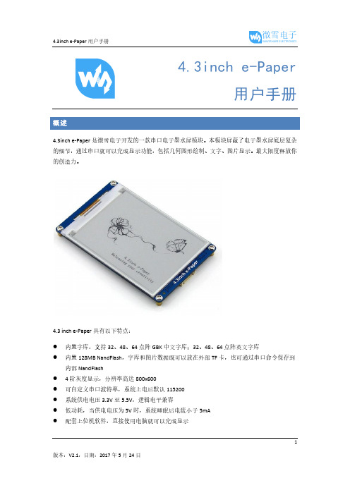
14.3inch e-Paper用户手册4.3inch e-Paper 是微雪电子开发的一款串口电子墨水屏模块。
本模块屏蔽了电子墨水屏底层复杂的细节,通过串口就可以完成显示功能,包括几何图形绘制、文字、图片显示。
最大限度释放你的创造力。
4.3 inch e-Paper 具有以下特点: ● 内置字库,支持32、48、64点阵GBK 中文字库;32、48、64点阵英文字库● 内置128MB NandFlash ,字库和图片数据既可以放在外部TF 卡,也可通过串口命令保存到内部NandFlash● 4阶灰度显示,分辨率高达800x600● 可自定义串口波特率,系统上电后默认115200 ● 系统供电电压3.3V 至5.5V ,逻辑电平兼容● 低功耗,当供电电压为5V 时,系统睡眠后电流小于5mA ●配套上位机软件,直接使用电脑就可以完成显示概述 (1)目录 (2)1.重要提示 (4)2.如何使用 (5)2.1.位图文件的生成 (5)2.2.上位机的使用 (5)2.2.1.硬件连接 (5)2.2.2.安装上位机软件 (5)2.2.3.字库和图片的导入 (7)2.2.4.显示测试 (9)2.3.Arduino (11)2.3.1.硬件连接 (11)2.3.2.程序编译下载 (11)2.4.XNUCLEO-F103RB (11)2.4.1.硬件连接 (11)2.4.2.程序编译下载 (11)2.5.Open103Z (12)2.5.1.硬件连接 (12)2.5.2.程序编译下载 (12)3.串口通信协议 (13)3.1.基本约定 (13)3.1.1.串口说明 (13)23.1.2.指令帧格式 (13)3.1.3.传输顺序 (13)3.1.4.指令参数约定 (13)3.1.5.颜色定义 (13)3.2.指令集 (14)3.2.1.指令速查表 (14)3.2.2.指令详解 (16)4.附录 (21)31.●系统上电系统上电后,会执行一次刷屏操作,将屏幕刷新为白色;如果没有外部TF卡,状态指示灯会闪烁3次并进入常亮;如果有外部TF卡,状态指示灯直接进入常亮。
21.5寸电子班牌规格书-触屏版

语言
OSD
简中/英语
附件
电源线
×1
壁挂支架
×1
合格证
×1
说明书
×1
保修卡
×1
第二章
2.
触摸参数
触摸类型
投射式电容屏
触摸点数
10点
触控压力
<10g
透光率
>92%
连接方式
FPC
响应速度
≤10ms
最小识别点大小
5mm×5mm
最小触点移动检测
1mm
抗光性
具有抗光性
寿命
60000小时
R/L 178 (Min.), U/D 178 (Min.)
寿命
50,000 hrs(min.)
可视面积
476.6mm×268.1mm
帧频率
60Hz
电压供应
5V
安卓配置
CPU
RK3288四核1.8GHzCortex-A17
内部缓存容量(RAM)
2GB
内部存储容量(ROM)
8GB
系统版本
Android5.1
RTC实时时钟
支持 Support
系统升级
支持本地SD,USB升级
外设
摄像头
内置200万高清摄像头支持人脸识别
ARM CortexA7
拾音器
内置高音质麦克风
读卡器
内置IC/ID双频读卡器
电源
电压
100V~240V,50-60Hz
额定功耗
≤35W
待机功率
≤1W
环境
工作温度
0℃~50℃
储藏温度
-20℃~60℃
输入接口
电子电器产品规格书样式

文档* * 电器制造有限公司产品规格书型号:*****芳香器2007 年 4 月28 日制定[变更履历]本规格书适用于****电器制造有限公司针对出口销售于日本国内100V制造的专用产品芳香器。
2.仕样标准仕样3.外观1)颜色各部件颜色符合表面处理表及限度样板。
2)丝印①不能有批伤、印空、脱落等现象。
②印刷色要符合限度样板。
3)标识①标识内容要明确。
符合图纸。
②在指定位置印刷及贴付。
4)制品批号、个・外装箱批号指定位置要正确、明确地标示出。
5)不能有伤、汚、破裂等。
6)电源线有效长度2.5m±2%4.构造,部品1)组装各部品的组装不能强行压入、接合处、间隙等要根据图面要求。
2)部品各部的部品根据图面或部品承认图。
3)空间距离、沿面距离导电体与其它导电体之间的距离 2.5mm以上导电体非导电体之间的距离 2.0mm以上4)内部配线不能触及可动部、高温部、配线装入时不要过分用力。
5)电装部品①、风扇/马达DFB802024L DC 无刷马达24V 1.9W②、恒温器SS1-L AC 125V 2A 78℃±4℃ (OFF)③、云母发热器100V 20W④、门开关SS-01GL-E欧姆龙微型开关DC 30V 0.1A⑤、齿轮马达开关SS-01-E欧姆龙微型开关DC 30V 0.1A⑥、齿轮马达MT8-4 AC100V 50/60Hz 3/2.5W 2.5/3rpm⑦、热敏电阻150-503-7616 R(25℃)=50KΩ B(25℃/50℃)3,590KΩ(3950 KΩ)⑥、电源线线:PVC线VFF 2×0.75㎟(0.18/30芯)灰色3.1M(有效长)±30mm, JET 2220-12009-1001插头:PP成形插头 JET 0883-43001-1001⑦、主基板环氧树脂CEM-1 电流保险丝AC 125V 1A装倾倒开关⑧、操作基板・遥控基板环氧树脂CEM-1 红外线频率38kHz6)包装符合包装仕样书要求。
- 1、下载文档前请自行甄别文档内容的完整性,平台不提供额外的编辑、内容补充、找答案等附加服务。
- 2、"仅部分预览"的文档,不可在线预览部分如存在完整性等问题,可反馈申请退款(可完整预览的文档不适用该条件!)。
- 3、如文档侵犯您的权益,请联系客服反馈,我们会尽快为您处理(人工客服工作时间:9:00-18:30)。
File Name Specification For HINK 1.5'' EPD Module Number HINK-E0154A09 Version A/0Page Number 1 of 32Specification For HINK 1.5''EPDModel NO.:HINK-E0154A09Product VER:V1.1Customer ApprovalCustomerApproval ByDate Of ApprovalPrepared By Checked By Approval ByHu ting Xiao zhongping Cheng weiHu ziping Jia pengfeiFile Name Specification For HINK 1.5'' EPD Module Number HINK-E0154A09 Version A/0Page Number 2 of 32Version Content Date Producer A/0New release2017/06/26Hu tingFile Name Specification For HINK 1.5'' EPD Module Number HINK-E0154A09 Version A/0Page Number 3 of 32CONTENTS1 General Description ... .......................................................................................................... .42 Features ... ........................................................................................................................... . (4)3 Application ... ......................................................................................................................... ..44 Mechanical Specification ...................................................................................................... ..45 Mechanical Drawing of EPD Module ... ............................................................................. ..56 Input/Output Terminals ... ...................................................................................................... ..67 MCU Interface....................................................................................................................... ..7 7.1 MCU Interface Selection ... ............................................................................................ ..77.2 MCU Serial Peripheral Interface (4-wire SPI) ............................................................. ..77.3 MCU Serial Peripheral Interface (3-wire SPI) .............................................................. ..98 Temperature sensor operation... ............................................................................................. .119 COMMAND TABLE... .......................................................................................................... .1210 Reference Circuit... .............................................................................................................. .1611 Absolute Maximum Rating ... ............................................................................................. .1812 DC Characteristics... ............................................................................................................. .1813 Serial Peripheral Interface Timing... .................................................................................... .1914 Power Consumption... .......................................................................................................... .2015 Typical Operating Sequence................................................................................................ ..2015.1 Normal Operation Flow ... ......................................................................................... ..2015.2 Reference program code ... ....................................................................................... . (21)16 Optical Characteristics... ...................................................................................................... ..2216.1 Specifications ... .......................................................................................................... ..22 16.2 Definition Of Contrast Ratio ... .................................................................................. ..2316.3 Reflection Ratio... ....................................................................................................... ..2317 Handing Safety And Environment Requirements... .......................................................... ..2418 Reliability Test...................................................................................................................... ..2619 Block Diagram... .................................................................................................................. ..27 20PartA/PartB specification .................................................................................................... ..2721 Point And Line Standard... .................................................................................................. ..2822 Barcode. ................................................................................................................................. ..3023 Packing.. ................................................................................................................................ ..31File Name Specification For HINK 1.5'' EPD Module Number HINK-E0154A09 Version A/0Page Number 4 of 321. General DescriptionHINK-E0154A09 is an Active Matrix Electrophoretic Display (AMEPD), with interface and a reference system design. The 1.5” active area contains 152×152 pixels, and has 1-bit B/W full display capabilities. An integrated circuit contains gate buffer, source buffer, interface, timing control logic, oscillator, DC-DC. SRAM.LUT, VCOM and border are supplied with each panel.2. Features●152×152 pixels display●White reflectance above 35%●C ontrast ratio above 10:1●U ltra wide viewing angle●U ltra low power consumption●P ure reflective mode●B i-stable display●C ommercial temperature range●L andscape, portrait modes●H ard-coat antiglare display surface●U ltra Low current deep sleep mode●O n chip display RAM●W aveform stored in On-chip OTP●S erial peripheral interface available●O n-chip oscillator●O n-chip booster and regulator control for generating VCOM, Gate and Source driving voltage●I2C signal master interface to read external temperature sensor/built-in temperature sensor3. ApplicationElectronic Shelf Label System4. Mechanical SpecificationsParameter Specifications Unit RemarkScreen Size 1.5InchDisplay Resolution152(H)×152(V) Pixel Dpi:142Active Area27.00 (H)×27.00 (V) mmPixel Pitch0.177×0.177 mmPixel Configuration SquareOutline Dimension37.32(H)×31.80(V) ×1.05(D) mmWeight 2.1±0.2 gFile Name Specification For HINK 1.5'' EPD Module Number HINK-E0154A09 Version A/0Page Number 5 of 325. Mechanical Drawing of EPD moduleFile Name Specification For HINK 1.5'' EPD Module Number HINK-E0154A09 Version A/0Page Number 6 of 32 6. Input/Output TerminalsPin # Single Description Remark1 NC No connection and do not connect with other NC pins Keep Open2 GDR N-Channel MOSFET Gate Drive Control3 RESE Current Sense Input for the Control Loop4 NC No connection and do not connect with other NC pins e Keep Open5 VSH2 Positive Source driving voltage6 TSCL I2C Interface to digital temperature sensor Clock pin7 TSDA I2C Interface to digital temperature sensor Date pin8 BS1 Bus selection pin Note 6-59 BUSY Busy state output pin Note 6-410 RES # Reset Note 6-311 D/C # Data /Command control pin Note 6-212 CS # Chip Select input pin Note 6-113 SCL serial clock pin (SPI)14 SDA serial data pin (SPI)15 VDDIO Power for interface logic pins16 VCI Power Supply pin for the chip17 VSS Ground18 VDD Core logic power pin19 VPP Power Supply for OTP Programming20 VSH1 Power Supply pin for Positive Gate driving voltage andVSH21 VGH Positive Gate driving voltage22 VSL Negative Source driving voltage23 VGL Power Supply pin for Negative Gate driving voltage,VCOM and VSL24 VCOM VCOM driving voltageFile Name Specification For HINK 1.5'' EPD Module Number HINK-E0154A09 Version A/0Page Number7 of 32Note 6-1: This pin (CS#) is the chip select input connecting to the MCU. The chip is enabled for MCU communication:only when CS# is pulled LOW.Note 6-2: This pin (D/C#) is Data/Command control pin connecting to the MCU. When the pin is pulled HIGH,the data will be interpreted as data. When the pin is pulled LOW, the data will be interpreted as command.Note 6-3: This pin (RES#) is reset signal input. The Reset is active low.Note 6-4: This pin (BUSY) is Busy state output pin. When Busy is High the operation of chip should not beinterrupted and any commands should not be issued to the module. The driver IC will put Busy pin High when thedriver IC is working such as:- Outputting display waveform; or- Communicating with digital temperature sensorNote 6-5: This pin (BS1) is for 3-line SPI or 4-line SPI selection. When it is “Low”, 4-line SPI is selected. When it is “High”, 3-line SPI (9 bits SPI) is selected.7.MCU Interface7.1 MCU interface selectionThe HINK-E0154A09 can support 3-wire/4-wire serial peripheral interface. In the Module, the MCU interface is pin selectable by BS1 pins shown in.T able 7-1: MCU interface selectionBS1 MPU InterfaceL4-lines serial peripheral interface (SPI)H3-lines serial peripheral interface (SPI) - 9 bits SPI7.2 MCU Serial Peripheral Interface (4-wire SPI)The 4-wire SPI consists of serial clock SCL, serial data SDA, D/C# and CS#,The control pins status in 4-wire SPI in writing command/data is shown in Table 7- 2and the write procedure 4-wire SPI is shown in Figue 7-2 Table 7-2 : Control pins status of 4-wire SPIFunction SCL pin SDA pin D/C# pin CS# pinWrite command ↑ Command bit L LWrite data ↑ Data bit H LNote:(1)L is connected to V SS and H is connected to V DDIO(2)↑ stands for rising edge of signalFile Name Specification For HINK 1.5'' EPD Module Number HINK-E0154A09 Version A/0Page Number8 of 32In the write mode, SDA is shifted into an 8-bit shift register on each rising edge of SCL in the order of D7, D6, ...D0. The level of D/C# should be kept over the whole byte. The data byte in the shift register is written to the Graphic Display Data RAM (RAM)/Data Byte register or command Byte register according to D/C# pin.Figure 7-2: Write procedure in 4-wire SPI modeIn the Read mode:1.After driving CS# to low, MCU need to define the register to be read.2.SDA is shifted into an 8-bit shift register on each rising edge of SCL in the order of D7, D6, ... D0 with D/C#keep low.3.After SCL change to low for the last bit of register, D/C# need to drive to high.4.SDA is shifted out an 8-bit data on each falling edge of SCL in the order of D7, D6, 05.Depending on register type, more than 1 byte can be read out. After all byte are read, CS# need to drive to highto stop the read operation.Figure 7-2: Read procedure in 4-wire SPI modeFile Name Specification For HINK 1.5''EPD Module NumberHINK-E0154A09VersionA/0Page Number 9 of 327.3 MCU Serial Peripheral Interface (3-wire SPI)The 3-wire SPI consists of serial clock SCL, serial data SDA and CS#. The operation is similar to 4-wire SPI while D/C# pin is not used and it must be tied to LOW. The control pins status in 3-wire SPI is shown in Table 7-3.Table 7-3 : Control pins status of 3-wire SPI FunctionSCL pin SDA pin D/C# pin CS# pin Write command ↑ Command bit Tie LOW L Write data↑Data bitTie LOWLNote:(1)L is connected to V SS and H is connected to V DDIO (2)↑ stands for rising edge of signalIn the write operation, a 9-bit data will be shifted into the shift register on each clock rising edge. The bit shifting sequence is D/C# bit, D7 bit, D6 bit to D0 bit. The first bit is D/C# bit which determines the following byte is command or data. When D/C# bit is 0, the following byte is command. When D/C# bit is 1, the following byte is data. shows the write procedure in 3-wire SPISCLSDA (Write Mode)D7D6D5D4D3D2D1D0CS#D701Figure 7-3: Write procedure in 3-wire SPI modeFile Name Specification For HINK 1.5'' EPD Module Number HINK-E0154A09 Version A/0Page Number10 of 32In the Read mode:1.After driving CS# to low, MCU need to define the register to be read.2.D/C#=0 is shifted thru SDA with one rising edge of SCL3.SDA is shifted into an 8-bit shift register on each rising edge of SCL in the order of D7, D6, 04.D/C#=1 is shifted thru SDA with one rising edge of SCL5.SDA is shifted out an 8-bit data on each falling edge of SCL in the order of D7, D6, 06.Depending on register type, more than 1 byte can be read out. After all byte are read, CS# need to drive to highto stop the read operation.Figure 7-3: Read procedure in 3-wire SPI modeFile Name Specification For HINK 1.5'' EPD Module Number HINK-E0154A09 Version A/0Page Number11 of 328. Temperature sensor operationFollowing is the way of how to sense the ambient temperature of the module. First, use an external temperature sensor to get the temperature value and converted it into HEX format with below mapping table, then send command 0x1A with the HEX temperature value to the module thru the SPI interface.The temperature value to HEX conversion is as follow:1. If the Temperature value MSByte bit D11 = 0, thenThe temperature is positive and value (DegC) = + (Temperature value) / 162. If the Temperature value MSByte bit D11 = 1, thenThe temperature is negative and value (DegC) = ~ (2’s complement of Temperature value) / 16File Name Specification For HINK 1.5'' EPD Module Number HINK-E0154A09 Version A/0Page Number12 of 329. COMMAND TABLER/W# D/C# Hex D7 D6 D5 D4 D3 D2 D1 D0 Command Description0 0 01 0 0 0 0 0 0 0 1 Driver OutputControl Set the number of gate. Setting for 152 gates is: Set A[8:0] = 97hSet B[7:0] = 00h0 1 - A7A6A5A4A3A2A1A0 0 1 - 0 0 0 0 0 0 0 A8 0 1 - 0 0 0 0 0 B2B1B00 0 03 0 0 0 0 0 0 1 1 Gate DrivingV oltageControl Set Gate driving voltage.A[4:0] = 19h [POR], VGH at 21V0 1 - 0 0 0 A4A3A2A1A00 0 04 0 0 0 0 0 1 0 0 SourceDrivingvoltageControl Set Source output voltage.A[7:0] = 41h [POR], VSH1 at 15V B[7:0] = A8h [POR], VSH2 at 5V C[7:0] = 32h [POR], VSL at -15V0 1 - A7B7C7 A6B6C6A5B5C5A4B4C4A3B3C3A2B2C2A1B1C1A0B0C00 0 10 0 0 0 1 0 0 0 0 Deep SleepMode Deep Sleep mode ControlA[1:0] Description00 Normal Mode [POR]01 Enter Deep Sleep Mode1 11 Enter Deep Sleep Mode20 1 - 0 0 0 0 0 0 A1 A00 0 11 0 0 0 1 0 0 0 1 Data Entrymodesetting Define data entry sequence.A[2:0] = 3h [POR],A [1:0] = ID[1:0]Address automatic increment / decrementsettingThe setting of incrementing or decrementing of the address counter can be made independently in each upper and lower bit of the address.00 –Y decrement, X decrement,01 –Y decrement, X increment,10 –Y increment, X decrement,11 –Y increment, X increment [POR]A[2] = AMSet the direction in which the address counter is updated automatically after data is written to the RAM.When AM= 0, the address counter is updated in the X direction. [POR]When AM = 1, the address counter is updated in the Y direction.0 1 - 0 0 0 0 0 A2A1A00 0 12 0 0 0 1 0 0 1 0 SW RESET It resets the commands and parameters totheir S/W Reset default values exceptR10h-Deep Sleep ModeDuring operation, BUSY pad will output high.Note: RAM are unaffected by this command.0 0 14 0 0 0 1 0 1 0 0 HV ReadyDetectionHV ready detectionThe command required CLKEN=1 andANALOGEN=1Refer to Register 0x22 for detail.After this command initiated, HV Ready detectionstarts.BUSY pad will output high during detection.The detection result can be read from the Status BitRead (Command 0x2F).File Name Specification For HINK 1.5'' EPD Module Number HINK-E0154A09 Version A/0Page Number13 of 32R/W# D/C# Hex D7 D6 D5 D4 D3 D2 D1 D0 Command Description0 0 15 0 0 0 1 0 1 0 1 VCIDetection A[2:0] = 100 [POR] , Detect level at 2.3VA[2:0] : VCI level DetectA[2:0] VCI level011 2.2V100 2.3V101 2.4V110 2.5V111 2.6VOther NAThe command required CLKEN=1 and ANALOGEN=1Refer to Register 0x22 for detail.After this command initiated, VCI detection starts. BUSY pad will output high during detection.The detection result can be read from the Status Bit Read (Command 0x2F).0 1 0 0 0 0 0 A2A1A00 0 1A 0 0 0 1 1 0 1 0 TemperatureSensorControl(Write totemperatureregister) Write to temperature register. A[11:0] =7FFH[POR]0 1 - A11A10A9A8A7A6A5A40 1 - A3A2A1A00 0 0 00 0 20 0 0 1 0 0 0 0 0 MasterActivationActivate Display Update Sequence.The Display Update Sequence Option islocated at R22hBUSY pad will output high during operation.User should not interrupt this operation to avoidcorruption of panel images.0 0 21 0 0 1 0 0 0 0 1 DisplayUpdateControl 1 RAM content option for Display Update A[7:0] = 00h [POR]A[7:4] Red RAM option0000 Normal0100 Bypass RAM content as 0 1000 Inverse RAM contentA[3:0] BW RAM option0000 Normal0100 Bypass RAM content as 0 1000 Inverse RAM content0 1 - A7A6A5A4A3A2A1A00 0 22 0 0 1 0 0 0 1 0 DisplayUpdateControl 2 Display Update Sequence Option:Enable the stage for Master ActivationA[7:0]=FFh (POR)Parameter(in Hex) Enable Clock Signal,Then Enable AnalogThen DISPLAYThen Disable AnalogThen Disable OSCC7Load LUT from OTPEnable Clock Signal,Then Load LUTThen Disable OSC910 1 - A7A6A5A4A3A2A1A00 0 24 0 0 1 0 0 1 0 0 WriteRAM(BW) After this command, data entries will be written into the RAM until another command is written. Address pointers will advance accordingly.For Write pixel:Content of Write RAM(BW)=1For Black pixel:Content of Write RAM( BW)=00 0 26 0 0 1 0 0 1 1 0 WriteRAM(RED) After this command, data entries will be written into the RED RAM until another command is written. Address pointers will advance accordingly. For Red pixel:Content of Write RAM(RED)=1For non-Red pixel[Black or White]:Content of Write RAM(RED)=0File Name Specification For HINK 1.5'' EPD Module Number HINK-E0154A09 Version A/0Page Number14 of 32R/W# D/C# Hex D7 D6 D5 D4 D3 D2 D1 D0 Command Description0 0 2C 0 0 1 0 1 1 0 0 Write VCOMregister Write VCOM register from MCU interfaceA[7:0]=00h[POR]A[7:0] VCOM (V) A[7:0] VCOM (V) 08h -0.2 44h -1.70Bh -0.3 48h -1.810h -0.4 4Bh -1.914h -0.5 50h -217h -0.6 54h -2.11Bh -0.7 58h -2.220h -0.8 5Bh -2.324h -0.9 5Fh -2.428h -1 64h -2.52Ch -1.1 68h -2.62Fh -1.2 6Ch -2.734h -1.3 6Fh -2.837h -1.4 73h -2.93Ch -1.5 78h -340h -1.6 Other NA0 1 - A7A6A5A4A3A2A1A00 0 2D 0 0 1 0 1 1 0 1 OTP RegisterRead Read Register stored in OTP:1. A[7:0]~ B[7:0]: VCOM Information3. C[7:0]~F[7:0]: Reserved4. G[7:0]~H[7:0]: Module ID/ Waveform Version [2bytes]0 1 A7A6A5A4A3A2A1A0…0 1 H7H6H5H4H3H2H1H00 0 2F 0 0 1 0 1 0 0 1 Status Bit Read Read IC status Bit [POR 0x21]A[5]: HV Ready Detection flag [POR=1]0: Ready1: Not ReadyA[4]: VCI Detection flag [POR=0]0: Normal1: VCI lower than the Detect levelA[3]: [POR=0]A[2]: Busy flag [POR=0]0: Normal1: BUSYA[1:0]: Chip ID [POR=01]Remark:A[5] and A[4] status are not valid after RESET, theyneed to be initiated by command 0x14 and command0x15 respectively.1 1 - 0 0 0 A40 0 A1A00 0 32 0 0 1 1 0 0 1 0 Write LUTregister Write LUT register from MCU interface [70 bytes] (excluding the analog setting and frame setting)0 1 - A7A6A5A4A3A2A1A0 0 1 - B7B6B5B4B3B2B1B0 0 1 - : : : : : : : : 0 1 - . . . . . . . .0 0 3A 0 0 1 1 1 0 1 0 Set dummy lineperiod Set A[7:0] = 0Fh0 1 - 0 A6A5A4A3A2A1A00 0 3B 0 0 1 1 1 0 1 1 Set Gate linewidth Set A[3:0] = 0Ch0 1 - 0 0 0 0 A3A2A1A0File Name Specification For HINK 1.5'' EPD Module Number HINK-E0154A09 Version A/0Page Number15 of 32R/W# D/C# Hex D7 D6 D5 D4 D3 D2 D1 D0 Command Description0 0 3C 0 0 1 1 1 1 0 0 BorderWaveformControl Select border waveform for VBDA [7:6] Select VBDA[7:6] Select VBD as00[POR] GS Transition DefineA[1:0]01 Fix Level Define A[5:4]10 VCOM11 HIZA [5:4] Fix Level Setting for VBDA[5:4] VBD level00[POR] VSS01 VSH110 VSL11 VSH2A[1:0]) GS Transition setting for VBDA[1:0] VBD Transition00 [POR] LUT001 LUT110 LUT211 LUT30 1 - A7A6A5A40 0 A1A00 0 44 0 1 0 0 0 1 0 0 Set RAM X -addressStart / Endposition Specify the start/end positions of the window address in the X direction by an address unitA[4:0]: X-Start, POR = 00hB[4:0]: X-End, POR = 12h0 1 - 0 0 0 A4A3A2A1A0 0 1 - 0 0 0 B4B3B2B1B00 0 45 0 1 0 0 0 1 0 1 Set Ram Y-addressStart / Endposition Specify the start/end positions of the window address in the Y direction by an address unitA[7:0]: Y-Start, POR = 00hB[7:0]: Y-End, POR = F9h0 1 - A7A6A5A4A3A2A1A0 0 1 0 0 0 0 0 0 0 A8 0 1 - B7B6B5B4B3B2B1B0 0 1 0 0 0 0 0 0 0 B80 0 4E 0 1 0 0 1 1 1 0 Set RAM X -addresscounter Make initial settings for the RAM X address in the address counter (AC) A[4:0] : POR is 00h0 1 - 0 0 0 A4A3A2A1A00 0 4F 0 1 0 0 1 1 1 1 Set RAM Y -addresscounter Make initial settings for the RAM Y address in the address counter (AC) A[7:0] : POR is 00h0 1 - A7A6A5A4A3A2A1A00 0 0 0 0 0 0 A80 0 74 0 1 1 1 0 1 0 0 Set AnalogBlockcontrol A[7:0] = 54h0 1 A7A6A5A4A3A2A1A00 0 7E 0 1 1 1 1 1 1 0 Set DigitalBlockcontrol A[7:0] = 3Bh0 1 A7A6A5A4A3A2A1A0File Name Specification For HINK 1.5'' EPD Module Number HINK-E0154A09 Version A/0Page Number16 of 3210.Reference CircuitFigure. 10-1File Name Specification For HINK 1.5'' EPD Module Number HINK-E0154A09 Version A/0Page Number17 of 32Figure. 10-2File Name Specification For HINK 1.5'' EPD Module Number HINK-E0154A09 Version A/0Page Number18 of 3211. ABSOLUTE MAXIMUM RATINGT able 11-1: Maximum RatingsSymbol Parameter Rating UnitV CI Logic supply voltage -0.5 to +6.0 VT OPR Operation temperature range 0 to 50 °CT STG Storage temperature range -25 to 60 °C12.DC CHARACTERISTICSThe following specifications apply for: VSS=0V, VCI=3.3V, T OPR=25℃.Table 12-1: DC CharacteristicsSymbol Parameter T est Condition Applicable pin Min. Typ. Max. Unit VCI VCI operation voltage - VCI 2.2 3.3 3.7 VVIH High level input voltage - SDA, SCL, CS#,D/C#, RES#, 0.8VDDIO- - VVIL Low level input voltage - - - 0.2VDDIOVVOH High level output voltage IOH = -100uA BUSY 0.9VDDIO- - VVOL Low level output voltage IOL = 100uA - - 0.1VDDIOV Iupdate Module operating current- - - 3 - mA Isleep Deep sleep mode VCI=3.3V- - 0.6 1 uA - The Typical power consumption is measured using associated 25℃ waveform with followingpattern transition: from horizontal scan pattern to vertical scan pattern. (Note 12-1)- The listed electrical/optical characteristics are only guaranteed under the controller &waveform provided by XingTai.- Vcom value will be OTP before in factory or present on the label sticker.N ote 12-1The Typical power consumptionFile Name Specification For HINK 1.5'' EPD Module Number HINK-E0154A09 Version A/0Page Number19 of 3213. Serial Peripheral Interface TimingThe following specifications apply for: VSS=0V, VCI=2.2V to 3.7V, T OPR=25℃Write modeSymbol Parameter Min Typ Max Unit fSCL SCL frequency (Write Mode) 20 MHz tCSSU Time CS# has to be low before the first rising edge of SCLK 20 ns tCSHLD Time CS# has to remain low after the last falling edge of SCLK 20 ns tCSHIGH Time CS# has to remain high between two transfers 100 ns tSCLHIGH Part of the clock period where SCL has to remain high 25 ns tSCLLOW Part of the clock period where SCL has to remain low 25 ns tSISU Time SI (SDA Write Mode) has to be stable before the next rising edge of SCL 10 ns tSIHLD Time SI (SDA Write Mode) has to remain stable after the rising edge of SCL 40 ns Read modeSymbol Parameter Min Typ Max Unit fSCL SCL frequency (Read Mode) 2.5 MHz tCSSU Time CS# has to be low before the first rising edge of SCLK 100 ns tCSHLD Time CS# has to remain low after the last falling edge of SCLK 50 ns tCSHIGH Time CS# has to remain high between two transfers 250 ns tSCLHIGH Part of the clock period where SCL has to remain high 180 ns tSCLLOW Part of the clock period where SCL has to remain low 180 ns tSOSU Time SO(SDA Read Mode) will be stable before the next rising edge of SCL 50 ns tSOHLD Time SO (SDA Read Mode) will remain stable after the falling edge of SCL 0 ns Note: All timings are based on 20% to 80% of VDDIO-VSSFigure 13-1 : Serial peripheral interface characteristics14 .Power ConsumptionParameter Symbol Conditions TYP Max Unit Remark Panel power consumption during update - 25℃ 5.8 - mAs - Deep sleep mode - 25℃0.6 - uA -File Name Specification For HINK 1.5'' EPD Module Number HINK-E0154A09Version A/0Page Number20 of 3215. Typical Operating Sequence 15.1 Normal Operation FlowFile Name Specification For HINK 1.5'' EPD Module Number HINK-E0154A09 Version A/0Page Number21 of 3215.2 Reference Program CodeFile Name Specification For HINK 1.5'' EPD Module Number HINK-E0154A09 Version A/0Page Number22 of 3216. Optical characteristics16.1 SpecificationsMeasurements are made with that the illumination is under an angle of 45 degrees, the detection is perpendicular unless otherwise specified.T=25℃SYMBOL PARAMETER CONDITIONSMIN TYPE MAX UNIT NoteR Reflectance White 30 35 - % Note 16-1 Gn 2Grey Level - - DS+(WS-DS)×n(m-1) - L* - CR Contrast Ratio indoor - 10 - - - Panel’s life- 0℃~50℃5years or 1000000 times - - Note 16-2WS: White state, DS : Dark statem: 2Note 16-1: Luminance meter : Eye - One Pro SpectrophotometerNote 16-2: We guarantee display quality from 0℃~30℃ generally,If operation ambient temperature from 30~50℃,will Offer special waveform by Xingtai.File Name Specification For HINK 1.5'' EPD Module Number HINK-E0154A09 Version A/0Page Number23 of 3216.2 Definition of contrast ratioThe contrast ratio (CR) is the ratio between the reflectance in a full white area (R1) and the reflectance in a dark area (Rd)() :R1: white reflectance Rd: dark reflectanceCR = R1/Rd16.3 Reflection RatioThe reflection ratio is expressed as :R = Reflectance Factor white board x (L center / L white board )L center is the luminance measured at center in a white area (R=G =B=1) . L white board is the luminance of a standard white board . Both are measured with equivalent illumination source . The viewing angle shall be no more than 2 degrees .File Name Specification For HINK 1.5'' EPD Module Number HINK-E0154A09 Version A/0Page Number24 of 3217. HANDLING,SAFETY AND ENVIROMENTAL REQUIREMENTSW ARNINGThe display glass may break when it is dropped or bumped on a hard surface. Handle with care. Should the display break, do not touch the electrophoretic material. In case of contact with electrophoretic material, wash with water and soap.CAUTIONThe display module should not be exposed to harmful gases, such as acid and alkali gases, which corrode electronic components.Disassembling the display module can cause permanent damage and invalidate the warranty agreements.IPA solvent can only be applied on active area and the back of a glass. For the rest part, it is not allowed.Observe general precautions that are common to handling delicate electronic components. The glass can break andfront surfaces can easily be damaged . Moreover the display is sensitive to static electricity and other roughenvironmental conditions.Mounting Precautions(1) It`s recommended that you consider the mounting structure so that uneven force (ex. Twisted stress) is not applied tothe module.(2) It`s recommended that you attach a transparent protective plate to the surface in order to protect the EPD.Transparent protective plate should have sufficient strength in order to resist external force.(3) You should adopt radiation structure to satisfy the temperature specification.(4) Acetic acid type and chlorine type materials for the cover case are not desirable because the former generatescorrosive gas of attacking the PS at high temperature and the latter causes circuit break by electro-chemical reaction.(5) Do not touch, push or rub the exposed PS with glass, tweezers or anything harder than HB pencil lead. And please donot rub with dust clothes with chemical treatment. Do not touch the surface of PS for bare hand or greasy cloth. (Some cosmetics deteriorate the PS)(6) When the surface becomes dusty, please wipe gently with absorbent cotton or other soft materials like chamois soakswith petroleum benzene. Normal-hexane is recommended for cleaning the adhesives used to attach the PS. Do not use acetone, toluene and alcohol because they cause chemical damage to the PS.(7) Wipe off saliva or water drops as soon as possible. Their long time contact with PS causes deformations and colorfading.Product specification The data sheet contains final product specifications.。