自上而下(Top-down)方法实现高密度垂直硅纳米线(Vertical Si NWs)阵列
半导体硅片生产标准工艺标准流程及标准工艺注意要点
硅片生产工艺流程及注意要点简介硅片旳准备过程从硅单晶棒开始,到清洁旳抛光片结束,以可以在绝好旳环境中使用。
期间,从一单晶硅棒到加工成数片能满足特殊规定旳硅片要经过诸多流程和清洗环节。
除了有许多工艺环节之外,整个过程几乎都要在无尘旳环境中进行。
硅片旳加工从一相对较脏旳环境开始,最后在10级净空房内完毕。
工艺过程综述硅片加工过程涉及许多环节。
所有旳环节概括为三个重要种类:能修正物理性能如尺寸、形状、平整度、或某些体材料旳性能;能减少不期望旳表面损伤旳数量;或能消除表面沾污和颗粒。
硅片加工旳重要旳环节如表1.1旳典型流程所示。
工艺环节旳顺序是很重要旳,由于这些环节旳决定能使硅片受到尽量少旳损伤并且可以减少硅片旳沾污。
在如下旳章节中,每一环节都会得到具体简介。
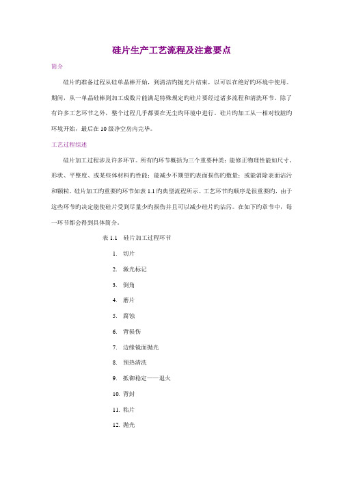
表1.1 硅片加工过程环节1.切片2.激光标记3.倒角4.磨片5.腐蚀6.背损伤7.边缘镜面抛光8.预热清洗9.抵御稳定——退火10.背封11.粘片12.抛光13.检查前清洗14.外观检查15.金属清洗16.擦片17.激光检查18.包装/货运切片(class 500k)硅片加工旳简介中,从单晶硅棒开始旳第一种环节就是切片。
这一环节旳核心是如何在将单晶硅棒加工成硅片时尽量地降低损耗,也就是规定将单晶棒尽量多地加工成有用旳硅片。
为了尽量得到最佳旳硅片,硅片规定有最小量旳翘曲和至少量旳刀缝损耗。
切片过程定义了平整度可以基本上适合器件旳制备。
切片过程中有两种重要方式——内圆切割和线切割。
这两种形式旳切割方式被应用旳因素是它们能将材料损失减少到最小,对硅片旳损伤也最小,并且容许硅片旳翘曲也是最小。
切片是一种相对较脏旳过程,可以描述为一种研磨旳过程,这一过程会产生大量旳颗粒和大量旳很浅表面损伤。
硅片切割完毕后,所粘旳碳板和用来粘碳板旳粘结剂必须从硅片上清除。
在这清除和清洗过程中,很重要旳一点就是保持硅片旳顺序,由于这时它们还没有被标记辨别。
激光标记(Class 500k)在晶棒被切割成一片片硅片之后,硅片会被用激光刻上标记。
纳米银线的制备方法综述
纳米银线的制备方法综述吴永谦;张卜升;陈昆昆;孟晗琪;操齐高【摘要】纳米银线(AgNWs)由于其优良的导电性、导热性、柔韧性及纳米材料独特的尺寸效应有望替代ITO成为新一代的透明导电膜材料而引起广泛的关注.综述介绍了多元醇法、晶种法、水热法、模板法、湿化学法及其他一些化学制备AgNWs的方法,提出由实验室制备向工业化批量生产的发展方向.%Silver nanowires (AgNWs) have attracted considerable attention because of their excellent electrical conductivity, thermal conductivity, flexibility and unique size effects of nanomaterials, are expected to replace ITO as a new generation of transparent conductive film materials. Various synthesis of silver nanowires, such as polyol method, seeded method, hydrothermal method, wet chemical method and template method, were reviewed. The development trend of laboratory preparation to industrial production was put forward.【期刊名称】《贵金属》【年(卷),期】2017(038)0z1【总页数】4页(P108-111)【关键词】纳米银线;制备;多元醇法;晶种法;水热法;湿化学法【作者】吴永谦;张卜升;陈昆昆;孟晗琪;操齐高【作者单位】西北有色金属研究院,西安 710016;西北有色金属研究院,西安710016;西北有色金属研究院,西安 710016;西北有色金属研究院,西安 710016;西北有色金属研究院,西安 710016【正文语种】中文【中图分类】TF832透明导电膜(transparent conducting film,TCF)是一种具有良好透光性和导电性的材料,广泛应用于有机发光二极管(OLED)、太阳能电池、平板显示器、触摸屏、智能玻璃等领域。
半导体工艺复习整理

工艺考试复习:整理者(butterflying 2011‐1‐11)1.在半导体技术发展的过程中有哪些重要事件?(一般)晶体管的诞生集成电路的发明平面工艺的发明CMOS技术的发明2.为什么硅是半导体占主导的材料?有哪些硅基薄膜?(一般)硅材料:优良的半导体特性、稳定的电的、化学的、物理的及机械的性能(特性稳定的金刚石晶体结构、良好的传导特性、优异的工艺加工能力、研究最透彻的材料、具有一系列的硅基化合物)(总结:半导体性、电、物理、化学、机械性)硅基薄膜:外延硅薄膜、多晶硅薄膜、无定形硅薄膜、SiO2与Si3N4介质膜、SiGe薄膜、金属多晶硅膜3. 微电子技术发展基本规律是什么?(重要)摩尔定律(Moore’s Law):芯片内的晶体管数量每18个月~20个月增加1倍――集成电路的集成度每隔三年翻两番,器件尺寸每三年增加0.7 倍,半导体技术和工业呈指数级增长。
特征尺寸缩小因子,250→180→130→90→65→45→32→22→16(nm)等比例缩小比率(Scaling down principle):在MOS器件内部恒定电场的前提下,器件的横向尺寸、纵向尺寸、电源电压都按照相同的比例因子k缩小,从而使得电路集成度k2倍提高,速度k倍提高,功耗k2倍缩小。
MOS管阻抗不变,但连线电阻和线电流密度都呈k倍增长。
(阈值电压不能缩得太小,电源电压要保持长期稳定)(总结:尺寸、电源电压变为1/k,集成度变为k^2.速度变为k倍。
(掺杂浓度变为k倍)Device miniaturization by “ Scaling‐down Principle”− Device geometry‐L g, W g, t ox, x j ⋅ 1/k− Power supply‐V dd ⋅1/k− Substrate doping‐N ⋅ k®Device speed ⋅ k® Chip density ⋅ k24. 什么是ITRS ?(重要)International Technology Roadmap for Semiconductors国际半导体技术发展蓝图技术节点:DRAM半间距Technology node = DRAM half pitch5. 芯片制造的主要材料和技术是什么?(一般)Si材料:大直径和低缺陷的单晶硅生长、吸杂工艺、薄膜的外延生长、SiGe/Si异质结、SOI 介质薄膜材料和工艺:热氧化、超薄高K栅氧化薄膜生长、互连的低K介质;高分辨率光刻:电子束掩膜版、光学光刻(电子束曝光EBL)、匹配光刻。
高分子论文参考文献
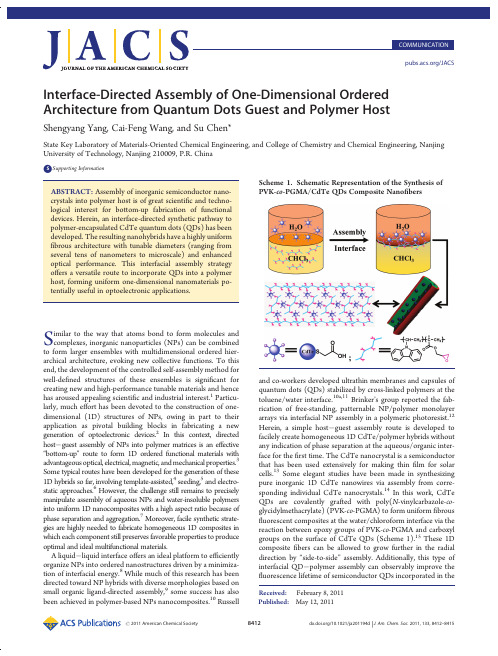
Published:May 12,2011COMMUNICATION /JACSInterface-Directed Assembly of One-Dimensional Ordered Architecture from Quantum Dots Guest and Polymer HostShengyang Yang,Cai-Feng Wang,and Su Chen*State Key Laboratory of Materials-Oriented Chemical Engineering,and College of Chemistry and Chemical Engineering,Nanjing University of Technology,Nanjing 210009,P.R.ChinabSupporting Information ABSTRACT:Assembly of inorganic semiconductor nano-crystals into polymer host is of great scienti fic and techno-logical interest for bottom-up fabrication of functional devices.Herein,an interface-directed synthetic pathway to polymer-encapsulated CdTe quantum dots (QDs)has been developed.The resulting nanohybrids have a highly uniform fibrous architecture with tunable diameters (ranging from several tens of nanometers to microscale)and enhanced optical performance.This interfacial assembly strategy o ffers a versatile route to incorporate QDs into a polymer host,forming uniform one-dimensional nanomaterials po-tentially useful in optoelectronic applications.Similar to the way that atoms bond to form molecules and complexes,inorganic nanoparticles (NPs)can be combined to form larger ensembles with multidimensional ordered hier-archical architecture,evoking new collective functions.To this end,the development of the controlled self-assembly method for well-de fined structures of these ensembles is signi ficant for creating new and high-performance tunable materials and hence has aroused appealing scienti fic and industrial interest.1Particu-larly,much e ffort has been devoted to the construction of one-dimensional (1D)structures of NPs,owing in part to their application as pivotal building blocks in fabricating a new generation of optoelectronic devices.2In this context,directed host Àguest assembly of NPs into polymer matrices is an e ffective “bottom-up ”route to form 1D ordered functional materials with advantageous optical,electrical,magnetic,and mechanical properties.3Some typical routes have been developed for the generation of these 1D hybrids so far,involving template-assisted,4seeding,5and electro-static approaches.6However,the challenge still remains to precisely manipulate assembly of aqueous NPs and water-insoluble polymers into uniform 1D nanocomposites with a high aspect ratio because of phase separation and aggregation.7Moreover,facile synthetic strate-gies are highly needed to fabricate homogeneous 1D composites in which each component still preserves favorable properties to produce optimal and ideal multifunctional materials.A liquid Àliquid interface o ffers an ideal platform to e fficiently organize NPs into ordered nanostructures driven by a minimiza-tion of interfacial energy.8While much of this research has been directed toward NP hybrids with diverse morphologies based on small organic ligand-directed assembly,9some success has also been achieved in polymer-based NPs nanocomposites.10Russelland co-workers developed ultrathin membranes and capsules of quantum dots (QDs)stabilized by cross-linked polymers at the toluene/water interface.10a,11Brinker ’s group reported the fab-rication of free-standing,patternable NP/polymer monolayer arrays via interfacial NP assembly in a polymeric photoresist.12Herein,a simple host Àguest assembly route is developed to facilely create homogeneous 1D CdTe/polymer hybrids without any indication of phase separation at the aqueous/organic inter-face for the first time.The CdTe nanocrystal is a semiconductor that has been used extensively for making thin film for solar cells.13Some elegant studies have been made in synthesizing pure inorganic 1D CdTe nanowires via assembly from corre-sponding individual CdTe nanocrystals.14In this work,CdTe QDs are covalently grafted with poly(N -vinylcarbazole-co -glycidylmethacrylate)(PVK-co -PGMA)to form uniform fibrous fluorescent composites at the water/chloroform interface via the reaction between epoxy groups of PVK-co -PGMA and carboxyl groups on the surface of CdTe QDs (Scheme 1).15These 1D composite fibers can be allowed to grow further in the radial direction by “side-to-side ”assembly.Additionally,this type of interfacial QD Àpolymer assembly can observably improve the fluorescence lifetime of semiconductor QDs incorporated in theScheme 1.Schematic Representation of the Synthesis of PVK-co -PGMA/CdTe QDs Composite Nano fibersReceived:February 8,2011polymeric matrix.It can be expected that this example of both linear axial organization and radial assembly methodology can be applied to fabricate spatial multiscale organic Àinorganic com-posites with desired properties of NPs and polymers.Figure 1a shows a typical scanning electron microscope (SEM)image of PVK-co -PGMA/CdTe QDs composite nano fi-bers obtained at the water/chloroform interface after dialysis.The as-prepared fibers have uniform diameters of about 250nm and typical lengths in the range of several tens to several hundreds of micrometers (Figures 1a and S4Supporting In-formation [SI]).Interestingly,PVK-co -PGMA/CdTe composite fibers can randomly assemble into nestlike ring-shaped patterns (Figures 1b and S5[SI]).Given the interaction among epoxy groups,the formation of nestlike microstructures could be attributed to incidental “head-to-tail ”assembly of composite fibers.Moreover,in order to establish the relationship between the role of epoxy groups and the formation of composite nano fibers,control experiments were performed,in which pure PGMA or PVK was used to couple CdTe QDs.The PGMA/CdTe composites could be obtained with fibrous patterns (Figure S6[SI]),but no fibrous composites were achieved at the biphase interface with the use of PVK under the same conditions.The microstructures and fluorescence properties of PVK-co -PGMA/CdTe composite fibers were further character-ized using laser confocal fluorescence microscopy (LCFM).Confocal fluorescence micrographs of composite fibers show that the di fferently sized QDs have no obvious in fluence on the morphology of composites (Figure 1c Àe).Clearly,uniform and strong fluorescence emission is seen throughout all the samples,and the size-dependent fluorescence trait of CdTe QDs in PVK-co -PGMA matrix remains well.In order to verify the existence and distribution of CdTe QDs in the fibers,transmission electron microscopy (TEM)was employed to examine the assembled structures.Figure 2a shows a TEM image of PVK-co -PGMA/CdTe QDs composite nano fi-bers,indicating each composite fiber shown in Figure 1a was assembled from tens of fine nano fibers.An individual fine nano fiber with the diameter of about 30nm is displayed in Figure 2b,from which we can see that CdTe QDs have been well anchored into the fiber with polymeric protection layer,revealing this graft-form process at the interface e ffectively avoidednon-uniform aggregation in view of well-dispersed CdTe QDs within the composite fiber,consistent with the LCFM observa-tion.Unlike previous works where the nanoparticles were ad-sorbed onto the polymer fibers,16CdTe QDs were expelled from the surface of fibers (∼2.5nm)in our system (Figure 2c),albeit the high percentage of QDs in the polymer host (23wt %)was achieved (Figure S7[SI]).This peculiarity undoubtedly confers CdTe QDs with improved stability.The clear di ffuse rings in the selected area electron di ffraction (SAED)pattern further indicate excellent monodispersion and finely preserved crystalline struc-ture of QDs in the nano fibers (Figure 2d).The SAED data correspond to the cubic zinc blende structure of CdTe QDs.A possible mechanism for the assembly of 1D nanostructure was proposed,as illustrated in Figure S8[SI].The hydrophilic epoxy groups of the PVK-co -PGMA chain in the oil phase orient toward the biphase interface and then react with carboxyl groups on the surface of CdTe QDs in the aqueous phase to a fford premier PVK-co -PGMA/CdTe QDs composites.Such nanocomposites will reverse repeatedly,resulting from iterative reaccumulation of epoxy groups at the interface and the reaction between the active pieces (i.e.,epoxy or carboxyl groups)in the composites with intact CdTe QDs or PVK-co -PGMA,forming well-de fined nano-fibers.The control experiments showing that the diameter of composite fibers increases with the increase in the concentration of PVK-co -PGMA are in agreement with the proposed mechan-ism (Figure S9[SI]).In addition,it is expected that the pure polymeric layer on the surface of the fibers (red rectangular zone in Figure 2c)will allow further assembly of fine fibers into thick fibers,and these fibers also could randomly evolve into rings,forming nestlike microstructures when the “head ”and “tail ”of fibers accidentally meet (Figure 1b).To further examine the assembly behavior of composite fibers,the sample of PVK-co -PGMA/CdTe QDs composite nano fibers were kept at the water/chloroform interface for an additional month in a close spawn bottle at room temperature (Figure S10[SI]).With longer time for assembly,thicker composite fibers with tens of micrometers in diameter were obtained (Figure 3a).These micro-fibers have a propensityto form twisted morphology (Figure 3a,b),Figure 1.(a,b)SEM images of PVK-co -PGMA/CdTe QDs composite nano fibers.(c Àe)Fluorescence confocal microscopy images of PVK-co -PGMA/CdTe QDs composite nano fibers in the presence of di fferently sized QDs:(c)2.5nm,(d)3.3nm,and (e)3.6nm.The excitation wavelengths are 488(c),514(d),and 543nm (e),respectively.Figure 2.(a,b)TEM images of PVK-co -PGMA/CdTe QDs composite nano fibers,revealing composite nano fiber assemblies.(c)HRTEM image and (d)SAED pattern of corresponding PVK-co -PGMA/CdTe QDs composite nano fibers.while their re fined nanostructures still reveal relatively parallel character and con firm the micro fibers are assembled from countless corresponding nano fibers (Figure 3c).The corresponding LCFM image of an individual micro fiber is shown in Figure 3d (λex =488nm),indicating strong and homogeneous green fluorescence.Another indication is the fluorescent performance of PVK-co -PGMA/CdTe QDs composite micro fibers (Figure 4a).The fluorescent spectrum of composite fibers takes on emission of both PVK-co -PGMA and CdTe QDs,which suggests that this interfacial assembly route is e ffective in integrating the properties of organic polymer and inorganic nanoparticles.It is worth noting that there is a blue-shift (from 550to 525nm)and broadening of the emission peak for CdTe QDs upon their incorporation into polymeric hosts,which might be ascribed to the smaller QD size and less homogeneous QD size distribution resulting from the photooxidation of QD surfaces.17Since the emission spectra of PVK-co -PGMA spectrally overlap with the CdTe QD absorption (Figure S11[SI]),energy transfer from the copolymer to the CdTe QDs should exist.18However,the photoluminescence of PVK-co -PGMA does not vanish greatly in the tested sample in comparison with that of polymer alone,revealing inferior energy transfer between the polymer host and the QDs.Although e fficient energy transfer could lead to hybrid materials that bring together the properties of all ingredients,18it is a great hurdle to combine and keep the intrinsic features of all constituents.19In addition,by changing the polymeric compo-nent and tailoring the element and size of QDs,it should be possible to expect the integration of organic and inorganic materials with optimum coupling in this route for optoelectronic applications.Finally,to assess the stability of CdTe QDs in the composite micro fibers,time-resolved photoluminescence was performed using time-correlated single-photon counting (TCSPC)parative TCSPC studies for hybrid PVK-co -PGMA/CdTe QDs fibers and isolated CdTe QDs in the solid state are presented in Figure 4b.We can see that the presence of PVK-co -PGMA remarkably prolongs the fluorescence lifetime (τ)of CdTe QDs.Decay traces for the samples were well fittedwith biexponential function Y (t )based on nonlinear least-squares,using the following expression.20Y ðt Þ¼R 1exp ðÀt =τ1ÞþR 2exp ðÀt =τ2Þð1Þwhere R 1,R 2are fractional contributions of time-resolved decaylifetimes τ1,τ2and the average lifetime τhcould be concluded from the eq 2:τ¼R 1τ21þR 2τ22R 1τ1þR 2τ2ð2ÞFor PVK-co -PGMA/CdTe QDs system,τh is 10.03ns,which is approximately 2.7times that of isolated CdTe QDs (3.73ns).Photooxidation of CdTe QDs during the assembly process can increase the surface states of QDs,causing a delayed emission upon the carrier recombination.21Also,the polymer host in this system could prevent the aggregation of QDs,avoid self-quench-ing,and delay the fluorescence decay process.22The increased fluorescence lifetime could be also ascribed to energy transfer from PVK-co -PGMA to CdTe QDs.18c The result suggests that this host Àguest assembly at the interface could find signi ficant use in the fabrication of QDs/polymer hybrid optoelectronic devices.In summary,we have described the first example of liquid/liquid interfacial assembly of 1D ordered architecture with the incorporation of the QDs guest into the polymer host.The resulting nanohybrids show a highly uniform fibrous architecture with tunable diameter ranging from nanoscale to microscale.The procedure not only realizes the coexistence of favorable properties of both components but also enables the fluorescence lifetime of QDs to be enhanced.This interesting development might find potential application for optoelectronic and sensor devices due to high uniformity of the 1D structure.Further e fforts paid on optimal regulation of QDs and polymer composition into 1D hybrid nanostructure could hold promise for the integration of desirable properties of organic and inorganic compositions for versatile dimension-dependent applications.In addition,this facile approach can be easily applied to various semiconductor QDs and even metal NPs to develop highly functional 1D nanocomposites.’ASSOCIATED CONTENTbSupporting Information.Experimental details,FT-IR,GPC,UV Àvis,PL,SEM,TGA analysis,and complete ref 9c.This material is available free ofcharge via the Internet at .Figure 3.(a,b)SEM and (c)FESEM images of PVK-co -PGMA/CdTe QDs composite micro fibers.(d)Fluorescence confocal microscopy images of PVK-co -PGMA/CdTe QDs composite micro fibers inthe presence of green-emitting QDs (2.5nm).Figure 4.(a)Fluorescence spectra of PVK-co -PGMA,CdTe QD aqueous solution,and PVK-co -PGMA/CdTe QDs composite micro-fibers.(b)Time-resolved fluorescence decay curves of CdTe QDs (2.5nm diameter)powders (black curve)and the corresponding PVK-co -PGMA/CdTe QDs composite micro fibers (green curve)mea-sured at an emission peak maxima of 550nm.The samples were excited at 410nm.Biexponential decay function was used for satisfactory fitting in two cases (χ2<1.1).’AUTHOR INFORMATIONCorresponding Authorchensu@’ACKNOWLEDGMENTThis work was supported by the National Natural Science Foundation of China(21076103and21006046),National Natural Science Foundation of China-NSAF(10976012),the Natural Science Foundations for Jiangsu Higher Education Institutions of China(07KJA53009,09KJB530005and10KJB5 30006),and the Priority Academic Program Development of Jiangsu Higher Education Institutions(PAPD).’REFERENCES(1)(a)Kashiwagi,T.;Du,F.;Douglas,J.F.;Winey,K.I.;Harris, R.H.;Shields,J.R.Nat.Mater.2005,4,928.(b)Shenhar,R.;Norsten, T.B.;Rotello,V.M.Adv.Mater.2005,17,657.(c)Akcora,P.;Liu,H.; Kumar,S.K.;Moll,J.;Li,Y.;Benicewicz,B.C.;Schadler,L.S.;Acehan, D.;Panagiotopoulos,A.Z.;Pryamitsyn,V.;Ganesan,V.;Ilavsky,J.; Thiyagarajan,P.;Colby,R.H.;Douglas,J.F.Nat.Mater.2009,8,354.(d)Dayal,S.;Kopidakis,N.;Olson,D.C.;Ginley,D.S.;Rumbles,G. J.Am.Chem.Soc.2009,131,17726.(e)Lin,Y.;B€o ker,A.;He,J.;Sill,K.; Xiang,H.;Abetz,C.;Li,X.;Wang,J.;Emrick,T.;Long,S.;Wang,Q.; Balazs,A.;Russell,T.P.Nature2005,434,55.(f)Park,S.;Lim,J.ÀH.; Chung,S.W.;Mirkin,C.A.Science2004,303,348.(g)Mai,Y.; Eisenberg,A.J.Am.Chem.Soc.2010,132,10078.(h)Mallavajula, R.K.;Archer,L.A.Angew.Chem.,Int.Ed.2011,50,578.(i)Kim,J.;Piao, Y.;Hyeon,T.Chem.Soc.Rev.2009,38,372.(2)(a)Xia,Y.;Yang,P.;Sun,Y.;Wu,Y.;Mayers,B.;Gates,B.;Yin, Y.;Kim,F.;Yan,H.Adv.Mater.2003,15,353.(b)Lu,X.;Wang,C.;Wei, Y.Small2009,5,2349.(c)Nie,Z.;Fava,D.;Kumacheva,E.;Zou,S.; Walker,G.C.;Rubinstein,M.Nat.Mater.2007,6,609.(3)(a)Huynh,W.U.;Dittmer,J.J.;Alivisatos,A.P.Science2002, 295,2425.(b)Balazs,A.C.;Emrick,T.;Russell,T.P.Science2006, 314,1107.(c)Ramanathan,T.;Abdala,A.A.;Stankovich,S.;Dikin, D.A.;Herrera-Alonso,M.;Piner,R.D.;Adamson,D.H.;Schniepp, H.C.;Chen,X.;Ruoff,R.S.;Nguyen,S.T.;Aksay,I.A.;Prud’homme, R.K.;Brinson,L.C.Nat.Nanotechnol.2008,3,327.(d)Tomczak,N.; Janczewski,D.;Han,M.;Vancso,G.J.Prog.Polym.Sci.2009,34,393.(e)Zhao,Y.;Thorkelsson,K.;Mastroianni,A.J.;Schilling,T.;Luther, J.M.;Rancatore,B.J.;Matsunaga,K.;Jinnai,H.;Wu,Y.;Poulsen,D.; Frechet,J.M.J.;Alivisatos,A.P.;Xu,T.Nat.Mater.2009,8,979.(f) Colfen,H.;Mann,S.Angew.Chem.,Int.Ed.2003,42,2350.(g)Sone,E.D.;Stupp,S.I.J.Am.Chem.Soc.2004,126,12756.(4)Chan,C.S.;De Stasio,G.;Welch,S.A.;Girasole,M.;Frazer,B.H.;Nesterova,M.V.;Fakra,S.;Banfield,J.F.Science2004,303,1656.(5)Tran,H.D.;Li,D.;Kaner,R.B.Adv.Mater.2009,21,1487.(6)Yuan,J.;M€u ller,A.H.E.Polymer2010,51,4015.(7)(a)Greenham,N.C.;Peng,X.;Alivisatos,A.P.Phys.Rev.B 1996,54,17628.(b)Lopes,W.A.;Jaeger,H.M.Nature2001,414,735.(c)Gupta,S.;Zhang,Q.;Emrick,T.;Balazs,A.Z.;Russell,T.P.Nat. Mater.2006,5,229.(8)(a)Wang,X.;Zhuang,J.;Peng,Q.;Li,Y.Nature2005,437,121.(b)Huang,J.;Kaner,R.B.J.Am.Chem.Soc.2004,126,851.(c)Binder, W.H.Angew.Chem.,Int.Ed.2005,44,5172.(d)Capito,R.M.;Azevedo, H.S.;Velichko,Y.S.;Mata,A.;Stupp,S.I.Science2008,319,1812.(e)Yin,Y.;Skaff,H.;Emrick,T.;Dinsmore,A.D.;Russell,T.P.Science 2003,299,226.(f)Arumugam,P.;Patra,D.;Samanta,B.;Agasti,S.S.; Subramani,C.;Rotello,V.M.J.Am.Chem.Soc.2008,130,10046.(g)Hou,L.;Wang,C.F.;Chen,L.;Chen,S.J.Mater.Chem.2010, 20,3863.(9)(a)Duan,H.;Wang,D.;Kurth,D.G.;Mohwald,H.Angew. Chem.,Int.Ed.2004,43,5639.(b)B€o ker,A.;He,J.;Emrick,T.;Russell,T.P.Soft Matter2007,3,1231.(c)Russell,J.T.;et al.Angew.Chem.,Int. Ed.2005,44,2420.(10)(a)Lin,Y.;Skaff,H.;B€o ker,A.;Dinsmore,A.D.;Emrick,T.; Russell,T.P.J.Am.Chem.Soc.2003,125,12690.(b)B€o ker,A.;Lin,Y.; Chiapperini,K.;Horowitz,R.;Thompson,M.;Carreon,V.;Xu,T.; Abetz,C.;Skaff,H.;Dinsmore,A.D.;Emrick,T.;Russell,T.P.Nat. Mater.2004,3,302.(11)Skaff,H.;Lin,Y.;Tangirala,R.;Breitenkamp,K.;B€o ker,A.; Russell,T.P.;Emrick,T.Adv.Mater.2005,17,2082.(12)Pang,J.;Xiong,S.;Jaeckel,F.;Sun,Z.;Dunphy,D.;Brinker,C.J.J.Am.Chem.Soc.2008,130,3284.(13)Fulop,G.;Doty,M.;Meyers,P.;Betz,J.;Liu,C.H.Appl.Phys. Lett.1982,40,327.(14)(a)Tang,Z.;Kotov,N.A.;Giersig,M.Science2002,297,237.(b)Zhang,H.;Wang,D.;Yang,B.;M€o hwald,H.J.Am.Chem.Soc.2006, 128,10171.(c)Yang,P.;Ando,M.;Murase,N.Adv.Mater.2009, 21,4016.(d)Srivastava,S.;Santos,A.;Critchley,K.;Kim,K.-S.; Podsiadlo,P.;Sun,K.;Lee,J.;Xu,C.;Lilly,G.D.;Glotzer,S.C.;Kotov, N.A.Science2010,327,1355.(15)Reis,A.V.;Fajardo,A.R.;Schuquel,I.T.A.;Guilherme,M.R.; Vidotti,G.J.;Rubira,A.F.;Muniz,.Chem.2009,74,3750.(16)(a)Djalali,R.;Chen,Y.;Matsui,H.J.Am.Chem.Soc.2002, 124,13660.(b)George,J.;Thomas,K.G.J.Am.Chem.Soc.2010, 132,2502.(17)(a)Yang,S.;Li,Q.;Chen,L.;Chen,S.J.Mater.Chem.2008, 18,5599.(b)Wang,Y.;Herron,N.J.Phys.Chem.1991,95,525.(c)Zhang,Y.;He,J.;Wang,P.N.;Chen,J.Y.;Lu,Z.J.;Lu,D.R.;Guo,J.; Wang,C.C.;Yang,W.L.J.Am.Chem.Soc.2006,128,13396.(d)Carrillo-Carri o n,C.;C a rdenas,S.;Simonet,B.M.;Valc a rcel,M. mun.2009,5214.(18)(a)Tessler,N.;Medvedev,V.;Kazes,M.;Kan,S.;Banin,U. Science2002,295,1506.(b)Zhang,Q.;Atay,T.;Tischler,J.R.;Bradley, M.S.;Bulovi c,V.;Nurmikko,A.V.Nat.Nanotechnol.2007,2,555.(c)Lutich,A.A.;Jiang,G.X.;Susha,A.S.;Rogach,A.L.;Stefani,F.D.; Feldmann,J.Nano Lett.2009,9,2636.(19)Li,M.;Zhang,J.;Zhang,H.;Liu,Y.;Wang,C.;Xu,X.;Tang,Y.; Yang,B.Adv.Funct.Mater.2007,17,3650.(20)Schr€o der,G.F.;Alexiev,U.;Grubm€u ller,H.Biophys.J.2005, 89,3757.(21)(a)Zhong,H.Z.;Zhou,Y.;Ye,M.F.;He,Y.J.;Ye,J.P.;He,C.; Yang,C.H.;Li,Y.F.Chem.Mater.2008,20,6434.(b)Sun,H.;Zhang, H.;Zhang,J.;Ning,Y.;Yao,T.;Bao,X.;Wang,C.;Li,M.;Yang,B. J.Phys.Chem.C2008,112,2317.(22)Kagan,C.R.;Murray,C.B.;Bawendi,M.G.Phys.Rev.B1996, 54,8633.。
PDMS基摩擦纳米发电机膜内掺杂
第58卷第4期 2021年4月撳鈉电子故术Micronanoelectronic TechnologyVol. 58 No. 4April 2021DOI:10. 13250/j. cnki. wndz. 2021. 04. 005PDMS基摩擦纳米发电机膜内掺杂张宁,何剑,丑修建(中北大学仪器科学与动态测试教育部重点实验室,太原 030051)摘要:基于新的力电转换机理,摩擦纳米发电机(T E N G)将自然界中微弱机械能转化为电能,并为小型用电设备供电成为可能,而柔性材料的应用更为低功耗设备的便携性及适应环境能 力提供了保证。
基于聚二甲基硅氧烷(P D M S)材料制备出柔性T E N G,并研究膜内掺杂工艺对 T E N G输出性能的影响规律。
通过系统测试可知,使用碳黑材料作为填充物可以有效提升T E N G输出性能,其输出电压峰峰值达到1 000 V左右,输出电流峰峰值达到12 juA左右,输出 功率提高到33 m W,且T E N G等效阻抗明显降低。
提出的膜内掺杂方法可有效提升柔性T E N G 供电能力,进一步推动T E N G的实用化进程。
关键词:摩擦纳米发电机(T E N G);聚二甲基硅氧烷(P D M S);柔性材料;膜内掺杂工艺;碳黑材料 中图分类号:T M919;TB381 文献标识码:A文章编号:1671-4776 (2021) 04-0309-07Intramembrane Doping of PDMS-Based Triboelectric NanogeneratorZhang Ning,H e Jian,Chou Xiujian(K e y Laboratory o f Instrum entation Science and D ynam ic M easurement o f M in istry o f E ducation,North U niversity o f C hina, Taiyuan030051* C hina)Abstract:Based on the new power-to-electricity conversion mechanism, the triboelectric nanogenerator (T E N G)converts the weak mechanical energy in nature into electrical energy and powers small electrical equipment. The application of flexible materials provides guarantee for portability and environmental adaptability of low-power equipment. A flexible T E N G was fabricated based on polydimethylsiloxane (P D M S) materials, and the influence rule of doping process for intramembrane on the output performance of the T E N G was studied. Through the system test, i t can be found that the carbon black material as a f i l l e r can effectively improve the output performance of the T E N G.The peak-to-peak value of the output voltage reaches about 1 0()()V,the peak-to-peak value of the output current reaches about 12 p A,the output power increases to33 m W,and the equivalent impedance of the T E N G obviously decreases. The proposed intramembrane doping method can effectively improve the power supply capacity of the flexible T E N G and further promote the practical process of the T E N G.Key words:triboelectric nanogenerator (T E N G); polydimethylsiloxane (P D M S);flexible material; intramembrane doping process; carbon black materialEEACC:8460;0585收稿日期:2020-10-17基金项目:国家自然科学基金资助项目(51705476, 51975542)通倍作者:丑修建•E-mai丨:*******************.cn309撳M电子故术()引百物联网时代背景下,随着工艺水平的不断提高,电子器件及智能可穿戴设备得到进一步的发展,不仅要求这些器件具有强大的功能,而且人们 对智能可穿戴设备的便携性和舒适性的要求更高,人和机械设备“一体化”是不断追求的目标。
飞秒激光等离子体丝金属表面微纳结构制备与调控

Applied Physics 应用物理, 2021, 11(12), 469-477Published Online December 2021 in Hans. /journal/apphttps:///10.12677/app.2021.1112056飞秒激光等离子体丝金属表面微纳结构制备与调控宋琳1,潘宁2,刘子源21长春电子科技学院,吉林长春2长春理工大学,吉林长春收稿日期:2021年11月24日;录用日期:2021年12月22日;发布日期:2021年12月29日摘要飞秒激光等离子体丝(飞秒光丝)表面处理技术可以实现远程、快速的、任意曲面的功能微纳结构制备,具有重要的应用价值。
本文研究了在改变激光入射激光能量、扫描间距、扫描速度等参数的情况下,寻找稳定微纳结构的加工范围(在光丝传输方向上可以实现尺寸稳定的微纳结构制备的传输距离)。
实验结果表明,在不同实验条件下,可实现稳定尺寸的微柱结构制备加工范围不同,这与飞秒光丝有效烧蚀金属表面的空间分布随丝传输方向变化有关。
关键词飞秒激光,等离子体细丝,铝合金,微纳结构Fabrication and Control of Micro-NanoStructure on Metal Surface of Femtosecond Laser Plasma FilamentLin Song1, Ning Pan2, Ziyuan Liu21Changchun College of Electronic Technology, Changchun Jilin2Changchun University of Science and Technology, Changchun JilinReceived: Nov. 24th, 2021; accepted: Dec. 22nd, 2021; published: Dec. 29th, 2021AbstractFemtosecond laser plasma filament (filament) surface treatment technology can realize remote,宋琳等fast, and arbitrary curved surface preparation of functional micro-nano structures, which has im-portant application value. This work studied the search for stable micro-nano structure processing range under the condition of changing the laser incident light polarization state, incident laser ener-gy, scanning distance, scanning speed and other parameters (a dimensionally stable micro-nano structure can be realized in the direction of fiber transmission prepared transmission distance).The experimental results show that under different experimental conditions, the preparation and processing ranges of micropillar structures with stable dimensions can be achieved. This is related to the spatial distribution of the femtosecond optical filament effectively ablating the metal surface with the transmission direction of the filament.KeywordsFemtosecond Laser, Plasma Filament, Aluminum Alloy, Micro-Nano Structure Array Copyright © 2021 by author(s) and Hans Publishers Inc.This work is licensed under the Creative Commons Attribution International License (CC BY 4.0)./licenses/by/4.0/1. 引言自激光器问世以来,对其一致进行着持续的研究[1]。
铜铟稼硒太阳能电池

1988年,CIS薄膜电池的研究取得了重大进展。ARCO公司(现美国 Shell公司前身)采用溅射Cu、In预置层薄膜后,用H2Se硒化的工艺制备 了转换效率达到14. 1%的CIS电池,电池I--V曲线及各性能参数见图6.3。 ARCO制备的电池采用玻璃衬底/Mo层/CIS/CdS/ZnO顶电极结构,这种 器件结构的设计增大了电池的短路电流密度(Jsc)和填充因子(FF)。其中 缓冲层CdS厚度低于50nm,可以透过大量的光并拓宽了吸收层的光谱响 应,使电池的短路电流密度达到了41mA/cm2。另外,织构ZnO抑制了光 学反射也对Jsc有贡献。ARCO公司的成功使溅射预置层后硒化法和多元 共蒸发法共同成为制备高效率CIS薄膜电池的主流技术。
CIGS薄膜光伏组件发展始于小面积电池效率超过10%以后。很多公司一 直致力于CIGS薄膜电池的产业化发展,并在组件的研制方面取得了很大的 进展. 见图6.5。NREL在小面积电池中绝对领先,瑞典乌勃苏拉大学(ASC) 小组件的研制处于最高水平,2003年19.59cm2的组件效率达到了16.6%。 在这些公司中,美国ARCO SOLAR在大面积CIGS I组件研制中处于领先水 平。1987年,ARCO公司采用溅射金属预制层,用H2Se硒化的两步工艺在 小面积 (3.6cm2)电池效率12.5%的基础上制备大面积组件。在65cm2的面积 上制作14个子电池串联的组件效率为9.7%,在30× 30cm2上制作50个子电 池的组件效率达到9.1% 。此后该公司几经转手,2001年成为美国Shell Solar公司。该公司在溅射后硒化的基础上开发了快速热处理(RTP)技术, 使10× 10cm2组件的效率达到14.7%,2004年制备的60cmX90cm的大面 积组件效率为13. 1%,单片输出功率可到65Wp,达到产业化水平。
- 1、下载文档前请自行甄别文档内容的完整性,平台不提供额外的编辑、内容补充、找答案等附加服务。
- 2、"仅部分预览"的文档,不可在线预览部分如存在完整性等问题,可反馈申请退款(可完整预览的文档不适用该条件!)。
- 3、如文档侵犯您的权益,请联系客服反馈,我们会尽快为您处理(人工客服工作时间:9:00-18:30)。
36 nm
100 nm
100 nm 100 nm
(c)
(d)
100 nm
21 nm
(a)
(b)
Fig.1.SEM images (titled view)of HSQ nanocolumns networks with a height of 130nm (a–c)and 300nm (d),and a diameter/pitch of (a)21nm/100nm,(b)36nm/30nm,(c)30nm/25nm,(d)80nm/60nm,respectively.
of negative-tone resist Hydrogen SylsesQuioxane (HSQ)diluted in isobutyl ketone marketed by Dow Corning under name of FOx-12and FOx-16was used.The HSQ solution was spin coated on (100)Si wafers and baked at 80 C for 60s to evaporate the solvent.Resist thicknesses rang-ing from 70nm to 330nm have been obtained by spin-coating at various angular speeds.E-beam exposures are performed with an EBPG 5000+system from LEICA at the high energy of 100K eV .100pA beam current gives an extremely small spot size,estimated at 5nm.An opti-mum dose of 2750 C/cm 2coupled with correction fac-tors that take into account proximity effects and pattern sizes generate HSQ nanocolumns networks with diame-ters ranging from 20nm to 240nm.After exposure,the HSQ resist was developed by manual immersion in 25%Tetramethylammonium Hydroxide (TMAH)at 20 C for 60s,rinsed in deionized water,and blown dry with ing this process sequence,HSQ nanopillars net-works with very high contrast are obtained as shown in
10 mTorr (a)
HSQ
Si 20 nm
2 mTorr
(b)
HSQ
20 nm
Si
061218
2430
20
40
60
80
100
120
140
Source power (W)
(c)
M i c r o t r e n c h i n g d e p t h (n m )
20 nm
20 nm
2.SEM images (cross-section view)of Si nanoblade using 100 nm
(b)
50 nm
θθ
D 1D 2L 1
L 2
(c)
(d)
100 nm
(a)
(e)
100 nm
180 nm
100 nm
60 nm
Fig.3.(a)SEM image (cross-section view)of network of 30nm length nanoblades with a spacing of 60nm,100nm and 180nm and (b)zoom of the densest part (c)schematic representation of species scattered from the resist mask.(d–e)SEM images (titled view)of Si NWs network etched with two different resist thicknesses.
(a)(b)
1 µm
100 nm
Fig.4.SEM images(titled view)of(a)a large area(22 m×22 m) of vertical Si NWs networks with a100%yield;(b)ultra high density (4×1010cm−2)vertical Si NWs networks with a100%yield.
performed on a dense network of HSQ nanocolumns,as shown in Figure3(d).The same phenomenon is observed with a shape of nail head in the top part of the Si NWs. In order to realize dense networks of vertical Si NWs with a limited undercut,a sufficient resist height should remain until the end of the process as presented in Figure3(e).In summary,using the optimized RIE conditions applied on dense HSQ columns,ultra high density vertical Si NWs networks were demonstrated.Figure4(a)shows SEM view
NWs without any defects and
20 nm
11.7 nm
Fig.5.SEM image(titled view)of vertical Si NWs networks tapered wet oxidation with11.7nm diameter and a high aspect ratio of11.
12.K.H.A.Bogart,F.P.K lemens,M.V.Malyshev,J.I.Colonell,
V.M.Donnelly,J.T.C.Lee,and ne,J.Vac.Sci.Technol.B 18,197(2000).
13.M.A.Vyvoda,H.Lee,M.V.Malyshev,F.P.klemens,M.Cerullo,
V.M.Donnelly,D.B.Graves,A.K ornblit,and J.T.C.Lee,J.Vac.
Sci.Technol.A16,3247(1998)rrieu and E.Dubois,J.Vac.Sci.Technol.B23,2046
(2005).
15.G.S.Oehrlein,R.M.Tromp,Y.H.Lee,and E.J.petrillo,Appl.
Phys.Lett.45,420(1984).
16.M.M.A.Hakim,L.Tan,O.Buiu,W.Redman-White,S.Hall,and
P.Ashburn,Solid-State Electron53,753(2009).
Received:4September2009.Accepted:30October2009.
RESEARCH
ARTICLE。