吡啶氮掺杂石墨烯及其电化学性能
简析N掺杂功能炭材料的合成、结构与性能
简析N掺杂功能炭材料的合成、结构与性能本文从网络收集而来,上传到平台为了帮到更多的人,如果您需要使用本文档,请点击下载按钮下载本文档(有偿下载),另外祝您生活愉快,工作顺利,万事如意!1N掺杂功能炭材料合成机理关于N掺杂功能炭材料的合成机理,目前学界普遍认为:低温条件下(<600℃),N在炭材料表面形成含氮官能团,即化学氮,如氰基(a)、氨基(b)和硝基等;化学氮不参与C骨架的形成,以官能团的形式存在。
在NH3气氛中由粒状沥青制得的N掺杂活性炭表面基团的变化。
结果表明,炭材料的表面含氧基团,如羧基、羟基等与NH3反应生成氰基(a)、氨基(b)等含氮基团。
中温条件下(600~800℃),N参与碳骨架中的形成,以吡咯氮(a)、吡啶氮(e)、石墨氮(h)等结构氮形式存在。
羟基吡啶(b)、吡啶盐(c)和吡啶氮氧化物(d)首先被转化成吡啶氮(e),继而生成中间物(f),而吡咯氮(a)可直接转化中间物(f)。
中间物发生聚合反应,生成的最终产物中N或取代碳原子形成位于石墨烯层的表面的吡啶氮(g),或形成位于石墨烯层内部的石墨氮(h),或形成吡啶氮的氧化物(i)。
煤热解过程中N进入C骨架。
在NH3的处理下,环氧基团也可发生取代反应,进而生成吡啶(j)或吖啶类(k)结构。
高温下的转化机理,Zhang等认为900℃时吡咯氮(a)完全转化为吡啶氮(b)和石墨氮(c),石墨氮占含氮官能团总量57%。
继续升温至1200℃,石墨氮部分转化为吡啶氮(b)和羟基吡啶(d),石墨层结构被破坏,此时吡啶氮(b)占主导地位,其含量为59%。
在整个转化过程中,氧化含氮官能团含量基本维持恒定。
N掺杂进入炭材料,即可形成化学氮或结构氮,且化学氮可以转化为结构氮。
Su课题组认为在较高温时,NH3和表面的羧酸反应先生成酰胺类中间体,随后酰胺类中间体生成含氮氧化物(c,e)。
温度越高,进入炭骨架的氮原子(结构氮)个数越多。
经过中温处理后,(c,e)分别发生脱羰基或脱水反应,形成更稳定化学氮不仅能转化为结构氮,而且两者可能同时存在,如同时存在于石墨烯中。
吡啶氮与石墨氮的相互转化

吡啶氮与石墨氮的相互转化吡啶氮与石墨氮是一对相互转化的伙伴,它们之间的相互作用对于研究材料科学具有重要的意义。
吡啶氮和石墨氮都是由氮原子和碳原子构成的材料。
不同的是,吡啶氮是一种富含氮原子的芳香化合物,具有较高的化学反应活性;而石墨氮则是一种具有层状结构的氮化物,具有优异的导电性和力学性能。
近年来,研究人员发现,吡啶氮和石墨氮之间可以通过一系列的化学反应相互转化。
例如,通过热处理、等离子氧化等方法可以将吡啶氮转化为石墨氮;而通过碳氟键的化学反应则可以将石墨氮转化为吡啶氮。
吡啶氮和石墨氮的相互转化对于材料科学具有很强的指导意义。
例如,通过控制吡啶氮和石墨氮之间的转化条件和反应机制,可以制备出具有不同性能和应用的新材料。
此外,这种相互转化还可以用于调控材料的电学性能、磁学性质、光学性质等方面,为新型材料的开发和应用提供了新的思路和方法。
总之,吡啶氮与石墨氮的相互转化是一项具有重要意义的研究领域。
通过不断深入的研究,相信这种相互转化对于我们研究和应用新型材料的发展将起到越来越重要的作用。
氮掺杂石墨烯
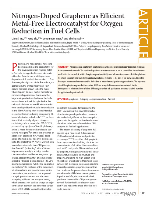
Although CNTs and their N-doped counterparts have been synthesized and studied for some years,the large-scale preparation of graphene sheets by chemical vapor deposition(CVD)is only the recent development.17,18More recently,attempts have been quartz purging min. furnaceFigure1.(a)A digital photo image of a transparent N-graphenefilmfloating on water after removal of the nickel layer by dissolving in an aqueous acid so-lution;(b,c)AFM images of the N-graphenefilm and the correpsonding height analyses along the lines marked in the AFM image(c1؊c3in panel c).Figure2.TEM and Raman analyses of the N-graphenefilms.(a)Low-magnification TEM image showing a few layers of the CVD-grown N-graphenefilm on a grid.Inset shows the correspondingelectron diffraction pattern.(b؊d)High magnification TEM imagesshowing edges of the N-graphenefilm regions consisting of(b)2,(c)4,and(d)ca.4؊8graphene layers.(e)The corresponding Ramanspectra of the N-graphenefilms of different graphene layers on aSiO2/Si substrate(Methods).XPS survey for the as-synthesized N-graphene shows the high-resolution N1s spectrum.the C-graphene suggests a stronger O2the former,an additional advantage asRRDE voltammograms for the ORR in air-saturated0.1M KOH at the C-graphene electrode(red line), line),and N-graphene electrode(blue line).Electrode rotating rate:1000rpm.Scan rate:0.01V/s.Mass Mass(N-grapene)؍7.5g.(b)Current density(j)؊time(t)chronoamperometric responses obtained at theN-graphene(square line)electrodes at؊0.4V in air saturated0.1M KOH.The arrow indicates the addition methanol into the air-saturated electrochemical cell.(c)Current(j)؊time(t)chronoamperometric response and N-graphene(square line)electrodes to CO.The arrow indicates the addition of10%(v/v)CO into KOH at؊0.4V;j o defines the initial current.(d)Cyclic voltammograms of N-graphene electrode inbefore(circle line)and after(square line)a continuous potentiodynamic swept for200000cycles at Scan rate:0.1V/s.。
氮磷共掺杂三维石墨烯的制备及其电化学性能的研究

氮磷共掺杂三维石墨烯的制备及其电化学性能的研究CHENG Xiao-yu;SONG Wei-ming;SUN Li【摘要】有机元素共掺杂能有效改善碳材料的电容性能.通过氮、磷共掺杂合成了三维石墨烯(N/P-G)电极材料.通过XRD、SEM、TEM、XPS等对样品微观结构和表面物性进行了表征.结果表明,当掺杂氮含量为7.03%,磷含量为4.62%,所合成N/P-G的比表面积可达156.138 m2·g-1,其平均孔径为4.45 nm,同时具有三维多孔结构.电化学性能研究表明,在1A·g-1电流密度下比电容高达145.4F·g-1,在16A·g-1电流下比电容仍可保持100.8F·g-1.所制备的氮磷共掺杂石墨烯作为电极材料可以应用于超级电容器中,前景良好.【期刊名称】《齐齐哈尔大学学报(自然科学版)》【年(卷),期】2019(035)004【总页数】6页(P40-45)【关键词】石墨烯;三维结构;共掺杂;超级电容器【作者】CHENG Xiao-yu;SONG Wei-ming;SUN Li【作者单位】【正文语种】中文【中图分类】O613.71;TM53石墨烯以独特的二维结构,大的比表面积和优良的传导性能作为超级电容器的电极材料被广泛报道[1]。
但石墨烯作为双电层电极材料,比电容较小,限制了其应用空间。
一般通过以下多种方法提高石墨烯的电化学性能:如生成多孔石墨烯来提高其比表面积[2-4];通过掺杂提高电化学性能[5-7]。
而用于掺杂的有机元素多为N,研究表明。
通过N原子的渗入可以大幅度提高储能过程中必不可少的碳基电导率和化学反应性[8-9]。
进一步的研究发现,除了N原子,其他非金属元素(B、P、S)的掺杂都有助于提高材料的电化学性能。
并且通过多元素共掺杂可以改善单杂原子掺杂引发的缺陷,研究表明多元素协同作用可以在石墨烯表面通过诱导形成高的局域电荷(自旋密度)而使其电化学性能显著提高。
不同种类氮掺杂石墨烯催化氧还原-氧析出反应的理论研究

不同种类氮掺杂石墨烯催化氧还原-氧析出反应的理论研究摘要:本文对不同种类氮掺杂石墨烯催化氧还原/氧析出反应的理论研究进行了探讨。
首先,介绍了石墨烯和氮掺杂石墨烯的基本概念和应用。
然后,通过对氮原子掺杂位置的调控,研究了以氧还原反应和氧析出反应为代表的氧化还原反应机理,并探讨了氮掺杂石墨烯在催化这些反应中的作用机理和性能指标。
最后,总结了不同种类氮掺杂石墨烯在催化氧化还原反应中的优缺点,并对未来的研究方向进行了展望。
关键词:石墨烯,氮掺杂,氧化还原反应,氧还原反应,氧析出反应,反应机理,作用机理,性能指标,优缺点1.引言石墨烯是一种单层碳原子构成的二维材料,具有优异的物理和化学性质,引起了广泛的研究关注。
氮掺杂石墨烯的引入,可以改善其化学和物理性质,提高催化性能和电化学储能性能,具有重大的实用价值。
氧还原反应和氧析出反应是一类重要的氧化还原反应,是化学、能源和材料领域中的关键反应之一。
在电化学能量转换和储存、燃料电池、生物传感器等方面都有广泛应用。
本文将从理论角度,研究不同种类氮掺杂石墨烯催化氧还原/氧析出反应的性能和机理。
2.石墨烯和氮掺杂石墨烯的基本概念和应用石墨烯是一种由碳原子组成的平面晶体,是最薄的二维材料之一。
其高表面积、独特的电子结构、高导电性和热导性等物理性质,使其在材料、电子器件、催化和能源方面有广泛的应用。
氮掺杂石墨烯是一种采用氮原子替代碳原子的材料,可以改变石墨烯的电荷输运性质和催化性质。
氮掺杂石墨烯的制备方法包括化学气相沉积、化学还原、电化学还原等。
氮原子的掺杂位置和类型对其性质产生重要影响,常见的氮掺杂方式有杂原子取代、吸附和浸渍等。
3.氧还原反应和氧析出反应的反应机理氧还原反应和氧析出反应是一类重要的氧化还原反应。
在这两种反应中,氧化剂和还原剂通过电子转移产生氧化和还原作用。
以氧还原反应为例,其反应方程式为:O2 + 4H+ + 4e- → 2H2O2H+ + 2e- → H2其反应机理可概括为:氧化反应:2H+ + O2 + 2e- → H2O2还原反应:H2O2 + 2e- → 2OH-氧析出反应是一种燃料电池中的重要反应,其反应方程式为:2H2O → O2 + 4H+ + 4e-其反应机理包括:水的分解反应:2H2O → 2H2 + O2氧气的还原反应:O2 + 4H+ + 4e- → 2H2O4.氮掺杂石墨烯在催化氧影响的机理和性能指标氮掺杂石墨烯在催化氧还原反应和氧析出反应中广泛应用。
N、B共掺杂MXene复合材料的制备及其电化学性能研究

N、B共掺杂MXene复合材料的制备及其电化学性能研究孙贺雷;李云飞;易荣华;王若冲;周爱军;孙义民【摘要】通过对Ti3A1C2 MAX相陶瓷粉进行刻蚀、插层、超声处理,制备出片状Ti3C2Tx MXene.以离子液体1-丁基-3-甲基咪唑四氟硼酸盐作为杂原子掺杂的氮源和硼源,通过不同温度热处理,得到新型的N、B掺杂MXene(N,B-Ti3C2Tx)作为超级电容器的电极材料.考察了煅烧温度对其电容性能的影响,结果表明,最佳煅烧温度为300℃,此时电容性能得到有效提高.在扫描速率为100mV/s时测得N,B-Ti3C2Tx-300℃的质量电容为65 F/g,是相同条件下Ti3C2Tx电容的5.5倍.EIS结果表明,N,B-Ti3C2Tx-300℃的接触电阻为0.52 Ω.循环稳定性测试表明,当电流密度为2 A/g时,充放电循环1000次后的电容保持率为84%.【期刊名称】《储能科学与技术》【年(卷),期】2019(008)001【总页数】8页(P130-137)【关键词】MXene;离子液体;氮硼共掺杂;电容性能【作者】孙贺雷;李云飞;易荣华;王若冲;周爱军;孙义民【作者单位】武汉工程大学材料科学与工程学院,等离子体化学与新材料湖北省重点实验室,湖北武汉430205;武汉工程大学材料科学与工程学院,等离子体化学与新材料湖北省重点实验室,湖北武汉430205;武汉工程大学材料科学与工程学院,等离子体化学与新材料湖北省重点实验室,湖北武汉430205;武汉工程大学材料科学与工程学院,等离子体化学与新材料湖北省重点实验室,湖北武汉430205;武汉工程大学材料科学与工程学院,等离子体化学与新材料湖北省重点实验室,湖北武汉430205;武汉工程大学材料科学与工程学院,等离子体化学与新材料湖北省重点实验室,湖北武汉430205【正文语种】中文【中图分类】TM53近年来,二维材料以其巨大的表面积、柔性的层状通道和可调控的电子结构在超级电容器领域展现出了巨大的应用潜力和广阔的发展前景[1-2]。
- 1、下载文档前请自行甄别文档内容的完整性,平台不提供额外的编辑、内容补充、找答案等附加服务。
- 2、"仅部分预览"的文档,不可在线预览部分如存在完整性等问题,可反馈申请退款(可完整预览的文档不适用该条件!)。
- 3、如文档侵犯您的权益,请联系客服反馈,我们会尽快为您处理(人工客服工作时间:9:00-18:30)。
The single layer graphene was grown on 34 mm Cu foils (99.95% purity, Goodfellow, UK) by low pressure CVD using ethylene (C2H4) and hydrogen (H2) as gas source. The Cu foil was heated up and annealed at 900 C for 30 min in the flowing 10 sccm H2 at 1 Torr. The gas mixture of H2 and C2H4 was then flowed at 4.6 Torr with a rate of 30 sccm and 10 sccm for 30 min, respectively. After the growth, the samples were cooled down to room temperature with flowing H2 under the pressure of 1 Torr. For the growth of CNx-graphene, NH3 diluted in He (NH3/He, v/v 10%) with the flow rate of 3–12 sccm was introduced into the reactor during the graphene growth process without changing the flow rates of H2 and C2H4. With (NH4)2S2O8 (0.1 M) as Cu etchant, the graphene or CNx graphene on Cu foils was transferred onto the Si wafer substrate with 285 nm SiO2 cap layer for Raman spectroscopy and contrast spectroscopy characterizations
Fig. 1 (a) Raman spectrum of the CVD graphene; the inset shows the contrast spectra of the CVD graphene on 300 nm SiO2/Si substrate. (b) Raman spectra of the CNx graphene synthesized with the NH3/He flow rate of 3 sccm (GN3). The N-doping greatly enhances the defect density in the CNx graphene as shown by the strong D band in Fig. 1b. The distribution of defects (incorporated N) in the N-doped graphene is inhomogeneous. Commonly the intensity ratio of D band to G band (ID/IG) has been used to evaluate the defect densitcontrast spectroscopy were performed on a WITEC CRM200 Raman system using a 100x objective lens with a numerical aperture (NA) of 0.95. The excitation source for Raman spectroscopy was a 532 nm laser (2.33 eV) with a laser power below 1 mW to avoid laser-induced heating. The illumination source for the contrast spectroscopy was normal white light. For Raman imaging, the sample was placed on an X–Y piezo-stage and scanned under the illumination of laser light with a step size of 250 nm. XPS and UPS studies of the graphene/CNx graphene on Cu foilswere performed using ESCALAB 250 (Thermo VGScientific). For theXPS analysis,monochromatic Al Ka(hn¼ 1486.6 eV) excitation was employed. For the UPS analysis, a He lamp was used with 21.2 eV (He I) and 40.8 eV (He II) excitation energies. TOF-SIMS study of the CNx graphene on Cu foils was performed on TOF-SIMS5 (ION-TOF GmbH) using 50 KeV Bi3 ++ as ion beam.The lateral resolution for SIMS imaging is 100 nm. For electrochemical measurements, two layers of graphene/CNx graphene were transferred onto the glassy carbon (GC) disk electrode (5 mm in diameter, Eco Chemie, Netherlands) through the layer by layer transfer method.12 The electrodes were dried at 60 C for 120 min. Oxygen reduction reaction (ORR) voltammograms were recorded using an Autolab potentiostat (Eco Chemie BV) with a three-electrode system in an oxygen saturated 0.1 M KOH (pH 13) electrolyte solution. The graphene/CNxgraphene on the glassy carbon rotating disk electrode (RDE) was used as a working electrode, with the rotating rate varying from 250 rpm to 2000 rpm. An Ag/AgCl electrode was used as a reference electrode and Pt sheet was used as a counter electrode.
The deliberate introduction of dopants into graphene could offer a possible route to tailor its electronic band structure, which is of great technological importance for its potential applications in nanoelectronics, nanophotonics, sensor devices, and green energy technology. Theoretical studies show that the N substitutional doping can modulate the band structure of graphene without impeding its good conducting behavior. In this work, we demonstrate the synthesis of N-doped single layer graphene (CNx graphene) with N percentage up to 16% by thermal chemical vapour deposition (CVD) of hydrogen (H2) and ethylene (C2H4) on Cu foils in the presence of ammonia. The chemical components and electronic structures of the as synthesized CNx graphene were characterized by Raman spectroscopy, time-of-flight secondary ion mass spectrometry , X-ray photoelectron spectroscopy (XPS), and ultraviolet photoemission spectroscopy (UPS) .The electronic structure characterization indicates the incorporated N is in pure pyridinic N–C bonding configuration. Since graphene layers doped by nearly pure graphitic N were previously synthesized by pyrolysis of methane (CH4) and NH3 on Cu foils, controllable N doping in graphene makes graphene an excellent platform for studying the doping effect of pure pyridinic/graphitic N on thephysical and chemical properties, such as electron and phonon transport properties, optical properties, and chemical activity.