GC0329 Application Notes_V1.0_Released_20110901
EFM32外设模块—OPAMP V1.10
目录1. 适用范围................................................................................. 错误!未定义书签。
2. 原理概述................................................................................. 错误!未定义书签。
3. 开发环境................................................................................. 错误!未定义书签。
4. 技术实现................................................................................. 错误!未定义书签。
5. 参考资料................................................................................. 错误!未定义书签。
6. 免责声明................................................................................. 错误!未定义书签。
1. 概述运算放大器(Operational Amplifier,简称OPAMP)是EFM32系列微控制器片上模拟外设,经过恰当地选取外部元件,它能够实现各种模拟运算,如放大、加、减、微分和积分等。
EFM32芯片内拥有三个运算放大器(Gecko系列芯片内部没有运算放大器),分别为OPA0、OPA1和OPA2。
其中OPA0和OPA1是DAC模块的一部分,OPA2为独立的运算放大器。
OPAMP模块框图如图1.1所示。
图1.1 OPAMP模块框图这三个运算放大器可以相互配合并通过搭配合适的外部电路和内部反馈满足复杂的应用需求。
Training Process ESEC 2009SSI Level 3 中文版

Presentation Name
company confidential
Page 19
Machine working principle 机器工作原理
特点 Single or dual wire mode Fully motorized in X, Y, Z Solder wire diameter range
Welcome to the World of
Soft Solder Process Training 2009SSI
Softsolder Technology
Time Planning
09:00AM – 09:30AM 09:30AM – 10:00AM 10:30AM – 10:45AM 10:45AM – 11:15AM 11:15PM – 12:00PM 13:30PM – 14:30PM 14:45PM – 15:00PM 15:00PM – 17:00PM
Page 4
<Name Presentaion>
Presentation Name
company confidential
Page 4
Machine Overview
Page 5
<Name Presentaion>
Presentation Name
company confidential
Page 5
Flow of Material材料流程
Leadframe 框架
Solder wire 焊锡丝
Wafer晶元
Die Bonded Leadframes Loaded in magazine 粘有芯片的框架装载 入料盒中
Page 8
<Name Presentaion>
PacketShaper_Product_Update,_November_2010.9

© Blue Coat Systems, Inc. 2010. All Rights Reserved.
Agenda
Value Framework New Product Announcements
• PacketShaper 8.6 • IntelligenceCenter 3 • PacketShaper 12000
PS 8.6: Classify by URL Category
WebPulse
Category Request Request Web Server
Content
1. 2. 3. 4. 5.
PacketShaper Sees Request Checks Local Cache Queries WebPulse Cloud Retrieves Category Applies Policy
5
© Blue Coat Systems, Inc. 2010. All Rights Reserved.
…but No One Owns the Web
HTTP
SSL
Web Applications and Content: Range from Inappropriate to Important They all look the same Potential for Performance Problems Defy traditional classifications
Web Awareness Billions
HTTP
PacketShaper
Today
Competitive View
Millions
Yesterday
Competition
GS93008
BMW Group Standard GS93008--12012--11Deskriptoren:Deklarationspflichtige Stoffe,gefährliche Stoffe,Inhaltsstoffe,verbotene Stoffe Ersatz fürGS93008--1:2009--07Descriptors:Declarable substances,substances of concern,constituents,prohibited substances Replacement forGS93008--1:2009--07Gefährliche StoffeWerkstoffe und BauteileVerbotene und deklarationspflichtige StoffeSubstances of concernMaterials and componentsProhibited and declarable substancesAusdrucke unterliegen nicht demÄnderungsdienst.Print-outs are not subject to the change service.Fortsetzung Seite2bis4Continued on pages2to4BMW AG Normung:80788MünchenE BMW AG interleaf-doc Alle Rechte vorbehalten/All rights reserved Bearbeiter/Editor:Christoph RaabeSeite/Page2GS93008--1:2012--11In case of dispute the German wording shall be valid. Vorwort ForewordDieser Group Standard wurde mit den verantwortlichen Bereichen der BMW Group abgestimmt.This Group Standard has been coordinated with the responsible departments of the BMW Group.Änderungen AmendmentsGegenüber GS93008-1:2009-07wurden folgendeÄnderun-gen vorgenommen:The following amendments have been made to GS93008--1:2009--07:--Titel geändert;--title changed;--zitierte Normen aktualisiert;--cited standards updated;--letzter Absatz in Abschnitt4gelöscht;--last passage in section4deleted; --Norm redaktionellüberarbeitet.--standard editorially revised.Frühere Ausgaben Previous editionsBMWN(S)11389.0--1:1997--12,1999--08GS93008--1:2002--07,2005--11,2008--03,2009--07BMWN(S)11389.0--3:1997--12GS93008--3:2002--071Anwendungsbereich1ScopeDieser Group Standard,in Verbindung mit der VDA232--101, dient Lieferanten,Herstellern und allen BMW-Fachstellen als Instrument zur Optimierung der Umweltverträglichkeit von Produkten und hilft bei der Prüfung von alternativen Stoffen.This Group Standard,along with VDA232--101serves suppliers,manufacturers and all BMW specialist departments as an instrument for the optimization of the environmental compatibility of products and assists in the testing of alternative substances.Der Group Standard entbindet Zulieferer und Verarbeiter aber nicht von der Pflicht,alle nationalen und internationalen gesetzlichen Regelungenüber gefährliche Stoffe und daraus resultierende Verbotsverordnungen einzuhalten.The Group Standard does not,however,relieve suppliers and processors from their obligation to comply with all national and international legal regulations regarding hazardous substances and prohibitory regulations resulting therefrom.Der Lieferant von Werkstoffen und/oder Bauteilen ist verpflichtet alle Registrierungs-und Meldepflichten für Erzeugnisse gemäßder Verordnung1907/2006(REACh)zu erfüllen.The suppliers of materials and/or components are obliged to fulfill all registration and reporting responsibilities for materials according to regulation1907/2006(REACh).Seite/Page3GS93008--1:2012--11 2Normative Verweisungen2Normative referencesDiese Norm enthält Festlegungen aus anderen Publikatio-nen.Diese normativen Verweisungen sind an den jeweiligen Stellen im Text zitiert und die Publikationen sind nachstehend aufgeführt.Es gilt die letzte Ausgabe der in Bezug genomme-nen Publikation.This Standard incorporates provisions from other publications.These normative references are cited at the appropriate places in the text and the publications are listed hereafter.The respective latest edition of the publication is applicable.GS93008--4Gefährliche Stoffe;Grenzwerte für Inhalts-stoffe und deren Emissionen in Werkstoffenund Bauteilen GS93008--4Substances of concern;Limit values for constituents and their emissions in materialsand componentsVDA231--106Werkstoff-Klassifizierung im Kraftfahrzeug-bau;Aufbau und Nomenklatur VDA231--106Material classification in motor vehicle construction;Structure and nomenclatureVDA232--101Globale Liste für deklarationspflichtige Stoffe im Automobilbau VDA232--101Global automotive declarable substance list (GADSL)GADSL1)Global Automotive Declarable Substance List GADSL1)Global Automotive Declarable Substance List1907/20062)Verordnung(EG)Nr.1907/2006des Europäi-schen Parlaments und des Rates vom18.De-zember2006zur Registrierung,Bewertung,Zulassung und Beschränkung chemischerStoffe(REACH),zur Schaffung einer Europäi-schen Chemikalienagentur,zurÄnderung derRichtlinie1999/45/EG und zur Aufhebung derVerordnung(EWG)Nr.793/93des Rates,derVerordnung(EG)Nr.1488/94der Kommis-sion,der Richtlinie76/769/EWG des Ratessowie der Richtlinien91/155/EWG,93/67/EWG,93/105/EG und2000/21/EG derKommission 1907/20062)Regulation(EC)No1907/2006of theEuropean Parliament and of the Council of18December2006concerning the Registration,Evaluation,Authorisation and Restriction ofChemicals(REACH),establishing aEuropean Chemicals Agency,amendingDirective1999/45/EC and repealing CouncilRegulation(EEC)No793/93and CommissionRegulation(EC)No1488/94as well asCouncil Directive76/769/EEC andCommission Directives91/155/EEC,93/67/EEC,93/105/EC and2000/21/EC3Verbotene und deklarationspflichtige Stoffe3Prohibited and declarable substancesFür BMW Produkte gilt die VDA232--101.Sie entspricht der Global Automotive Declarable Substance List (GADSL).VDA232--101applies to BMW products.It corresponds to the Global Automotive Declarable Substance List (GADSL).In der VDA232--101sind Stoffe und Stoffklassen zusammen-gestellt,die nach den heutigen Erkenntnissen potentielle Risi-ken für Mensch und Umwelt darstellen.The VDA232--101names substances and classes of substances that contain a potential risk for persons and for the environment.Die Dokumentation der Stoffe der VDA232--101erfolgt im Materialdatenblatt des entsprechenden Teils im Internationa-len Material-Daten-System IMDS(). Weiterhin ist eine Eingabe der Werkstoffklassen aus VDA 231--106und deren Anwendungscodes erforderlich.Documentation of substances of VDA232--101shall be carried out in the material data sheet for the respective component in the International Material-Data-System IMDS ().In addition entering the material category from VDA231--106and its application code is required.Die Grundlagen für die Erstellung eines Materialdatenblattes sind in den IMDS Recommendation und den BMW-Hinweisen zur Erstellung von IMDS Materialdatenblättern für BMW3) festgelegt.Die Erstellung des Materialdatenblattes erfolgt entsprechend dem“VDA Band2-Sicherung der Qualität von Lieferungen”im Rahmen der Erstbemusterung und entspricht Punkt20der Anlagen des VDA Erstmusterprüfberichts.Basic principles for the preparation of a material data sheet are determined in the IMDS Recommendation and the BMW notes regarding the preparation of IMDS material data sheet for BMW3).Preparation of the material-data sheet shall be according to the“VDA Band2-Sicherung der Qualität von Lieferungen”(VDA Volume2-Ensuring the quality of supplies)within the scope of the initial sampling.It corresponds to item20of the annexes of the VDA Erstmusterprüfbericht(VDA Initial Sampling Report).Die Materialdatenblätter sind mindestens als”Preliminary MDS”rechtzeitig zur Typgenehmigung bis spätestens8Mo-nate vor Serie vorzulegen.Die”Preliminary MDS”sind zur Erstbemusterung in”Final MDS”zuüberführen.The material data sheets shall be submitted at least as “preliminary MDS”at the latest8month before series launch in accordance with the schedule for type approval.At initial sampling the“preliminary MDS”must be converted to“final MDS”._______________1)Siehe 2)Siehe www.umwelt--online.de/”umwelt--online Login”3)Hinweise zur Erstellung von IMDS Materialdatenblätternfür BMW:https://b2bpapp6.muc/protected/de/gdz/tech-nologien/to/dokumente/MDB_hinweise.pdf _______________1)See 2)See www.umwelt--online.de/”umwelt--online Login”3)Guidance for BMW suppliers on creation of IMDS data-sheets:https://b2bpapp6.muc/protected/de/gdz/techno-logien/to/dokumente/MDB_hinweise.pdfSeite/Page4GS93008--1:2012--114Abweichungen4DeviationsVariationen/Umstellungen der Produkte sind mit der zustän-digenFachabteilung abzustimmenund erforderngegebenen-falls eine Neubemusterung.Variations/alterations of products are to be agreed with the respective department and may require a new sampling inspection.Gesetzliche Regelungen mit einem angekündigten terminier-ten Verbot des Stoffeinsatzes sowie daraus resultierende Ver-botsverordnungen und Anwendungsbeschränkungen sind bereits bei der Entwicklung von Komponenten einzuhalten, auch wenn das Stoffverbot erst nach Serieneinsatz in Kraft tritt.Legal regulations with an announced and scheduled prohibition of a material and the resulting prohibition regulations and limits of application must be complied with already during component development,even though the material/substance prohibition may enter into force only after series launch.5Weitere Stoffe5Additional substancesZusätzliche Stoffe,deren Inhaltsstoffe und Emissionswerte der Kontrolle unterliegen,sind in GS93008--4aufgelistet.Die Grenzwerte sind einzuhalten.Additional substances of which the matter and the emission values are subject to monitoring are listed in GS93008--4.The limit values must be adhered to.。
MOC3023中文资料
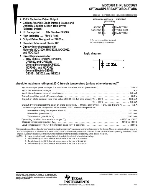
IMPORTANT NOTICETexas Instruments (TI) reserves the right to make changes to its products or to discontinue any semiconductor product or service without notice, and advises its customers to obtain the latest version of relevant information to verify, before placing orders, that the information being relied on is current.TI warrants performance of its semiconductor products and related software to the specifications applicable at the time of sale in accordance with TI’s standard warranty. Testing and other quality control techniques are utilized to the extent TI deems necessary to support this warranty. Specific testing of all parameters of each device is not necessarily performed, except those mandated by government requirements.Certain applications using semiconductor products may involve potential risks of death, personal injury, or severe property or environmental damage (“Critical Applications”).TI SEMICONDUCTOR PRODUCTS ARE NOT DESIGNED, INTENDED, AUTHORIZED, OR WARRANTED TO BE SUITABLE FOR USE IN LIFE-SUPPORT APPLICATIONS, DEVICES OR SYSTEMS OR OTHER CRITICAL APPLICATIONS.Inclusion of TI products in such applications is understood to be fully at the risk of the customer. Use of TI products in such applications requires the written approval of an appropriate TI officer. Questions concerning potential risk applications should be directed to TI through a local SC sales office.In order to minimize risks associated with the customer’s applications, adequate design and operating safeguards should be provided by the customer to minimize inherent or procedural hazards.TI assumes no liability for applications assistance, customer product design, software performance, or infringement of patents or services described herein. Nor does TI warrant or represent that any license, either express or implied, is granted under any patent right, copyright, mask work right, or other intellectual property right of TI covering or relating to any combination, machine, or process in which such semiconductor products or services might be or are used.Copyright © 1995, Texas Instruments Incorporated。
Verilog教程-夏宇闻(共178张)
第13页,共178页。
3.2 Verilog HDL基本(jīběn)结构
二、Verilog HDL模块的结构
▪ Verilog的基本设计单元是“模块 (block) ” 。 ▪ Verilog 模块的结构由在module和endmodule关键词
之间的4个主要部分组成:
1 端口定义 2 I/O说明
(3)用 “always” 块语句 结构说明语句
always @(posedge clk) // 每当时钟上升沿到来时执行一遍块内语句
begin
if(load)
out = data; // 同步预置数据 else
out = data + 1 + cin; // 加1计数
end
❖注1:“always” 块语句常用于描述时序逻辑,也可 描述组合逻辑。
3.12 不同抽象级别的Verilog HDL模型
1
3.13 设计技巧
第1页,共178页。
引言 3.1
(yǐnyán)
内容概要
一、什么是Verilog HDL 二、Verilog HDL的发展历史 三、不同层次的Verilog HDL抽象
四、Verilog HDL的特点
2
第2页,共178页。
3.1 引言(yǐnyán)
❖ Verilog HDL模块的模板(仅考虑用于逻辑综合的部分)
module <顶层模块名> (< 输入输出端口列表>) ;
output 输出端口列表;
input 输入端口列表;
//(1)使用assign语句定义逻辑功能
wire 结果信号名;
assign <结果信号名> = 表达式 ;
通用GVDP英文5版
Don Smith
22MAY06
This document is for internal GM use only. Not to be duplicated or disclosed outside GM without approval of Don Smith 586-986-1983
• Mainstream Architecture Configuration/Packaging
• Load path Strategy • Key Architectural BOM Rows Selected • Baseline Powertrain Plan (Engine/Trans. Families, Drive Types) • Proportional Model(s) • Sourcing Strategy • Manufacturing Strategy
5
GVDP v5_Upd_trg.ppt/Don Smith/5/22/2006/version 6.0
Pre-VPI GVDP Overview
No Architecture Modifications
(outside of bandwidth)
(e.g. GMX211,GMX272, GMX386)
GVDP Pre-VPI Process Documentation v1.0 Released 06MAR06
(for more information go to: /gvdp/pre_vpi.html )
GVDP Post DSI v5.0 Released 06April06
INDEX
4
GVDP v5_Upd_trg.ppt/Don Smith/5/22/2006/version 6.0
ADR292中文资料
VS = 5.0 V, 0 mA to 5 mA
ELECTRICAL SPECIFICATIONS (V = 2.7 V, T = ؊40؇C ≤ T ≤ +125؇C unless otherwise noted)
S
A
A
Parameter TEMPERATURE COEFFICIENT “E” Grade “F” Grade “G” Grade LINE REGULATION “E/F” Grades “G” Grade LOAD REGULATION “E/F” Grades “G” Grade SUPPLY CURRENT THERMAL HYSTERESIS
Symbol VO VOERR
2.048 2.050 +2 +0.10 2.048 2.051 +3 +0.15 2.048 2.054 +6 +0.29 30 40 30 40 50 6 420 100 125 100 125
VO VOERR
IOUT = 0 mA
VO VOERR ∆VO/∆VIN ∆VO/∆ ILOAD ∆VO eN eN
∆VO/∆VIN ∆VO/∆ ILOAD IS VO–HYS
2.7 V to 15 V, IOUT = 0 mA
VS = 5.0 V, 0 mA to 5 mA TA = +25°C –40°C ≤ TA ≤ +125°C SO-8, TSSOP-8 –2–
REV. B
Information furnished by Analog Devices is believed to be accurate and reliable. However, no responsibility is assumed by Analog Devices for its use, nor for any infringements of patents or other rights of third parties which may result from its use. No license is granted by implication or otherwise under any patent or patent rights of Analog Devices. One Technology Way, P.O. Box 9106, Norwood, MA 02062-9106, U.S.A. Tel: 781/329-4700 World Wide Web Site: Fax: 781/326-8703 © Analog Devices, Inc., 2001
HA3099
Timer0 CCP1
商标
Microchip 的名称和徽标组合、 Microchip 徽标、 Accuron、 dsPIC、 KEELOQ、 MPLAB、 PIC、 PICmicro、 PICSTART、 PRO MATE、 PowerSmart 和 rfPIC 均为 Microchip Technology Inc. 在美国和其它国家或地区的注册商 标。
3
RA2/AN2
4
RA3/AN3/VREF
5
RA4/T0CKI
6
RA5/AN4/SS
7
VSS
8
OSC1/CLKI
9
OSC2/CLKO
10
RC0/T1OSO/T1CKI
11
RC1/T1OSI/CCP2
12
RC2/CCP1
13
RC3/SCK/SCL
14
HA3099
28
RB7/PGD
27
RB6/PGC
26
• 4K x 14字闪存或ROM程序存储器,192 x 8字节数 据存储器 (RAM)
• 引脚配置与 PIC16F73/76 系列兼容 • 中断能力 (有 11 个中断源) • 八级深度硬件堆栈 • 直接寻址、间接寻址和相对寻址模式 • 处理器可以直接读取程序存储器
特殊单片机功能:
• 上电复位 (Power-on Rest, POR) • 上电延时定时器 (Power-up Timer, PWRT)和
机密
2004 Microchip Technology Inc.
CPLD IO User Guide
CPLD I/O User GuideUG445 (v1.1) November 27, 2007CPLD I/O User Guide UG445 (v1.1) November 27, 2007Xilinx is disclosing this Document and Intellectual Property (hereinafter “the Design”) to you for use in the development of designs to operate on, or interface with Xilinx FPGAs. Except as stated herein, none of the Design may be copied, reproduced, distributed, republished, downloaded, displayed, posted, or transmitted in any form or by any means including, but not limited to, electronic, mechanical,photocopying, recording, or otherwise, without the prior written consent of Xilinx. Any unauthorized use of the Design may violate copyright laws, trademark laws, the laws of privacy and publicity, and communications regulations and statutes.Xilinx does not assume any liability arising out of the application or use of the Design; nor does Xilinx convey any license under its patents, copyrights, or any rights of others. Y ou are responsible for obtaining any rights you may require for your use or implementation of the Design. Xilinx reserves the right to make changes, at any time, to the Design as deemed desirable in the sole discretion of Xilinx. Xilinx assumes no obligation to correct any errors contained herein or to advise you of any correction if such be made. Xilinx will not assume any liability for the accuracy or correctness of any engineering or technical support or assistance provided to you in connection with the Design.THE DESIGN IS PROVIDED “AS IS” WITH ALL FAULTS, AND THE ENTIRE RISK AS TO ITS FUNCTION AND IMPLEMENTA TION IS WITH YOU. YOU ACKNOWLEDGE AND AGREE THAT YOU HAVE NOT RELIED ON ANY ORAL OR WRITTEN INFORMA TION OR ADVICE, WHETHER GIVEN BY XILINX, OR ITS AGENTS OR EMPLOYEES. XILINX MAKES NO OTHER WARRANTIES, WHETHER EXPRESS, IMPLIED, OR STA TUTORY , REGARDING THE DESIGN, INCLUDING ANY WARRANTIES OF MERCHANTABILITY , FITNESS FOR A PARTICULAR PURPOSE, TITLE, AND NONINFRINGEMENT OF THIRD-P ARTY RIGHTS.IN NO EVENT WILL XILINX BE LIABLE FOR ANY CONSEQUENTIAL, INDIRECT, EXEMPLARY , SPECIAL, OR INCIDENTAL DAMAGES, INCLUDING ANY LOST DATA AND LOST PROFITS, ARISING FROM OR RELA TING TO YOUR USE OF THE DESIGN, EVEN IF YOU HAVE BEEN ADVISED OF THE POSSIBILITY OF SUCH DAMAGES. THE TOTAL CUMULA TIVE LIABILITY OF XILINX IN CONNECTION WITH YOUR USE OF THE DESIGN, WHETHER IN CONTRACT OR TORT OR OTHERWISE, WILL IN NO EVENT EXCEED THE AMOUNT OF FEES P AID BY YOU TO XILINX HEREUNDER FOR USE OF THE DESIGN. YOU ACKNOWLEDGE THAT THE FEES, IF ANY , REFLECT THE ALLOCATION OF RISK SET FORTH IN THIS AGREEMENT AND THAT XILINX WOULD NOT MAKE AVAILABLE THE DESIGN TO YOU WITHOUT THESE LIMITA TIONS OF LIABILITY .The Design is not designed or intended for use in the development of on-line control equipment in hazardous environments requiring fail-safe controls, such as in the operation of nuclear facilities, aircraft navigation or communications systems, air traffic control, life support, or weapons systems (“High-Risk Applications”). Xilinx specifically disclaims any express or implied warranties of fitness for such High-Risk Applications. Y ou represent that use of the Design in such High-Risk Applications is fully at your risk.© 2007 Xilinx, Inc. All rights reserved. XILINX, the Xilinx logo, and other designated brands included herein are trademarks of Xilinx, Inc. All other trademarks are the property of their respective owners.Revision HistoryThe following table shows the revision history for this document.DateVersion Revision 6/26/071.0Initial Xilinx release.11/27/07 1.1•Added “JTAG Termination,” page 12.•UpdatedFigure 4.•Added sentence at the end of first paragraph after Figure 5.CPLD I/O User Guide 3UG445 (v1.1) November 27, 2007Preface: About This GuideGuide Contents . . . . . . . . . . . . . . . . . . . . . . . . . . . . . . . . . . . . . . . . . . . . . . . . . . . . . . . . . . . . . . 5Additional Resources . . . . . . . . . . . . . . . . . . . . . . . . . . . . . . . . . . . . . . . . . . . . . . . . . . . . . . . . 5Additional Documentation . . . . . . . . . . . . . . . . . . . . . . . . . . . . . . . . . . . . . . . . . . . . . . . . . . . 5Conventions . . . . . . . . . . . . . . . . . . . . . . . . . . . . . . . . . . . . . . . . . . . . . . . . . . . . . . . . . . . . . . . . . 6Typographical. . . . . . . . . . . . . . . . . . . . . . . . . . . . . . . . . . . . . . . . . . . . . . . . . . . . . . . . . . . . . 6Online Document. . . . . . . . . . . . . . . . . . . . . . . . . . . . . . . . . . . . . . . . . . . . . . . . . . . . . . . . . . 7CPLD I/O User GuideTerminations . . . . . . . . . . . . . . . . . . . . . . . . . . . . . . . . . . . . . . . . . . . . . . . . . . . . . . . . . . . . . . . . .9Termination Options . . . . . . . . . . . . . . . . . . . . . . . . . . . . . . . . . . . . . . . . . . . . . . . . . . . . . . . 9Setting Termination Modes in Software. . . . . . . . . . . . . . . . . . . . . . . . . . . . . . . . . . . . . . 10Termination Mode for Outputs . . . . . . . . . . . . . . . . . . . . . . . . . . . . . . . . . . . . . . . . . . . . . 10Bus-hold/Keeper . . . . . . . . . . . . . . . . . . . . . . . . . . . . . . . . . . . . . . . . . . . . . . . . . . . . . . . . . 10Impedance of the Bus-hold, Keeper, or Pull-up . . . . . . . . . . . . . . . . . . . . . . . . . . . . . . . 11Half Latch . . . . . . . . . . . . . . . . . . . . . . . . . . . . . . . . . . . . . . . . . . . . . . . . . . . . . . . . . . . . . . . 11CoolRunner XPLA3 . . . . . . . . . . . . . . . . . . . . . . . . . . . . . . . . . . . . . . . . . . . . . . . . . . . . 11CoolRunner-II . . . . . . . . . . . . . . . . . . . . . . . . . . . . . . . . . . . . . . . . . . . . . . . . . . . . . . . . . 12XC9500, XC9500XL, and XC9500XV . . . . . . . . . . . . . . . . . . . . . . . . . . . . . . . . . . . . . . . . 12JTAG Termination . . . . . . . . . . . . . . . . . . . . . . . . . . . . . . . . . . . . . . . . . . . . . . . . . . . . . 12Thresholds . . . . . . . . . . . . . . . . . . . . . . . . . . . . . . . . . . . . . . . . . . . . . . . . . . . . . . . . . . . . . . . . . . 12I/V Curves . . . . . . . . . . . . . . . . . . . . . . . . . . . . . . . . . . . . . . . . . . . . . . . . . . . . . . . . . . . . . . 12Reading I/V Curves . . . . . . . . . . . . . . . . . . . . . . . . . . . . . . . . . . . . . . . . . . . . . . . . . . . . 13Maximum I/O Power Dissipation . . . . . . . . . . . . . . . . . . . . . . . . . . . . . . . . . . . . . . . . . 15Drive Strength . . . . . . . . . . . . . . . . . . . . . . . . . . . . . . . . . . . . . . . . . . . . . . . . . . . . . . . . . . . 16Power, Sequencing, and Slew Rates . . . . . . . . . . . . . . . . . . . . . . . . . . . . . . . . . . . . . . . . . 17Hot-Swappable. . . . . . . . . . . . . . . . . . . . . . . . . . . . . . . . . . . . . . . . . . . . . . . . . . . . . . . . . . . 17Powering CPLDs . . . . . . . . . . . . . . . . . . . . . . . . . . . . . . . . . . . . . . . . . . . . . . . . . . . . . . . . . 17Power Sequencing . . . . . . . . . . . . . . . . . . . . . . . . . . . . . . . . . . . . . . . . . . . . . . . . . . . . . . 17Current Consumption . . . . . . . . . . . . . . . . . . . . . . . . . . . . . . . . . . . . . . . . . . . . . . . . . . . . . 205V Tolerance . . . . . . . . . . . . . . . . . . . . . . . . . . . . . . . . . . . . . . . . . . . . . . . . . . . . . . . . . . . . . 20I/O Standards. . . . . . . . . . . . . . . . . . . . . . . . . . . . . . . . . . . . . . . . . . . . . . . . . . . . . . . . . . . . 22Simultaneous Switching Output Limits . . . . . . . . . . . . . . . . . . . . . . . . . . . . . . . . . . . . . . 22Decoupling Guidelines . . . . . . . . . . . . . . . . . . . . . . . . . . . . . . . . . . . . . . . . . . . . . . . . . . . . 22Schmitt Trigger. . . . . . . . . . . . . . . . . . . . . . . . . . . . . . . . . . . . . . . . . . . . . . . . . . . . . . . . . . . 22Slew Rate . . . . . . . . . . . . . . . . . . . . . . . . . . . . . . . . . . . . . . . . . . . . . . . . . . . . . . . . . . . . . . . . 23Table of Contents CPLD I/O User GuideUG445 (v1.1) November 27, 2007Preface About This GuideThe CPLD I/O User Guide describes the behavior of the I/Os under various operatingconditions. It describes how to use the different termination modes, how to understandthresholds, and how loading affects the I/Os.Guide ContentsThis manual contains the following topics:•“Terminations” provides a brief description of the different terminations available inXilinx CPLDs. It also contains details on how to use termination.•“Thresholds” describes in detail the conditions that affect the threshold levels. It givesexamples on how to use the I/V curves to understand what thresholds will be undernominal operating conditions.•“Power, Sequencing, and Slew Rates” describes effects of powering, sequencing, andslew rates on I/Os. It includes details on how much voltage can be driven into aXilinx CPLD and the behavior of the I/Os in different operating conditions.Additional ResourcesTo find additional documentation, see the Xilinx Web site at:/support/documentation/index.htm.To search the Answer Database of silicon, software, and IP questions and answers, or tocreate a technical support WebCase, see the Xilinx Support Web site at:/support.Additional DocumentationXilinx ISE Software Manuals are available for download at:/support/software_manuals.htm.The following documents are also available:•DS012CoolRunner™ XPLA3 CPLD Data SheetThis data sheet contains the electrical and functional specifications of the CoolRunnerXPLA3 CPLD.•DS090CoolRunner-II CPLD Family Data SheetThis data sheet contains the electrical and functional specifications of theCoolRunner-II CPLD.CPLD I/O User Guide 5 UG445 (v1.1) November 27, 2007 CPLD I/O User GuideUG445 (v1.1) November 27, 2007•DS054 XC9500XL High-Performance CPLD Family Data SheetThis data sheet describes the XC9500XL 3.3V CPLD Family, including architecture,basic family device descriptions, and package options.•DS049 XC9500XV High-Performance CPLD Family Data Sheet *This data sheet describes the XC9500XV 2.5V CPLD Family, including architecture,basic family device descriptions, and package options.*Please note that this family has been discontinued and is not recommended for use innew designs. For further information, please see XCN07010.•UG112 Device Package User GuideThis guide discusses thermal, electrical, moisture, and soldering characteristics ofXilinx device packages.•XAPP150 I/V Curves for Xilinx FPGA and CPLD FamiliesThis application note describes the output sink and source current for averageprocessing, nominal supply voltage, and room temperature.•XAPP342 XPLA3 I/O Cell Characteristics Application NoteThis application note describes the features and benefits of the I/O cells provided byXilinx CoolRunner XPLA3 CPLDs.•XAPP382 CoolRunner-II I/O Characteristics Application NoteThis document is a comprehensive description of the I/O structure of theCoolRunner-II CPLD family.•XAPP429 5V Tolerance Techniques for CoolRunner-II Devices Application NoteThis application note describes several different methods for interfacing 5V signals toCoolRunner-II devices.ConventionsThis document uses the following conventions. An example illustrates each convention.T ypographicalThe following typographical conventions are used in this document:ConventionMeaning or Use Example Courier font Messages, prompts, andprogram files that the systemdisplaysspeed grade: - 100Courier bold Literal commands that you enter in a syntactical statementngdbuild design_nameItalic fontReferences to other manuals See the Development System Reference Guide for moreinformation.CPLD I/O User Guide 7UG445 (v1.1) November 27, 2007Online DocumentThe following conventions are used in this document:Convention Meaning or UseExample Blue text Cross-reference link to alocation in the currentdocument See the section “Additional Resources” for details.In the example in Figure 2, ifthe Volmax is 0.5V , you cansink 21 mA.Blue, underlined text Hyperlink to a website (URL)Go to for the latest speed files. CPLD I/O User GuideUG445 (v1.1) November 27, 2007CPLD I/O User GuideTerminationsTerminations are a vital aspect of a robust transmission line. The on-chip termination ofthe CPLD I/Os eliminate the need for external termination. It is strongly recommendednot to float CMOS inputs as this increases power. The on-chip termination of the CPLDscan be used to minimize power without the need for external components. The followingsection will discuss the termination options available in the different CPLD families andhow to utilize the features.T ermination OptionsThe user can select the termination type for the unused I/Os and the Input and TristateI/Os separately.For the Input and Tristate I/O termination mode, the options are (default in parentheses):Note:Bus-hold and Keeper terms can be used interchangeably.•XC9500 XL/ XV: Float, Keeper (keeper)•CoolRunner™ XPLA3: Float, Pull-up (pull-up)•CoolRunner-II: Float, Pull-up, Keeper (Keeper)For the Unused I/Os, the options are (default in parentheses):•XC9500 /XL/XV: Float, Ground (float)•CoolRunner XPLA3: Float, Pull-up (pull-up)•CoolRunner-II: Float, Ground, Pull-up, Keeper (ground)For CoolRunner-II devices, it is possible to have a combination of multiple terminationmodes for used and unused I/Os. However, not all combinations are possible. Below arethe permitted combinations:Table 1:Input Termination SchemesPossible Input Termination SchemesAll Pull-upAll Bus-holdCombination of Pull-up and FloatCombination of Bus-hold and FloatAll FloatCPLD I/O User Guide 9 UG445 (v1.1) November 27, 2007Table 2:Unused I/O Termination SchemesUnused I/O Termination SchemesAll Pulled-up (not possible if Bus-hold is selectedfor input termination)All Bus-hold (not possible if Pull-up is selected forinput termination)All Configurable GroundAll FloatIt is not recommended to float a CPLD I/O, as it consumes extra current than if held in aknown state. You should select float as a termination mode only if the pin has externalterminations.Setting T ermination Modes in SoftwareThe termination modes can either be selected globally, as CPLDFit options, or on apin-by-pin basis using constraints.If you are using the ISE GUI:1.Select the top level in the Sources window.2.In the Processes window, select CPLDFit.3.Right-click and select Properties. The Fit Properties dialog box appears.There is a drop-down menu for the Input and Tristate I/O termination mode. For theCoolRunner-II and CoolRunner XPLA3, there is a drop-down menu for the Unused I/OPad termination. However, if the design targets an XC9500, XC9500XL, or XC9500XV,there are only two options for the unused termination; by default, this is float. The user hasthe option to Create Programmable Ground pins on Unused I/Os; if this check box isticked, the pin can be considered as outputs driving low.To constrain the termination on a pin-by-pin basis, use the following UCF example:NET "My_NET" KEEPER;For more information on the constraints syntax, see the Constraints Guide in the softwaremanuals, found at:/support/software_manuals.htm.T ermination Mode for OutputsIt is not possible or necessary to select a termination mode for output pins. The output of amacro cell, which drives the output, will always be at logic 1 or logic 0. Therefore, there isno need to terminate the output. Outputs that are in a Tristate condition can be terminated.Bus-hold/KeeperThe bus-hold or keeper is present in the CoolRunner-II, XC9500, XC9500XL, andXC9500XV families. It is internal circuitry that will drive the last known value on the I/Ointo the device. The bus-hold circuit is only on when the device is in user mode and keepertermination mode is selected. Therefore, if the device is unconfigured or in the CPLD I/O User GuideUG445 (v1.1) November 27, 2007Programming (ISP) mode, the bus-hold is not active. If the device loses V CCINT, the I/Oswill be in a pull-up state. The Bus-hold is enabled by Vccint, but pulls to Vccio.Impedance of the Bus-hold, Keeper, or Pull-upThe values given in this section are typical numbers that cannot be guaranteed as theimpedance varies over process, voltage, and temperature.CoolRunner-IIThe effective resistance of the termination circuitry varies with V CCIO.At V CCIO = 1.8V, the effective resistance is typically 100k Ohm.As V CCIO increases, the effective resistance decreases. Typical for V CCIO =3.3V is 42k Ohm.The minimum resistance value presented by the termination circuitry is 20k Ohm.CoolRunner XPLA3The CoolRunner does not have a bus-hold. It does have an internal pull-up that has beencharacterized at approximately 60k to 150k Ohms.XC9500, XC9500XL, and XC9500XVThe bus hold impedance is approximately 25k Ohm, with a range of 15K to 70K (the lowerrange at lower temperatures).Half LatchCoolRunner XPLA3The CoolRunner XPLA3 has a half latch feature on the I/Os. The half latch is essentially apull-up that turns on only when the I/O pin voltage is in the linear region (not a 0, not a 1).So, when the voltage at the pin is in the trip-point region or higher, the half latch will beenabled. The idea is that it will prevent signals from floating, and therefore, save power.This half latch cannot be disabled.The device data sheet states the following: “The I/O is configured as an input (or 3-statedoutput), a half latch feature exists. This half latch pulls the input high (through a weakpull-up) if the input should float and cross the threshold.”This means that the half latch feature exists even when the pull-up is not selected. If youwant to pull down the input, a resistor strong enough to overcome the half latch must beused. Xilinx recommends that any pull-down resistor value be 10k Ohms or less. Xilinxdoes not recommend using CoolRunner XPLA3 devices in any design that requires I/Opins to truly float.Some CoolRunner XPLA3 devices appear to have a pull-up on the I/O pins when there isno pull-up specified, this is due to the CoolRunner XPLA3 half latch circuitry. The range ofthe trip-point is from 0.9V to 1.6V. There was a change in the trip-point when Xilinxchanged fabs. The change in fab locations is documented in PCNs, and is available on theXilinx Customer Notices page:/support/documentation/customer_notices.htm.The trip-point for the newer devices (part marking of *MN) is lower than the trip-point forthe older devices (part marking of APN); this can result in the half latch circuitry being“turned on” sooner than in the older devices. If this occurs, a pull-down resistor of a valuestronger than 10K is required to overcome the half latch pull-up resistance; a value of 4.7kohm is recommended. If the incorrect value of a pull-down is used, a voltage divider willbe created at the input.More information on the half latch is available in the XPLA3 I/O Cell CharacteristicsApplication Note (XAPP342).CoolRunner-IIThe CoolRunner-II I/Os have a half latch feature enabled by default. Half latch occurs onlyin cases when the CoolRunner-II I/Os are configured as LVCMOS18 and the Schmitttrigger is disabled. If the Schmitt trigger is used, the half latch is disabled. When usingLVCMOS18, the only way to turn the half latch off is to enable the Schmitt trigger on thatinput.XC9500, XC9500XL, and XC9500XVThe XC9500 families do not have a half latch.The XC9500XL and XC9500XV have internal circuitries that function in a similar manner toa half latch. To overcome this circuitry, ensure that a pull-down of 4K7 ohm or stronger isused. (The effective resistance of the internal circuitry is between 30k - 60k Ohm.) JT AG T erminationXC9500, XC9500XL, XC9500XV, and CoolRunner XPLA3 have internal pull-ups on TDIand TMS.CoolRunner-II devices have internal pull-ups on TDI, TMS, and TCK.It is not necessary to externally terminate JTAG pins with internal termination; they can beleft floating. External pull-ups on pins with internal termination is allowed, but notnecessary. External pull-down termination is not recommended as it would conflict withthe internal pull-ups.ThresholdsI/V CurvesThe I/V curve is a graphical representation of the nominal amount of current that an I/Ocan source or sink at different voltage levels. The range of voltage levels, and therefore, thecurrent, is dependent on the I/O voltage used. The I/V curves provide details onthresholds.The I/V curves for the CoolRunner-II and CoolRunner XPLA3 devices can be found in thefamily data sheets and in the I/V Curves for Xilinx FPGA and CPLD Families Application Note(XAPP150) for the XC9500, XC9500XL and XC9500XV families.Questions often asked by users are:•How much current can an I/O source or sink?•If I am driving a certain load, what voltage levels can I expect? CPLD I/O User GuideReading I/V CurvesCustomers who need to understand what threshold their outputs will have can use the I/V curve (for example, if you are using an I/O standard powered at 3.3V, and need to know how much current can be sourced from the I/O). The threshold that the CPLD drives out can be determined by the Vihmin of the downstream device (i.e., if the downstream device requires a Vihmin of 3.0V, then you must ensure that the CPLD can drive out this voltage with its current loading). If the Vohmin is 3.0V, then you can extrapolate from the curve in Figure1; under typical conditions, the device can source 18 mA of current withoutdropping below the required threshold.UG445_01_052207Figure 1:I/V Curve Example 1If you want to find out how much current an I/O can sink before you raise the voltage levelabove Volmax, you can look at the Iol (output low current) curve in Figure2, the Volmaxand trace to the corresponding current value.In the example in Figure2, if the Volmax is 0.5V, you can sink 21 mA.UG445_02_052207Figure 2:I/V Curve Example 2Another common use of the I/V curve is to determine the voltage at the IOB depending onthe load.For example, if you are driving a 24 mA load from CPLD, will you violate the inputthresholds? CPLD I/O User GuideFrom the curve (see Figure 3), you can see that when you drive 24 mA, the nominal outputwill be 2.8V , which is above the Vohmin requirement for both the LVCMOS33 and LVTTLstandards.The user must ensure that the Vohmin requirement meets the Vihmin of the downstreamdevice.Maximum I/O Power DissipationAs an example, you might want to know how to calculate the maximum number of I/Osone device can sink or source before damaging the device.In this example, you will calculate how many I/Os one device can sink or source currentbefore you violate the acceptable Ta range. If you want to keep the device within therecommended limits to prevent long-term reliability implications, adjust the TjMax so thatit is equal to the maximum Ta for the temperature grade you are using (i.e., Commercial =70°C, Industrial = 85°C). This will ensure that the 20-year data retention limit is preserved,as well as guarantee the specified timing delays in the data sheet.If you sink or source lots of current with one device, you risk heating it so much that it isdestroyed. So, you need to know the maximum permissible temperature of the package. Ifyou want to perform the calculations to see how much current will be sourced or sunkbefore the device is compromised, adjust the Tjmax in the calculation to the Tjmax of thepackage (i.e., Tjmax = 125°C for a plastic package).Figure 3:I/V Curve Example 3UG445_09_101007Tjmax > (ThetaJC * Pd) + Ta-Where Tjmax = Tamax of 70°C-ThetaJC is available in the Device Package User Guide (UG112)-Pd is the power dissipated (use XPower, or measure the design power)-Ta is the ambient temperature at which the device will runFor example, if you want to know how many output loads you could drive that eachrequire 40 mA with one device, the selected device is XCR3064XL-PC44:-Tjmax is 70°C for a plastic package-ThetaJC is 12.4°C/Watt for PC44 package-Ta will not exceed 50°C70 = (12.4*Pd) + 50Pd = 1.613WYou will need to expand Pd to take into account Pd of the design and the I/O:(Pddesign + PdIO) = 1.613WPddesign is 66 mW from measurement; doubled to 132 mW for safety cushion.When sourcing 40 mA, the voltage at the output of the CPLD will be 2.3V (informationobtained from the I/V curve).(X*2.3V) = 1.613W - 0.132WX = 1.48W/2.3VX = 0.644AYou should have 644 mA to use to drive the I/O pins.644 mA/40 mA = 16 output loads can be driven by this device before you exceed theacceptable temperature range.How many 40 mA output loads can the device sink?When sinking 40 mA, the voltage at the output of the CPLD will be 0.7V.(X*0.7V) = 1.613W - 0.132WX = 1.481W/0.7VX = 2.12AYou should have 2116 mA to use to drive the I/O pins.2116 mA/40 mA = 53 LEDs can be driven by this device before before you exceed theacceptable temperature range.Drive StrengthYou cannot select the drive strength for CPLDs. The drive strength must be read from theI/V curve. CPLD I/O User GuidePower, Sequencing, and Slew RatesThe maximum voltage that you can you drive into an I/O with the device powered orunpowered, is limited to the Vi/Vin parameter in the family data sheet.•XC9500: You can drive into an unpowered I/O, provided Vin does not exceed the Vinlimits of the CPLD.•XC9500XL: You can drive into an unpowered I/O, provided Vin does not exceedV CCINT by more than 4.0V.•XC9500XV: You can drive into an unpowered I/O, provided Vin does not exceed theVin limits of the CPLD.•CoolRunner XPLA3: You can drive into an unpowered I/O, provided Vin does notexceed V CCINT by more than 4.0V.•CoolRunner-II: You can drive into an unpowered I/O, provided Vin does not exceed the Vin limits of the CPLD.In terms of current, the absolute maximum current that should be applied to anunpowered part is 100mA to the whole part.Before the device is configured and for unprogrammed devices, the status of the I/Os aredisabled and terminated with a weak pull-up.Hot-SwappableThe following list indicates whether or not devices are hot-swappable:•CoolRunner-II: Yes•CoolRunner XPLA3: Yes•XC9500XL: Yes•XC9500XV: Yes•XC9500: NoXC9500 has clamp diodes to V CC (5V); the XC9500XL, XC9500XV, CoolRunner XPLA3 andCoolRunner-II devices do not.Powering CPLDsSome of the CPLD families have multiple voltage rails. V CCINT supplies power to internallogic and to the configuration circuit. V CCIO only supplies power to I/O buffers. V CCAUXsupplies power to JTAG pins on the CoolRunner-II. In previous families the JTAG pinswere powered by V CCIO.CoolRunner-II CPLDs have three separate voltage rails: V CCINT, V CCIO, and V CCAUX.XC9500, XC9500XL, and XC9500XV have two separate voltage rails; V CCINT and V CCIO.Power SequencingCoolRunner-II devices are guaranteed to work under all power sequences. However, theorder in which V CCINT and V CCIO are applied might cause the CPLD to functiondifferently. V CCAUX can be powered at any time, independent of V CCINT and V CCIO.V CCINT and V CCIO are most important because they determine whether the CPLD logiccomes alive before the I/Os, or if the I/Os are to come alive before the CPLD logic.。
- 1、下载文档前请自行甄别文档内容的完整性,平台不提供额外的编辑、内容补充、找答案等附加服务。
- 2、"仅部分预览"的文档,不可在线预览部分如存在完整性等问题,可反馈申请退款(可完整预览的文档不适用该条件!)。
- 3、如文档侵犯您的权益,请联系客服反馈,我们会尽快为您处理(人工客服工作时间:9:00-18:30)。
4.1 Pixel Array 控制 ............................................... 8 4.2 时钟预分频 ..................................................... 9 4.3 输出时序说明及同步信号控制 . (9)
6.2 自动白平衡(Auto White Balance ) .............................. 16 6.3 镜头阴影补偿(Lens Shading Compensation ) ..................... 16 6.4 去坏点(Delete defective points ) .. (18)
6.5 去噪(Denoise) (19)
图3-1 外围连接参考
注:GC0329可与GC6103构成高性价比双摄像头设计方案,具体连接方式参见《GC0329
图3-2上电时序图
要恢复normal 工作模式,需要将0xfc[0]置0,0xf0写为0xff 。
3.3.3 输出使能控制
表3-2 输出驱动能力控制
原始图像镜像翻转垂直翻转镜像垂直翻转
图4-1 图像翻转控制
表4-2 内部分频设置1
一般分频的推荐设置如下表: 假设帧同步信号Vsync 低有效,行同步Hsync 为高有效,而输出格式为YCbCr 或RGB565图像的话,Vsync 和Hsync 的关系如下:
控制。
当exp_time > win_height+VB时,Bt=exp_time-win_height-St-Et。
帧率由exp_time决定。
下面是一行时间(row_time)的计算方法:
row_time = Hb + Sh_delay + win_width + 4。
表4-4 同步信号极性控制
2)Crop window模式。
下面给出几种常用subsample的设置。
(P0:0x5a表示0x5a寄存器是page0的,page选择由P0:0xfe[1:0]设置,设为0x00表示page0,设为0x01表示page1)
(P1:0x29[11:8],P1;0x2a )和Hb ({P0:0x05,P0:0x06}),Vb ({P0:0x07,P0:0x08}),exp_level(P1:0x2b~0x32)来实现。
消除flicker 的原理即是曝光时间是灯管周期的整数倍。
计算方法为: step * row_time = N * T
1)step 便是0x2a 要写入的值。
Exp_level2 { P1:0x2f[3:0], 0x30 } Exp_level3 { p1:0x31[3:0], 0x32 }
设置“一拖一”模式的工作步骤如下:
1、设置前摄像头使之工作在SPI出图模式,并具有合适的HB宽度,不打开输出使能。
2、在后摄像头(GC0329)出图的基础上,
由于绝大多数的镜头是球面系统,远离主光轴的光线穿过镜头时会产生衰减,因此,处于芯片四周的感光元件无法吸收全部的平行入射光线,体现在图像上便是图像四周的亮度比中心要暗。
LSC模块可以提高图像边缘区域像素点的增益,从而对图像四周的亮度进行补偿。
GC0329的LSC校正在一个标准直角坐标系内进行。
LSC_gain计算公式:=1 + a*x*y +
表6-4去坏点设置
注:1、要多去坏点,减小Dark threshold / Bright threshold;反之,则放大Dark threshold
/ Bright threshold 。
表6-5去噪设置
6.6 边缘加强(Edge Enhancement )
表6-8对比度设置
GC0329有两种gamma :RGB gamma 和Y gamma ,分别是在RGB 域和YUV 域上做Gamma ,可以共同使用。
GC0329 Application Notes
21 / 21
C32 = 1- C22- C12, C33 = 1- C23- C13,。