VA7204L2_DS_1[1].4_CH
CTC-ONU认证报文过程

牧马人的epon设备(插拔光纤时onu认证的报文)1、扩展发现OAMsend OAM:pkt len = 50, port = 0============================================================================== 00194264: 01 80 c2 00 00 02 00 1a ec 01 03 39 88 09 03 00 ; ...........9.... 00194274: 50 00 01 10 01 00 00 00 0e 05 ee 00 13 25 00 00 ; P............%.. 00194284: 00 00 02 10 01 00 00 00 0f 05 ee 00 13 25 00 00 ; .............%.. 00194294: 00 00 ; ................[000019ef:IGMP:0] mc tmr heartbeat[000019ef:APP:5] LOOPDETECT_TIMER_EXPIRED:port(255)[000019ef:APP:5] open port 1 period time out[000019ef:APP:3] vlan flooding ,dport 1, vlan count 0[000019ef:APP:5] open port 2 period time out[000019ef:APP:3] vlan flooding ,dport 2, vlan count 0[000019ef:APP:5] open port 3 period time out[000019ef:APP:3] vlan flooding ,dport 3, vlan count 0[000019ef:APP:5] open port 4 period time out[000019ef:APP:3] vlan flooding ,dport 4, vlan count 0[00001a0d:PTP:1] The tod_info is: $GPZDA001964000119700019.[00001a0d:PTP:0] update sys time 64633442256[00001a0d:PTP:4] trigger 1pps signal at time 65000000000(0xd224d4a0) [00001a0d:PTP:4] trigger tod info at time 65001000000(0xd225c8c4) Rcv OAM:pkt len = 60, port = 0============================================================================== 0014f068: 01 80 c2 00 00 02 00 e0 8e 88 01 00 88 09 03 00 ; ................ 0014f078: 50 00 01 10 01 00 00 00 0f 05 ee 00 13 25 00 00 ; P............%.. 0014f088: 00 00 02 10 01 00 00 00 0e 05 ee 00 13 25 00 00 ; .............%.. 0014f098:00 00 fe 07 11 11 11 01 21 00 00 00 ; ........!.......oam_ctc_build_pdu_infoLength=7+4x 07是最小值0x01:支持OAM扩展0x00:不支持OAM扩展ONU支持电信的版本号send OAM:pkt len = 57, port = 0==============================================================================001941d4: 01 80 c2 00 00 02 00 1a ec 01 03 39 88 09 03 00 ; ...........9....001941e4: 50 00 01 10 01 00 00 00 0e 05 ee 00 13 25 00 00 ; P............%..001941f4: 00 00 02 10 01 00 00 00 0f 05 ee 00 13 25 00 00 ; .............%.. 00194204: 00 00 fe 07 11 11 11 01 21 ; ........!.......[00001a33:APP:3] app_pkt_rx len 64 type 10 port 0[00001a37:OAM:0] oam_ind_oampdu(2、扩展的组织特定(Organization Specific)OAMPDU消息概述2.1 扩展的组织特定(Organization Specific)OAMPDU消息结构及定义扩展的组织特定OAMPDU消息(即Organization Specific OAMPDU)应符合IEEE 802.3-2008 Clause57.4.3.6中关于OAM扩展的规定。
LVTH162245总线驱动芯片

PACKAGING INFORMATIONOrderable Device Status (1)Package Type Package Drawing Pins Package Qty Eco Plan (2)Lead/Ball Finish MSL Peak Temp (3)CLVTH162245IDGGREP ACTIVE TSSOP DGG 482000Green (RoHS &no Sb/Br)CU NIPDAU Level-1-260C-UNLIM CLVTH162245MDLREPACTIVE SSOP DL 481000Green (RoHS &no Sb/Br)CU NIPDAU Level-1-260C-UNLIM V62/04709-01XE ACTIVE TSSOP DGG 482000Green (RoHS &no Sb/Br)CU NIPDAU Level-1-260C-UNLIM V62/04709-02YEACTIVESSOPDL481000Green (RoHS &no Sb/Br)CU NIPDAULevel-1-260C-UNLIM(1)The marketing status values are defined as follows:ACTIVE:Product device recommended for new designs.LIFEBUY:TI has announced that the device will be discontinued,and a lifetime-buy period is in effect.NRND:Not recommended for new designs.Device is in production to support existing customers,but TI does not recommend using this part in a new design.PREVIEW:Device has been announced but is not in production.Samples may or may not be available.OBSOLETE:TI has discontinued the production of the device.(2)Eco Plan -The planned eco-friendly classification:Pb-Free (RoHS),Pb-Free (RoHS Exempt),or Green (RoHS &no Sb/Br)-please check /productcontent for the latest availability information and additional product content details.TBD:The Pb-Free/Green conversion plan has not been defined.Pb-Free (RoHS):TI's terms "Lead-Free"or "Pb-Free"mean semiconductor products that are compatible with the current RoHS requirements for all 6substances,including the requirement that lead not exceed 0.1%by weight in homogeneous materials.Where designed to be soldered at high temperatures,TI Pb-Free products are suitable for use in specified lead-free processes.Pb-Free (RoHS Exempt):This component has a RoHS exemption for either 1)lead-based flip-chip solder bumps used between the die and package,or 2)lead-based die adhesive used between the die and leadframe.The component is otherwise considered Pb-Free (RoHS compatible)as defined above.Green (RoHS &no Sb/Br):TI defines "Green"to mean Pb-Free (RoHS compatible),and free of Bromine (Br)and Antimony (Sb)based flame retardants (Br or Sb do not exceed 0.1%by weight in homogeneous material)(3)MSL,Peak Temp.--The Moisture Sensitivity Level rating according to the JEDEC industry standard classifications,and peak solder temperature.Important Information and Disclaimer:The information provided on this page represents TI's knowledge and belief as of the date that it is provided.TI bases its knowledge and belief on information provided by third parties,and makes no representation or warranty as to the accuracy of such information.Efforts are underway to better integrate information from third parties.TI has takenand continues to take reasonable steps to provide representative and accurate information but may not have conducted destructive testing or chemical analysis on incoming materials and chemicals.TI and TI suppliers consider certain information to be proprietary,and thus CAS numbers and other limited information may not be available for release.In no event shall TI's liability arising out of such information exceed the total purchase price of the TI part(s)at issue in this document sold by TI to Customer on an annual basis.OTHER QUALIFIED VERSIONS OF SN74LVTH162245-EP :•Catalog:SN74LVTH162245•Military:SN54LVTH162245NOTE:Qualified Version Definitions:•Catalog-TI's standard catalog product •Military -QML certified for Military and Defense ApplicationsPACKAGE OPTION ADDENDUM18-Sep-2008TAPE AND REEL INFORMATION*All dimensions are nominalDevicePackage Type Package Drawing Pins SPQReel Diameter (mm)Reel Width W1(mm)A0(mm)B0(mm)K0(mm)P1(mm)W (mm)Pin1Quadrant CLVTH162245IDGGREP TSSOP DGG 482000330.024.48.615.8 1.812.024.0Q1CLVTH162245MDLREPSSOPDL481000330.032.411.3516.23.116.032.0Q1*All dimensions are nominalDevice Package Type Package Drawing Pins SPQ Length(mm)Width(mm)Height(mm) CLVTH162245IDGGREP TSSOP DGG482000346.0346.041.0 CLVTH162245MDLREP SSOP DL481000346.0346.049.0IMPORTANT NOTICETexas Instruments Incorporated and its subsidiaries(TI)reserve the right to make corrections,modifications,enhancements,improvements, and other changes to its products and services at any time and to discontinue any product or service without notice.Customers should obtain the latest relevant information before placing orders and should verify that such information is current and complete.All products are sold subject to TI’s terms and conditions of sale supplied at the time of order acknowledgment.TI warrants performance of its hardware products to the specifications applicable at the time of sale in accordance with TI’s standard warranty.Testing and other quality control techniques are used to the extent TI deems necessary to support this warranty.Except where mandated by government requirements,testing of all parameters of each product is not necessarily performed.TI assumes no liability for applications assistance or customer product design.Customers are responsible for their products and applications using TI components.To minimize the risks associated with customer products and applications,customers should provide adequate design and operating safeguards.TI does not warrant or represent that any license,either express or implied,is granted under any TI patent right,copyright,mask work right, or other TI intellectual property right relating to any combination,machine,or process in which TI products or services are rmation published by TI regarding third-party products or services does not constitute a license from TI to use such products or services or a warranty or endorsement e of such information may require a license from a third party under the patents or other intellectual property of the third party,or a license from TI under the patents or other intellectual property of TI.Reproduction of TI information in TI data books or data sheets is permissible only if reproduction is without alteration and is accompanied by all associated warranties,conditions,limitations,and notices.Reproduction of this information with alteration is an unfair and deceptive business practice.TI is not responsible or liable for such altered rmation of third parties may be subject to additional restrictions.Resale of TI products or services with statements different from or beyond the parameters stated by TI for that product or service voids all express and any implied warranties for the associated TI product or service and is an unfair and deceptive business practice.TI is not responsible or liable for any such statements.TI products are not authorized for use in safety-critical applications(such as life support)where a failure of the TI product would reasonably be expected to cause severe personal injury or death,unless officers of the parties have executed an agreement specifically governing such use.Buyers represent that they have all necessary expertise in the safety and regulatory ramifications of their applications,and acknowledge and agree that they are solely responsible for all legal,regulatory and safety-related requirements concerning their products and any use of TI products in such safety-critical applications,notwithstanding any applications-related information or support that may be provided by TI.Further,Buyers must fully indemnify TI and its representatives against any damages arising out of the use of TI products in such safety-critical applications.TI products are neither designed nor intended for use in military/aerospace applications or environments unless the TI products are specifically designated by TI as military-grade or"enhanced plastic."Only products designated by TI as military-grade meet military specifications.Buyers acknowledge and agree that any such use of TI products which TI has not designated as military-grade is solely at the Buyer's risk,and that they are solely responsible for compliance with all legal and regulatory requirements in connection with such use. TI products are neither designed nor intended for use in automotive applications or environments unless the specific TI products are designated by TI as compliant with ISO/TS16949requirements.Buyers acknowledge and agree that,if they use any non-designated products in automotive applications,TI will not be responsible for any failure to meet such requirements.Following are URLs where you can obtain information on other Texas Instruments products and application solutions:Products ApplicationsAmplifiers AudioData Converters AutomotiveDSP BroadbandClocks and Timers Digital ControlInterface MedicalLogic MilitaryPower Mgmt Optical NetworkingMicrocontrollers SecurityRFID TelephonyRF/IF and ZigBee®Solutions Video&ImagingWirelessMailing Address:Texas Instruments,Post Office Box655303,Dallas,Texas75265Copyright©2008,Texas Instruments Incorporated。
海尔LE42A600液晶彩电(MST6I48机芯)图纸
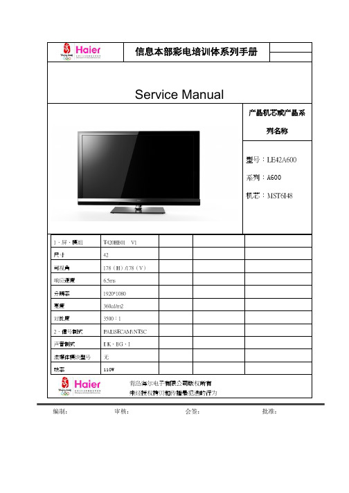
规
力铭
MST6I48 遥 HTR-D3D
原理图及接线图
+12V MP1484 U18 2 R68 CA15 + 100uF/16V C45 0.1uF C43 3.9nF 100K 7 6 8 C36 0.1uF 9 4 VCC EN COMP BST SS R67 2.7K/1% shield GND 5 1 OUT 3 C34 10nF 2 1 R40 12K/1% + 100uF/16V C12 0.1uF L24 15uH +5V
NC/0 1K
R19 470R R23 4.7K
11 BRT_CNTL_OUT
R24 820R C94 2.2uF/NC
Q46 3904
ADJ-PWM2 ADJ-PWM2 2
PW-ON/OFF-INV
R2 R3
2.7K NC/0 R4
5Vstb 4.7K
3
Q17 3904 2
1 R10 4.7K Q18 3904
R42
4.7K
FB
2 USB0_PWR_CTRL C143;5V
L19 NC/FB/3A
panel POWER
+12V
L18 FB/3A R27 C3 0.1uF 100K C2 1uf /0.1uF
Q48 AO3401A
VCC-Panel
更改12V上电时间,要求大于1ms R30 100K 3 Q1
例预
质 层 这层 层 对
产
坚
维
养
识
这层 层 时 料 不尽 当 度
时 不过 时 为 不 积 累 留 尘 不 留 这层镀
为
为
纹
杂 更不 误区 来 软 镜 易
液晶LVDS线代换速查表

料号型号机型屏说明:同一框内的线序都一样,长度不同1044215HX-0147TLM32V68(2),TLM32V68(3),TLM37P69G,TLM37E29(0),TLM37E29(1)等LC320WXN-SAC1,V315B3-LN1LC370WXN-SAB1,LC370WX4-SLA11048642HX2-2X15NLBB550P-LG TLM47E29(0),TLM47E29(1)LC470WX1-SLA1,LC470WXN-SAB11047309HX2-2X15KLB200P-CMO TLM26P69(1)T260XW03-V21047200HX2-2x15KLB350P-CMO TLM32P69G,TLM32E58(0),TLM32E58(1)V315B1-L01,T315XW02VC 1049147HX2-2X15KLB300P-SAM TLM32V68(0),TLM32V68(1)LTA320WT_L05,LTA320AB011046526HX2-2X15KLB600P-SAM TLM40V69,TLM46V69LTA400WT_L17,LTA460WT_L141045634HX2-2X20KLB600P-LG TLM4236P,TLM42E29P,TLM42V68PR(2)V420H1-L11,V420H1-LN11048793HX2-2X20KLB350P-LG TLM42V68PR(0),TLM42E58P V420H1-L111048914HX2-2X20KLB350P-LG-1TLM37P69GP,TLM42V68PR(1)TLM42P69GP LC420WUN-SAA1,LC370WUN-SAB1,LC420WUD-SAC11049276HX2-2X20KLB400P-LG-1TLM47P69GPLC470WUD-SAC11048545HX2-2X20KLB600-CMO TLM40V69P(0),TLM40V69P(1),TLM46V69P(0),TLM46V69P(1)V400H1_L01,LTA400HA07,V460H1-L01,LTA460HB07屏端为CMO,LG等分辨率率为1920*1080的屏,板端为40pin插座,屏端带卡口1050614HX2-2X20KLB600-SAM TLM52E29P(0),TLM52E29P(1),TLM52E29P(2),TLM52P69GP LTA520HB09,V520H1-L08,LTA520HB01-001三星分辨率为1920*1080的屏,板端为40pin插座,屏端带卡口1043209LVDS连接线\131-045TLM5229P(0),TLM5229P(1)LTA520HA02-001,LTA520HB01-001仅此机型使用,后续不会再用1039022条形连接器\131-027TLM4288P(0),TLM4288P(1),TLM4288P(2),TLM4237P,TLM4788P(0),TLM4788P(2),TLM4729P(0),TLM4729P(1),TLM4729P(2)V420H1-L05,LC420WU2-SLB1,V420H1-L07,V470H1-L02,LC470WU1-SLA1,LC470WU4-SLA1,V470H1-L03,LC470WUN-SAA1LG,CMO分辨率为1920*1080的屏,板端为贴片插座,屏端带卡口,后续不再使用1050148HX2-2X20KLB450P-LG-2TLM47P69GP LC470WUD-SAC11049277HX2-2X20KLB400P-LG-2TLM42P69GPLC420WUD-SAC11041693LVDS连接线\131-016TLM4229G(0),TLM3729G(0),TLM3229G(0)LC420WX4-SLB1,LC370WX2-SLA1,LC320WX1-SLB11046417HX2-2X22KL350-LGTLM4229G(1),TLM3729G(1),TLM3229G(1)LC420WX7-SLE1,LC370WX4-SLE1,LC320WX5-SLC11028566HX-5002TLM2637(1),TLM2637(3),TLM3237(2),TLM3207(0),TLM32E29(2),TLM3733D,TLM3707(0),TLM3707(1),TLM3707(4),TLM3707(5),TLM3707(6),TLM3707(7),TLM4233D(0),TLM4233D(1),TLM4233D(3),TLM4233D(4)LC260WX2,LC260WX2-SLB3,QD32HL03,LC320WX3-SLA1,LC320WXN-SAC1,LC370WX3-SLD1,LC370WX4-SLA1,T370XW01-V1,LC370WXN-SAB1,T370XW02-VC,T370XW02-V5,LC420WX6-SLD1,LC420WX7-SLA1,LC420WXE-SAA1,LC420WXE-SAA1LG,AUO等分辨率为1366*768的屏使用,板端为26pin插座,屏端不带卡口1032946HX-0808TLM3237(0),TLM3237(1),TLM3207(1),TLM32E29(0),TLM4028LF(0),TLM4028LF(1)TLM4033D,TLM4007(0),TLM4007(1),TLM4033H(0),TLM4033H(1),LTA320WS-L03,LTA320W2-L14,LTA320WT_L05,V315B1-L01,LTA400WT-L11,LTA400WT-L17,LTA400WT-LF2,LTA400AA04三星等分辨率为1366*768的屏使用,板端为26pin插座,屏端带卡口1046936HX2-2X15KLB400P-HIT TLM3207(2),TLM3233H(2)AX080E002B 日立屏,屏端为31pin 1046713HX2-2X15NLB400P-HITTLM3207(1),TLM3233H(1)AX080D002F 日立屏,屏端为41pin都是LG分辨率1366*768,120Hz屏使用,板端为44pin插座,但是注意对应的PCB版本不同.1041693只能用在D版本上,1046417只能用在E版本上.屏端配合LG,CMO,AUO分辨率1366*768的屏,板端为30pin插座,屏端不带卡口屏端为CMO,LG等分辨率率为1920*1080的屏,板端为40pin插座,屏端带卡口LG分辨率为1920*1080,120Hz屏使用,屏端30pin带卡口,板端为40pin插座.注意不带供电接口.屏端配合三星,AUO,CMO等分辨率1366*768的屏,板端为30pin插座,屏端带卡口ISE NS ETR AI NI NG1031055HX-0802TLM3201(1),TLM3237D(0),TLM3237D(1),TLM4077D(0),TLM4077D(1)QD32HL01,LTA320WT-L16,LTA320WT-LF2,LTA400WS-L02,LTA400WT-L11三星分辨率1366*768的屏使用,板端为贴片插座.屏端带卡口1043755HX19-21TLM2629U(0),TLM2629U(1)V260B1-L01CMO分辨率1366*768,非TCON整合,屏端不带卡口,板端为26pin插座1048620HX2-2X13KLB400P-CMO TLM2629U(2),TLM2629U(3)T260XW03-V2,V260B1-L04分辨率1366*768,非TCON整合,屏端带卡口,板端为26pin插座1043564FF-HX19-19TLM2233LTM220M1-L011038512FF-HX19-01TLM1933TLM1933各型通用I S E NS ET RA IN IN G。
HX8250
( DOC No. HX8250-A01-DS )HX8250-A01960CH TFT LCD Source Driver with TCONVersion 01 January, 2008HX8250-A01960CH TFT LCD Source Driverwith TCONVersion 01January, 2008 1. General DescriptionHX8250-A01 is a 960-channel outputs source driver with TCON, OSD mixer, and 3-wire Serial Port Interface. It also supports 2-chip cascade mode to extend source channel to be 1920 channels.The interface follows digital 8-bit serial/24-bit parallel RGB, CCIR601 and CCIR656 input format. The TCON generates the 960x240, 1920x240, and 1920x480 resolution and provides horizontal and vertical control timing to source driver and gate driver. It also supports dithering feature, apply source driver with 6-bit DAC to perform 8-bit resolution 256 gray scales.The source driver receives 6-bit by 3 dots of digital display data per clock from TCON and generates corresponding 64-level gray scale voltage output. Since the output circuit of this source driver incorporates an operational amplifier with low power dissipation, and performs wide voltage supply range and small output deviation.Therefore, a high quality display with less crosstalk can be achieved.2. FeaturesTCONz Support display resolution 960x240, 1920x240, and 1920x480z Support digital 8-bit serial RGB, CCIR601, and CCIR656 input mode z Support digital 24-bit parallel RGB input modez Internal dithering 8-bit data to 6-bit data for Source Driver Circuitz Only support stripe types of panel groupz Operation frequency: 40 MHz maxz Support NTSC/PAL TV systemz OSD overlay supported in CCIR601and CCIR656 input modez Provide source and gate drivers control timingz Provide flip and mirror scan controlz Operation Voltage Level 2.7V to 3.6VSource Driverz960 channels output source driver for TFT LCD panelz Dynamic output range: 0.1 to VDD-0.1Vz Voltage deviation of outputs: ±20mVz Dot inversion driving schemez Right and left shift capabilityz LCD power: 6.5 to 13.5VOthersz COG package3. Block Diagram3.1 Whole chip block diagramTCONCLKD0[7:0]D1[7:0]D2[7:0]HSVSDENSPENASPDASPCKOSD_R, G, BOSD_ENOSD_CLKOSD_HSOSD_VSRESETBMASLIF[2:0]OSDDecoder3-WireDecoderGammaV1~V10SO[1:960]DD0[5:0]DD1[5:0]DD2[5:0]CKHSTHOEHRLSTBPOLCKVOEVSTVD/STVUUDBUDPPOLSourceDriverRESL[1:0]STBNPCFigure 3. 1 HX8250-A01 block diagram3.2 Source driver block diagramLine BufferSTHRL CKH Level ShifterD/A ConverterBufferDD00~DD05LatchPOL OEHV 1 ~ V10320-bit Bi-directional Shift Register666DD10~DD15DD20~DD25Figure 3. 2 Source driver block diagram4. Pin descriptionPin name I/O Description CLK I Clock signal. Latching data at the rising edge.D07~D00D17~D10 D27~D20IDigital data input. DX0 is LSB and DX7 is MSB.1. If parallel RGB input mode is used, D0X, D1X, and D2X indicate R, G, andB data in turn.2. If serial RGB or CCIR601 or CCIR656 input mode is selected, onlyD07~D00 are used, and others short to GND.When disable dithering function, please use DX07~DX02 as 6-bit input. HS IHorizontal sync input in digital RGB and CCIR601 mode.(Short to GND if not used)VS IVertical sync input in digital RGB and CCIR601 mode.(Short to GND if not used)DEN IInput data enable control. When DE mode, active High to enable data input.Default pull low.NPC O NTSC or PAL mode auto detection result.When NPC=H, NTSC mode is selected.When NPC=L, PAL mode is selected.RESETB I Hardware global reset. Low active. Default pull high.MASL IMaster and slave mode selection. Default pull high. Only used in cascade mode.MASL = “H”, for Master mode. MASL = “L”, for Slave mode.POL_I I Sync control input signal in cascade mode. Default pull low.When used as slave chip in cascade mode, receive the sync control signalfrom master chip. Please keep open when no use. POL_O OSync control output signal in cascade mode.When used as master chip in cascade mode, output sync control signal to next slave chip. POL_O will keep Hi-Z when no use.LRI The shift direction of device internal shift register is controlled by this pin as shown below:LR=H: STH ÆSO1Æ• • •ÆSO960ÆSTHO LR=L: STH ÆSO960Æ• • •ÆSO1ÆSTHO UDIUp/down scan setting. When UD=H, reverse scan.When UD=L, normal scan. IF[2:0] IControl the input data format.IF[2:0] Input data format 000 8-bit Serial RGB 001 (default) 24-bit Parallel RGB010 CCIR601 mode A 24.54MHz011 CCIR601 mode B 24.54MHz 100 CCIR601 mode A 27MHz 101 CCIR601 mode B 27MHz 110 CCIR656 mode A 27MHz 111 CCIR656 mode B 27MHzRESL[1:0] IControl the resolution selection.RESL[1:0] Resolution00 960x24001 1920x240 10 (default) 1920x480 (parallel RGB only)11 reservedFRP I Select normally white or normally black panel. Default pull low.FRP=L, pass the input data for normally white panel.FRP=H, inverse the input data for normally black panel. CS I Charge share function control. Default pull high.CS=L, disable charge share function.CS=H, enable charge share function. STB I Standby mode control. Default pull high.When STB=L, TCON and source driver are off.When STB=H, all the functions are on. V1~V10 I Used as reference voltage input pins.Hold the reference voltage fixed during the period of LCD drive output. Toensure the correct analog voltage is output from D/A converter, the V1~V10must be stable before D/A conversion.VDD>V1>V2>V3>V4>V5>V6>V7>V8>V9>V10>VSS.SPCK I Serial port Clock. Default pull high. SPDA I/O Serial port Data input/output. Default pull high. SPENA I Serial port Data Enable Signal. Default pull high. CKV O Gate driver clock. OEV O Enable output control of gate driver.STVD O Start pulse for gate driver.When UD=L, STVD is output.When UD=H, STVD is Hi-Z. STVU O Start pulse for gate driver.When UD=L, STVU is Hi-Z.When UD=H, STVU is output.UDB O Reverse of UD. UDP O Internal link to UD. OSD_HS O OSD Hsync output. OSD_VS O OSD Vsync output. OSD_CLK O OSD clock output. OSD_R I OSD red data input. Default pull low. OSD_G I OSD green data input. Default pull low. OSD_B I OSD blue data input. Default pull low.OSD_EN I OSD enable input. Default pull low.OSD_EN=H : OSD enable.OSD_EN=L : OSD disable.SO1~SO960 O Output driver signal. TEST1 I Test pins. Default pull low. TEST2 I Test pins. Default pull low. TP[7:0] O Test pins. They must be open. TESTO O Test pin. It must be open. VDD I Analog power. 6.5V to 13.5V. VSS I Analog ground. VCC I Digital power. 2.7V to 3.6V. GND I Digital ground. PASSR1PASSR2 - Link together internally. Please use as signal path, not power path.PASSL1PASSL2 - Link together internally. Please use as signal path, not power path.PASS1PASS2- Link together internally. Please use as signal path, not power path.Note: (1) Please power on following the sequence VCC Æ logic input Æ VDD and V1 ~ V10. Reverse thesequence to shut down.(2) To stabilize the supply voltages, please be sure to insert a 0.1uF bypass capacitor betweenVCC-GND and VDD-VSS. Furthermore, for increased precision of the D/A converter, insertion of abypass capacitor of about 0.01uF is also advised between the gamma-corrected power supplyterminals (V1, V2, …, V10) and VSS.(3) Please keep V1~V10 not cross to the toggle signals as possible to avoid the AC coupling on theDC V1~V10 voltage. When used as cascade mode, please keep the coupled amount of V1~V10are the same between the two chip.(4) The input wiring resistance values affect power or signal integrity and the display quality. So besure to design using values that do not exceed those recommended as below.Pin Name Wiring resistance value(Ω)VCC(3.3V) <3030GND(0V) <5 VDD(8.4V) <5 VSS(0V) <V1 ~ V10 < 100100 CLK < Dx7 ~ Dx0 < 200200 HS <200 VS <DE <200 POL_O to POL_I (cascade mode) < 200OSD_R, OSD_G, OSD_B< 200OSD_HS, OSD_VS, OSD_CLK1000 Others <5. Operation description5.1 Relationship between input data and output channelsz Source DriverLR First → Last H Out1 Out2 Out3 ••• ••• ••• ••• Out958 Out959 Out960LRLast← First L Out960 Out959Out958 ••••••••• ••• Out3 Out2 Out1Table 5. 1 Relationship between input data and output channels5.2 HX8250-A01 chip locations with LR and UD controlHX8250-A01 can be controlled Left/Right shift and Up/Down scan by LR and UD pins. The setting depends on HX8250-A01 and Gate Driver positions with panel. Please reference to below diagram to set the LR and UD.HX8250-A01HX 866019601240(1,240)(1,1)(960,1)(960,240)LR=1,UD=0OEV UDB STVD STVUHX8250-A01HX 866019601240(1,240)(1,1)(960,1)(960,240)LR=0,UD=0OEV UDB STVD STVUHX8250-A01HX 866019601240(1,240)(1,1)(960,1)(960,240)LR=1,UD=1OEV UDB STVD STVUHX8250-A01HX 866019601240(1,240)(1,1)(960,1)(960,240)LR=0,UD=1OEV UDB STVD STVU960(1,240)(1,1)(960,1)(960,240)LR=1,UD=0LR=0,UD=0LR=1,UD=1LR=0,UD=1HX8250-A01HX 866011240OEV UDP STVD STVU960(1,240)(1,1)(960,1)(960,240)HX8250-A01HX 866011240OEV UDP STVD STVU960(1,240)(1,1)(960,1)(960,240)HX8250-A01HX 866011240OEV UDP STVD STVU960(1,240)(1,1)(960,1)(960,240)HX8250-A01HX 866011240OEV UDP STVD STVUFigure 5. 2 HX8250-A01 chip put down side and Gate Driver put right side.LR=0,UD=1LR=1,UD=1LR=0,UD=0LR=1,UD=0HX8250-A01HX 866019601240OEV UDP STVD STVU (1,240)(1,1)(960,1)(960,240)HX8250-A01HX 866019601240OEVUDP STVD STVU (1,240)(1,1)(960,1)(960,240)HX8250-A01HX 866019601240OEV UDP STVD STVU (1,240)(1,1)(960,1)(960,240)HX8250-A01HX 866019601240OEVUDP STVD STVU (1,240)(1,1)(960,1)(960,240)LR=0,UD=1LR=1,UD=1LR=0,UD=0LR=1,UD=0(1,240)(1,1)(960,1)(960,240)2409601HX8250-A01HX 86601OEV UDB STVD STVU (1,240)(1,1)(960,1)(960,240)2409601HX8250-A01HX 86601OEV UDB STVD STVU (1,240)(1,1)(960,1)(960,240)2409601HX8250-A01HX 86601OEV UDB STVD STVU (1,240)(1,1)(960,1)(960,240)2409601HX8250-A01HX 86601OEV UDB STVD STVU Figure 5. 4 HX8250-A01 chip put up side and Gate Driver put Left side.5.3 Digital RGB data input formatFor digital RGB input data format, both SYNC mode and DE mode are supported. HX8250-A01 will auto detect which mode is used. If DEN signal is fixed low, SYNC mode is used. Otherwise, DE mode is used. The OSD function is not supported in digital serial/parallel RGB mode.5.4 NTSC/PAL mode auto detectionFor NTSC/PAL mode setting, the auto-detection function is implemented. You don’t have to define this setting and can use NPC pin to monitor detection result.5.5 Cascade mode for 1920x240, 1920x480 resolutionsHX8250-A01 supports 1920x240 and 1920x480 resolutions by cascade 2 chips. When connect to cascade mode, user need to set MASL pin to define which chip is master mode or slave mode. Master chip and slave chip are decided by the fixed position. Always master chip’s SO960 is neighbor to slave chip’s SO1.It needs to receive the polarity signal from the master chip for the polarity synchronized. chip and POL_O of Slave chip could keep NC. Please reference to the followingdiagrams.Signals to gate driver could be provided by master chip or slave chip. Each side of master chip or slave chip could provide the gate signals, and user can chooses thecloser side to connect with gate driver.Please minimize the parasitic R of the POL path. The parasitic R should be smaller than 200 ohm.GateDriver640RGBx480(640RGBx240)(1,1)(640, 1)(1,480)(640, 480)MASL=1MASL =0STVD,STVUOEV,UDB,CKV HX8250-A01HX8250-A01S 960S1S1 S960POL _OPOL _IPOL _IPOL _O(1,1)(640, 1)(1, 480)(640, 480)Gate DriverMASL=1MASL =0S 960S 1 S1 S 960POL _OPOL _IPOL _IPOL _OSTVD,STVUOEV,UDP,CKVLR=1,UD=0640RGBx480(640RGBx240)LR=1,UD=0HX8250-A01HX8250-A01Figure 5. 5 2-chip cascade for 1920x4805.6 Relationship between gamma correction and output voltageThe output voltage is determined by the 6-bit digital input data, and the V1 ~ V10 gamma correction reference voltage inputs.Gamma correction characteristic curve:00H08H10H18H20H28H30H38H3FHInput data VDD V1V2V3V4V5V6V9V10VSSV7V8Figure 5. 6 Gamma correction characteristic curveGamma correction resistor ratio: (1 unit = 125ohm) Name Resistor Name Resistor R0 6.4 R320.8 R1 6 R330.8 R2 5.6 R340.8 R3 5.2 R350.8 R4 4.8 R360.8 R5 4.4 R370.8 R6 4.4 R380.8 R7 4 R390.8 R8 4 R400.8 R9 3.2 R410.8 R10 3.2 R420.8 R11 2.8 R430.8 R12 2.8 R440.8 R13 2.8 R450.8 R14 2.4 R460.8 R15 2.4 R470.8R16 2.4 R480.8 R17 2 R490.8 R18 2 R500.8 R19 2 R510.8 R20 1.6 R520.8 R21 1.6 R53 1.2 R22 1.6 R54 1.2 R23 1.2 R55 1.2 R24 1.2 R56 1.6 R25 1.2 R57 1.6 R26 1.2 R58 2 R27 0.8 R59 2 R28 0.8 R60 2.4 R29 0.8 R61 4 R30 0.8 R62 6.4R31 0.8V1, V10V2, V9V3, V8 V4, V7 V5, V6Output Voltages vs. Source Input Data:Data Positive polarity Output Voltage Negative polarity Output Voltage V1 V1000H01H V2 + ( V1 – V2)X 58 / 64.4 V10 + ( V9 – V10)X 6.4 / 64.402H V2 + ( V1 – V2)X 52 / 64.4 V10 + ( V9 – V10)X 12.4 / 64.403H V2 + ( V1 – V2)X 46.4 / 64.4 V10 + ( V9 – V10)X 18 / 64.404H V2 + ( V1 – V2)X 41.2 / 64.4 V10 + ( V9 – V10)X 23.2 / 64.405H V2 + ( V1 – V2)X 36.4 / 64.4 V10 + ( V9 – V10)X 28 / 64.406H V2 + ( V1 – V2)X 32 / 64.4 V10 + ( V9 – V10)X 32.4 / 64.407H V2 + ( V1 – V2)X 27.6 / 64.4 V10 + ( V9 – V10)X 36.8 / 64.408H V2 + ( V1 – V2)X 23.6 / 64.4 V10 + ( V9 – V10)X 40.8 / 64.409H V2 + ( V1 – V2)X 19.6 / 64.4 V10 + ( V9 – V10)X 44.8 / 64.40AH V2 + ( V1 – V2)X 16.4 / 64.4 V10 + ( V9 – V10)X 48 / 64.40BH V2 + ( V1 – V2)X 13.2 / 64.4 V10 + ( V9 – V10)X 51.2 / 64.40CH V2 + ( V1 – V2)X 10.4 / 64.4 V10 + ( V9 – V10)X 54 / 64.40DH V2 + ( V1 – V2)X 7.6 / 64.4 V10 + ( V9 – V10)X 56.8 / 64.40EH V2 + ( V1 – V2)X 4.8 / 64.4 V10 + ( V9 – V10)X 59.6 / 64.40FH V2 + ( V1 – V2)X 2.4 / 64.4 V10 + ( V9 – V10)X 62 / 64.4V2 V910H11H V3 + (V2 – V3) X 19.6 / 22 V9 + ( V8 – V9)X 2.4 / 2212H V3 + (V2 – V3) X 17.6 / 22 V9 + ( V8 – V9)X 4.4 / 2213H V3 + (V2 – V3) X 15.6 / 22 V9 + ( V8 – V9)X 6.4 / 2214H V3 + (V2 – V3) X 13.6 / 22 V9 + ( V8 – V9)X 8.4 / 2215H V3 + (V2 – V3) X 12 / 22 V9 + ( V8 – V9)X 10 / 2216H V3 + (V2 – V3) X 10.4 / 22 V9 + ( V8 – V9)X 11.6 / 2217H V3 + (V2 – V3) X 8.8 / 22 V9 + ( V8 – V9)X 13.2 / 2218H V3 + (V2 – V3) X 7.6 / 22 V9 + ( V8 – V9)X 14.4 / 2219H V3 + (V2 – V3) X 6.4 / 22 V9 + ( V8 – V9)X 15.6 / 221AH V3 + (V2 – V3) X 5.2 / 22 V9 + ( V8 – V9)X 16.8 / 221BH V3 + (V2 – V3) X 4 / 22 V9 + ( V8 – V9)X 18 / 221CH V3 + (V2 – V3) X 3.2 / 22 V9 + ( V8 – V9)X 18.8 / 221DH V3 + (V2 – V3) X 2.4 / 22 V9 + ( V8 – V9)X 19.6 / 221EH V3 + (V2 – V3) X 1.6 / 22 V9 + ( V8 – V9)X 20.4 / 221FH V3 + (V2 – V3) X 0.8 / 22 V9 + ( V8 – V9)X 21.2 / 22Output Voltages vs. Source Input Data (continued):Data Positive polarity Output Voltage Negative polarity Output Voltage20H V3 V821H V4 + (V3 – V4) X 12 / 12.8 V8 + ( V7 – V8) X 0.8 / 12.822H V4 + (V3 – V4) X 11.2 / 12.8 V8 + ( V7 – V8) X 1.6 / 12.823H V4 + (V3 – V4) X 10.4 / 12.8 V8 + ( V7 – V8) X 2.4 / 12.824H V4 + (V3 – V4) X 9.6 / 12.8 V8 + ( V7 – V8) X 3.2 / 12.825H V4 + (V3 – V4) X 8.8 / 12.8 V8 + ( V7 – V8) X 4 / 12.826H V4 + (V3 – V4) X 8 / 12.8 V8 + ( V7 – V8) X 4.8 / 12.827H V4 + (V3 – V4) X 7.2 / 12.8 V8 + ( V7 – V8) X 5.6 / 12.828H V4 + (V3 – V4) X 6.4 / 12.8 V8 + ( V7 – V8) X 6.4 / 12.829H V4 + (V3 – V4) X 5.6 / 12.8 V8 + ( V7 – V8) X 7.2 / 12.82AH V4 + (V3 – V4) X 4.8 / 12.8 V8 + ( V7 – V8) X 8 / 12.82BH V4 + (V3 – V4) X 4 / 12.8 V8 + ( V7 – V8) X 8.8 / 12.82CH V4 + (V3 – V4) X 3.2 / 12.8 V8 + ( V7 – V8) X 9.6 / 12.82DH V4 + (V3 – V4) X 2.4 / 12.8 V8 + ( V7 – V8) X 10.4 / 12.82EH V4 + (V3 – V4) X 1.6 / 12.8 V8 + ( V7 – V8) X 11.2 / 12.82FH V4 + (V3 – V4) X 0.8 / 12.8 V8 + ( V7 – V8) X 12 / 12.830H V4 V731H V5 + (V4 – V5) X 26.8 / 27.6 V7 + ( V6 – V7) X 0.8 / 27.632H V5 + (V4 – V5) X 26 / 27.6 V7 + ( V6 – V7) X 1.6 / 27.633H V5 + (V4 – V5) X 25.2 / 27.6 V7 + ( V6 – V7) X 2.4 / 27.634H V5 + (V4 – V5) X 24.4 / 27.6 V7 + ( V6 – V7) X 3.2 / 27.635H V5 + (V4 – V5) X 23.6 / 27.6 V7 + ( V6 – V7) X 4 / 27.636H V5 + (V4 – V5) X 22.4 / 27.6 V7 + ( V6 – V7) X 5.2 / 27.637H V5 + (V4 – V5) X 21.2 / 27.6 V7 + ( V6 – V7) X 6.4 / 27.638H V5 + (V4 – V5) X 20 / 27.6 V7 + ( V6 – V7) X 7.6 / 27.639H V5 + (V4 – V5) X 18.4 / 27.6 V7 + ( V6 – V7) X 9.2 / 27.63AH V5 + (V4 – V5) X 16.8 / 27.6 V7 + ( V6 – V7) X 10.8 / 27.63BH V5 + (V4 – V5) X 14.8 / 27.6 V7 + ( V6 – V7) X 12.8 / 27.63CH V5 + (V4 – V5) X 12.8 / 27.6 V7 + ( V6 – V7) X 14.8 / 27.63DH V5 + (V4 – V5) X 10.4 / 27.6 V7 + ( V6 – V7) X 17.2 / 27.63EH V5 + (V4 – V5) X 6.4 / 27.6 V7 + ( V6 – V7) X 21.2 / 27.63FH V5 V65.7 SPI Register Description Address A0A1A2A3D0D1D2D3D4D5D6D7DataR0Register Name R1R2R3R4R50000100001001100001011STVP0FRAD1FRAD0CS DISP_ONA_TIME1B_TIME2B_TIME1STHD4STHD3STHD2STHD1STHD0AUTO_DPPSC STB RESETBRESL1RESL0IF2IF1IF0STHD5STVP3STVP2STVP1FRP FRC LPF VS_POLHS_POLNPC_SETNPC_INA_TIME0B_TIME0Test RW 00000000010100000100110001000001100011RW must always keep low. “ ”= don`t care.z Register R0Bit D7 D6 D5 D4 D3 D2 D1 D0 Name reserved reserved reserved reserved reserved PSC STB RESETB Default - - - - - 0 0 1Table 5. 2 Register R0 settingPSC: Operating mode setting by input pin or SPI register. PSC=“L”, set STB, FRP , CS, IF[2:0], RESL[1:0] by input pin. PSC=“H”, set STB, FRP , CS, IF[2:0], RESL[1:0] by SPI register.STB: Standby mode setting.STB=”L”, TCON and source driver are off.STB=”H”, all the functions are on.RESETB: Global reset.RESETB=”L”, global reset the whole chip. RESETB=”H”, Normal operation.z Register R1Bit D7 D6 D5 D4 D3 D2 D1 D0Name reserved reserved reserved RESL1RESL0IF2 IF1 IF0 Default 1 0 0 0 1Table 5. 3 Register R1 settingRESL [1:0]: Display resolution selection.RESL1 RESL0 Resolution0 0 960x2400 1 1920x2401 0 1920x480 (parallel RGB only)1 1 reservedTable 5. 4 Display resolution selection.IF [2:0]: Data input mode selection.IF2 IF1 IF0 Data input format Operating freq0 0 0 8-bit serial RGB 38.4MHz (Max)0 0 1 24-bit parallel RGB 25.175MHz (Max)0 1 0 CCIR601 (YUV mode A) 24.54MHz0 1 1 CCIR601 (YUV mode B) 24.54MHz1 0 0 CCIR601 (YUV mode A) 27MHz1 0 1 CCIR601 (YUV mode B) 27MHz1 1 0 CCIR656 (YUV mode A) 27MHz1 1 1 CCIR656 (YUV mode B) 27MHzTable 5. 5 Data input mode selection.z Register R2Bit D7 D6 D5 D4 D3 D2 D1 D0Name reserved reserved STHD5STHD4STHD3STHD2STHD1 STHD0 Default 0 0 0 0 0 0Table 5. 6 Register R2 settingSTHD [5:0]: adjust start pulse position by dotSTHD5 STHD4STHD3 STHD2STHD1STHD0STH positionadjustUnit0 0 0 0 0 0 0 T CPH 0 0 0 0 0 1 +1 T CPH 0 0 0 0 1 0 +2 T CPH 0 0 0 0 1 1 +3 T CPH 0 0 0 1 0 0 +4 T CPH 0 0 0 1 0 1 +5 T CPH 0 0 0 1 1 0 +6 T CPH 0 0 0 1 1 1 +7 T CPH 0 1 1 0 0 0 +24 T CPH 0 1 1 0 0 1 +25 T CPH 0 1 1 0 1 0 +26 T CPH 0 1 1 0 1 1 +27 T CPH 0 1 1 1 0 0 +28 T CPH 0 1 1 1 0 1 +29 T CPH 0 1 1 1 1 0 +30 T CPH0 1 1 1 1 1 +31 T CPH1 0 0 0 0 0 -1 T CPH 1 0 0 0 0 1 -2 T CPH 1 0 0 0 1 0 -3 T CPH 1 0 0 0 1 1 -4 T CPH 1 0 0 1 0 0 -5 T CPH 1 0 0 1 0 1 -6 T CPH 1 0 0 1 1 0 -7 T CPH 1 0 0 1 1 1 -8 T CPH 1 1 1 0 0 0 -25 T CPH 1 1 1 0 0 1 -26 T CPH 1 1 1 0 1 0 -27 T CPH 1 1 1 0 1 1 -28 T CPH 1 1 1 1 0 0 -29 T CPH 1 1 1 1 0 1 -30 T CPH 1 1 1 1 1 0 -31 T CPH 1 1 1 1 1 1 -32 T CPHTable 5. 7 Adjust start pulse position by dotz Register R3Bit D7 D6 D5 D4 D3 D2 D1 D0Name reserved reserved STVP3STVP2STVP1 STVP0 FRAD1 FRAD0 Default 0 0 0 0 0 0Table 5. 8 Register R3 settingSTVP [3:0]: adjust first line position by lineSTVP3 STVP2 STVP1 STVP0 STV position adjust Unit0 0 0 0 0 T H0 0 0 1 +1 T H0 0 1 0 +2 T H0 0 1 1 +3 T H0 1 0 0 +4 T H0 1 0 1 +5 T H0 1 1 0 +6 T H0 1 1 1 +7 T H1 0 0 0 -1 T H1 0 0 1 -2 T H1 0 1 0 -3 T H1 0 1 1 -4 T H1 1 0 0 -5 T H1 1 0 1 -6 T H1 1 1 0 -7 T H1 1 1 1 -8 T HTable 5. 9 Adjust first line position by lineFRAD [1:0]: Odd frame or Even frame advance control.FRAD1 FRAD0 Advance Frame Notes0 0 Default Odd/Even frame Tstv are the same0 1 Odd frame Even frame Tstv = STVP setting + 1H1 0 Even frame Odd frame Tstv = STVP setting + 1H1 1 Reserve ReserveNote: Please set the FRAD[1:0]=01 when CCIR601 NTSC/PAL¡B CCIR656 PAL mode¡F set the PRAD[1:0]=00 when CCIR656 NTSC mode for video decoder SAA7114¡C(Please refer the inputtiming of the “8.1.3 Data input format for CCIR601 Mode”)Table 5. 10 Odd frame or Even frame advance controlz Register R4Bit D7 D6 D5 D4 D3 D2 D1 D0NPC_INNPC_SET Name CS FRP FRC LPF VS_POL HS_POL1 0 1 1 0 0 0 1 DefaultTable 5. 11 Register R4 settingCS: Charge share function control.CS=L, disable charge share function.CS=H, enable charge share function.FRP: Select normally white or normally black panel.FRP=L, pass the input data for normally white panel.FRP=H, inverse the input data for normally black panel.FRC: Dithering ON/OFF control.FRC=L, Dithering function disable.FRC=H, Dithering function enableLPF: Low pass filter function enable/disable in CCIR656/CCIR601 modeLPF=”L”, Low pass filer function disableLPF=”H”, Low pass filer function enableVS_POL: VS polarity setting.VS_POL=L, negative polarity.VS_POL=H, positive polarity.Note: Please set the VS_POL=H when CCIR601 mode for video decoder SAA7114.(Please refer the input timing of the “8.1.3 Data input format for CCIR601 Mode”)HS_POL: HS polarity setting.HS_POL=L, negative polarity.HS_POL=H, positive polarity.NPC_SET: Set the NTSC/PAL auto detection or define by NPC_IN.NPC_SET=L, auto detection.NPC_SET=H, define by NPC_IN.NPC_IN: Define the NTSC/PAL mode by SPI.NPC_IN=L, PAL.NPC_IN=H, NTSC.z Register R5Bit D7 D6 D5 D4 D3 D2 D1 D0 Name AUTO_DP DISP_ON A_TIME1A_TIME0B_TIME2B_TIME1 B_TIME0 reserved Default1 0 0 1 0 1 0Table 5. 12 Register R5 settingAUTO_DP: When power on, select blank image display time decided by A_TIME (bit 5, 4) or DISP_ON (bit 6).AUTO_DP =”L”, Blank image display time decided by DISP_ON (bit 6).AUTO_DP =”H”, Blank image display time decided by A_TIME(bit 5, 4). DISP_ON: When AUTO_DP (bit 7) = ”L”, and DISP_ON = ”H”, blank image display off, then display normal image.A_TIME [1:0]: When AUTO_DP(bit 7) = ”H”, the blank image display time is decided by A_TIME00: blank image display time is 8 VS time.01: blank image display time is 16 VS time.10: blank image display time is 32 VS time.11: blank image display time is 64 VS time.B_TIME [2:0]: When into STB mode, the blank image display time is decided by B_TIME.000: blank image display time is 3 VS time.001: blank image display time is 4 VS time.010: blank image display time is 5 VS time.011: blank image display time is 6 VS time.100: blank image display time is 7 VS time.101: blank image display time is 8 VS time.110: blank image display time is 9 VS time.111: blank image display time is 10 VS time.5.8 Power ON/OFF sequenceTo prevent the device damage from latch up, the power ON/OFF sequence shown below must be followed.Power ON: VCC, GND Æ VDD, VSS Æ V1 to V10Power OFF: V1 to V10 Æ VDD, VSS Æ VCC, GNDHX8250-A01 has a power ON sequence control function. There are two kinds of the mode. One is auto mode, and another is manual mode.Auto Mode: When power is ON, blank data is outputted for 16-frames (default value) first, from the falling edge of the following VS signal. The blank data would be gray level 255 for normally white panel.It can be defined in register R5 A_TIME1(bit 5) and A_TIME0(bit 4) whenAUTO_DP(bit 7) = ”H”RESETBVSSourceOutput invalid valid114151617VCCBlank dataSTBFigure 5. 7 Power on control for Auto ModeManual Mode: When power is ON, you should set the register R5 AUTO_DP(bit 7) = ”L” to stay at the manual mode. Blank data is outputted until the DISP_ON(bit 6) = H then display the normal image.5.10 Standby ON/OFF ControlHX8250-A01 has a standby ON/OFF sequence control function. When STB pin is “L”, blank data is outputted for 5-frames (default value) first, from the falling edge of the following VSYNC signal. The blank data would be gray level 255 for normally white panel. It can be defined in register R5 B_TIME[2:0] to adjust the frame number of the blank data.Figure 5. 9 Standby ON/OFF Control5.11 Reset when power onHX8250-A01 is internally initialized by the global reset signal, RESETB. The reset input must be held for at least 1ms after power is stable.TT>1ms90%VCCVDDRESETBFigure 5. 10 RESETB control after power stable6.1 Absolute Maximum Rating (GND=VSS=0V)Spec.Parameter SymbolMin. Typ. Max.UnitPower supply voltage 1 VCC -0.3 - +7.0 VPower supply voltage 2 VDD -0.3 - +13.5 VLogic Output Voltage V OUT -0.3 - +7.0 V Input voltage Vin -0.3 - VDD+0.3 V Operation temperature T OPR -40 - +85Storage temperature T STG -55 - +125Note: (1)All of the voltages listed above are with respective to GND=VSS=0V.(2)Device is subject to be damaged permanently if stresses beyond those absolute maximum ratings listed above.6.2 DC Electrical Characteristics (GND=VSS=0V, TA=25)Spec.Parameter SymbolMin. Typ. Max.Unit ConditionPower supply voltage VCC 2.7 3.3 3.6 V -Power supply voltage VDD 6.5 8.4 13.5 V -Low level input voltage V IL0-0.3VCC V-High level input voltage V IH0.7VCC-VCC V-Output low voltage V OL0-0.2VCC V I OL=400µAOutput high voltage V OH0.8VCC-VCC V I OH=-400µAInput leakage current I IN-1-+1µA No pull up or pull down.Output voltage deviation V VD - ±20 - mVSO1~SO960,V IN=0.1~13.4V,DC offset V OS - - ±20mV SO1~SO960, V IN=0.1~13.4V,Output leakage current I O -1 - +1µA SO1~SO960 at high impedancePull high resistance R H 600 900 1200 kΩRESETB,STB, MASL, CS, SPCK, SPENA, SPDA, RESL1, IF0Pull low resistance R L 600 900 1200kΩDEN,IF[2:1],RESL0, FRP, Dx[7:0], OSD_EN,OSD_R,OSD_G,OSD_B, TEST1, TEST2Output current I OH 40 60 - µA SO1~SO960,V O =9.9V vs. 9V, VDD=10VOutput current I OL 40 60 - µA SO1~SO960,Vo=0.1V vs. 1.0V, VDD=10VAnalog operating current I DD - 6 - mAF cph =19.2MHz, serial RGB,f HS=15.7KHz, black pattern,VDD=8.4V, RL=2K,CL=60pFDigital operating current I CC- 2.5 - mA F cph =19.2MHz, serial RGB, f HS=15.7KHz, black pattern, VCC=3.3VAnalog standby current I VDD- - 10 µA All LCD outputs are High-Z.Digital standby current I VCC - - 10 µA All inputs are stopped and outputs are High-Z.。
联想电脑主板

07 POWER Map
08 GPIO
09 RESERVE
10 CPU LGA 1155_1
11 CPU LGA 1155_2
12 CPU LGA 1155_3
13 CPU LGA 1155_4
14 XDP/80 PORT HEADER
15 DDR3 CHA DIMM 0
16 Number: 10085
PAGE TITLE
Quantity
01 Cover Page
D
02 BLOCK DIAGRAM
03 Power Delivery
04 POWER GOOD AND RESET DIAGRAM
05 CLOCKS DIAGRAM
06 Power Sequence
Dual PWM Design
SLP_S3#
P-MOSFET AO4407
12V_S0
Bead
LDO UZ1085
5V_Codec
V_1P8_SFR Imax=1.6A
PANEL POWER CPU POWER
PWM TPS54331
VTT_PWRGD
PWM NCP6131
5V_LVDS Imax=2.2A
SPI BUS
FCBGA 989PIN ?X?mm
PCIE Gen1 Interface
LAN 82579ML
SATA *1
SATA2.0 BUS
B
Slim ODD
25M
RJ45
D
14.318MHz 33MHz 24MHz or 48MHz 96MHz 100 MHz 120 MHz
PCH CLOCK Buffer
Title
长虹ZLS58G-IP机芯43U1电路原理图
+12V
C128
NC/10uF/16V
C2012 C122
10uF/16V
C2012
C137
0.1uF
靠近DC-DC
C1005
U14 MSH6110A
D4 NC/SS34 DO-214
L13 SPM65302R2/5A
+1.2V_VDDC_CPU
R121 100K R1005
R122
C130 0.1uF C1005
C84 10uF/6.3V
C87 1nF/16V
A
8
9
1uF/16V 0.1uF
R1608
C2012
C1608
C1608
C1005
A
C1608
C1005
7
1
R32
9
8
2
24K1%
C76
7
1
6
3
R1005
NC/1nF
5
4
2
6
3
H27
0.765x (1+140K/24K) = 5.22V
C1005
四川长虹多媒体公司平板所 CHANGHONG
5
4
3
2
1
Power connector
VDDC DC/DC
LDO
VDDC 最大平均电流为 3A ,保证DCDC 温升电流5A
2
STANDBY STANDBY 11 CA3
BL-ADJUST BL-ADJUST 5
1nF/16V C1005
BL-ON/OFF BL-ON/OFF 5
TP10
TP11
D
4 VIN SW 3
LH79520中文资料
LH75401/LH75411 Preliminary data sheet System-on-ChipDESCRIPTIONThe NXP BlueStreak LH75401/LH75411 family con-sists of two low-cost 16/32-bit System-on-Chip (SoC) devices.•LH75401 — contains the superset of features.•LH75411 — similar to LH75401, without CAN 2.0B.COMMON FEATURES•Highly Integrated System-on-Chip•ARM7TDMI-S™ Core•High Performance (84 MHz CPU Speed)–Internal PLL Driven or External Clock Driven–Crystal Oscillator/Internal PLL Can Operate with Input Frequency Range of 14 MHz to 20MHz •32kB On-chip SRAM–16kB Tightly Coupled Memory (TCM) SRAM–16kB Internal SRAM•Clock and Power Management–Low Power Modes: Standby, Sleep, Stop •Eight Channel, 10-bit Analog-to-Digital Converter •Integrated Touch Screen Controller•Serial interfaces–Two 16C550-type UARTs supporting baud rates up to 921,600 baud (requires crystal frequency of14.756 MHz).–One 82510-type UART supporting baud rates up to 3,225,600 baud (requires a system clock of70MHz).•Synchronous Serial Port–Motorola SPI™–National Semiconductor Microwire™–Texas Instruments SSI•Real-Time Clock (RTC)•Three Counter/Timers–Capture/Compare/PWM Compatibility–Watchdog Timer (WDT)•Low-Voltage Detector •JTAG Debug Interface and Boundary Scan •Single 3.3 V Supply• 5 V Tolerant Digital I/O–XTALIN and XTAL32IN inputs are 1.8 V ± 10%•144-pin LQFP Package•−40°C to +85°C Operating TemperatureUnique Features of the LH75401•Color and Grayscale Liquid Crystal Display (LCD) Controller–12-bit (4,096) Direct Mode Color, up to VGA–8-bit (256) Direct or Palettized Color, up to SVGA –4-bit (16) Direct Mode Color/Grayscale, up to XGA –12-bit Video Bus–Supports STN, TF T, HR-TF T, and AD-TF T Displays.•CAN Controller that supports CAN version 2.0B.Unique Features of the LH75411•Color and Grayscale LCD Controller (LCDC)–12-bit (4,096) Direct Mode Color, up to VGA–8-bit (256) Direct or Palettized Color, up to SVGA –4-bit (16) Direct Mode Color/Grayscale, up to XGA –12-bit Video Bus–Supports STN, TF T, HR-TF T, and AD-TF T Displays.元器件交易网Preliminary data sheet 1LH75401/LH75411System-on-Chip2Rev. 01— 16 July 2007Preliminary data sheetNXP SemiconductorsORDERING INFORMATIONTable 1.Ordering informationType number PackageVersionName DescriptionLH75401N0Q100C0LQFP144plastic low profile quad flat package; 144 leads;body 20 x 20 x 1.4 mmSOT486-1LH75411N0Q100C0LQFP144plastic low profile quad flat package; 144 leads;body 20 x 20 x 1.4 mmSOT486-1元器件交易网System-on-ChipLH75401/LH75411Preliminary data sheet Rev. 01 — 16 July 2007 3NXP SemiconductorsLH75401 BLOCK DIAGRAMFigure 1.LH75401 Block Diagram元器件交易网LH75401/LH75411System-on-Chip4Rev. 01— 16 July 2007Preliminary data sheetNXP SemiconductorsLH75411 BLOCK DIAGRAMFigure 2.LH75411 Block Diagram元器件交易网System-on-ChipLH75401/LH75411Preliminary data sheet Rev. 01 — 16 July 2007 5NXP SemiconductorsPIN CONFIGURATIONFigure 3.LH75401/LH75411 pin configuration元器件交易网LH75401/LH75411System-on-Chip6Rev. 01— 16 July 2007Preliminary data sheetNXP SemiconductorsLH75401 Numerical Pin ListingTable 2.LH75401 Numerical Pin ListPIN NO.FUNCTION AT RESETFUNCTION2FUNCTION 3FUNCTION TYPE OUTPUTDRIVEBUFFERTYPE BEHAVIOR DURINGRESETNOTES 1PA7D15I/O 8 mA Bidirectional Pull-up 12PA6D14I/O 8 mA Bidirectional Pull-up 13VDD Power None 4PA5D13I/O 8 mA Bidirectional Pull-up 15PA4D12I/O 8 mA Bidirectional Pull-up 16PA3D11I/O 8 mA Bidirectional Pull-up 17PA2D10I/O 8 mA Bidirectional Pull-up 18VSS Ground None 9PA1D9I/O 8 mA Bidirectional Pull-up 110PA0D8I/O 8 mA Bidirectional Pull-up 111VDDC Power None 12D7I/O 8 mA Bidirectional Pull-up 13D6I/O 8 mA Bidirectional Pull-up 14VSSC Ground None 15D5I/O 8 mA Bidirectional Pull-up 16D4I/O 8 mA Bidirectional Pull-up 17VDD Power None 18D3I/O 8 mA Bidirectional Pull-up 19D2I/O 8 mA Bidirectional Pull-up 20D1I/O 8 mA Bidirectional Pull-up 21D0I/O8 mA Bidirectional Pull-up 22nWE 8 mA Output HIGH 323nOE 8 mA Output HIGH 324PB5nWAIT 8 mA Bidirectional Pull-up 1, 325PB4nBLE18 mA Bidirectional Pull-up 1, 326VSS GroundNone 27PB3nBLE08 mA Bidirectional Pull-up 1, 328PB2nCS38 mA Bidirectional Pull-up 1, 329PB1nCS28 mA Bidirectional Pull-up 1, 330PB0nCS18 mA Bidirectional Pull-up 1, 331nCS08 mA Output Pull-up 332PC7A238 mA Bidirectional Pull-down 133PC6A228 mA BidirectionalPull-down134VDD PowerNone 35PC5A218 mA Bidirectional Pull-down 136PC4A208 mA Bidirectional Pull-down 137PC3A198 mA Bidirectional Pull-down 138PC2A188 mABidirectionalPull-down1元器件交易网System-on-ChipLH75401/LH75411Preliminary data sheet Rev. 01 — 16 July 2007 7NXP Semiconductors39PC1A178 mA Bidirectional Pull-down 140PC0A168 mA BidirectionalPull-down141VSS Ground None 42VDD PowerNone 43A158 mA Output LOW 44A148 mA Output LOW 45A138 mA Output LOW 46A128 mA Output LOW 47A118 mA OutputLOW48VSS GroundNone 49A108 mA Output LOW 50A98 mA Output LOW 51A88 mA Output LOW 52A78 mA Output LOW 53A68 mA OutputLOW54VDD Power None 55A58 mA Output LOW 56A48 mA Output LOW 57A38 mA Output LOW 58A28 mA OutputLOW59VSS Ground None 60A18 mA Output LOW 61A08 mA Output LOW 62nRESETIN None Input Pull-up 2, 363TEST2None Input Pull-up 264TEST1None Input Pull-up 265TMS None Input Pull-up266RTCK 8 mA Output 67TCK None Input 68TDI None Input Pull-up269TDO 4 mA Output 70LINREGEN None Input 571nRESETOUT8 mA Output 372PD6INT6DREQ 6 mA Bidirectional Pull-down173PD5INT5DACK 6 mA Bidirectional 1, 274PD4INT4UARTRX18 mA BidirectionalPull-up 175VDDC Power None 76PD3INT3UARTTX18 mA Bidirectional Pull-up 177PD2INT2 2 mA Bidirectional Pull-up178PD1INT1 6 mA Bidirectional 1, 279PD0INT02 mA Bidirectional180VSSCGroundNoneTable 2.LH75401 Numerical Pin List (Cont’d)PIN NO.FUNCTION AT RESETFUNCTION2FUNCTION 3FUNCTION TYPE OUTPUTDRIVEBUFFERTYPE BEHAVIOR DURINGRESETNOTES 元器件交易网LH75401/LH75411System-on-Chip8Rev. 01— 16 July 2007Preliminary data sheetNXP Semiconductors81nPOR None Input Pull-up2, 382XTAL32IN None Input 483XTAL32OUT None Output84VSSA_PLL Ground None 85VDDA_PLL PowerNone 86XTALIN None Input 487XTALOUT None Output88VSSA_ADC Ground None 89AN3 (LR/Y-)PJ7None Input 90AN4 (Wiper)PJ6None Input 91AN9PJ5None Input 92AN2 (LL/Y+)PJ4None Input 93AN8PJ3None Input 94AN1 (UR/X-)PJ2None Input 95AN6PJ1None Input 96AN0 (UL/X+)PJ0None Input 97VDDA_ADCPower None 98VDD Power None 99PE7SSPFRM 4 mA Bidirectional Pull-up 1100PE6SSPCLK 4 mA Bidirectional Pull-down 1101PE5SSPRX 4 mA Bidirectional Pull-up 1102PE4SSPTX 4 mA Bidirectional Pull-down 1103PE3CANTX UARTTX08 mA Bidirectional Pull-up 1104PE2CANRX UARTRX02 mA Bidirectional Pull-up 1105PE1UARTTX24 mA BidirectionalPull-up1106VSS GroundNone 107PE0UARTRX2 4 mA Bidirectional Pull-up1108PF6CTCAP2B CTCMP2B 4 mA Bidirectional 2109PF5CTCAP2A CTCMP2A 4 mA Bidirectional 110PF4CTCAP1B CACMP1B 4 mA Bidirectional 2111PF3CTCAP1ACTCMP1A4 mA Bidirectional112VDD PowerNone 113PF2CTCAP0E 4 mA Bidirectional 2114PF1CTCAP0D 4 mA Bidirectional 115PF0CTCAP0C 4 mA Bidirectional 2116PG7CTCAP0B CTCMP0B 4 mA Bidirectional 117PG6CTCAP0A CTCMP0A4 mA Bidirectional 2118PG5CTCLK4 mA Bidirectional119VSS GroundNone 120PG4LCDVEEEN LCDMOD8 mA Bidirectional 121PG3LCDVDDEN 8 mA Bidirectional 122PG2LCDDSPLENLCDREV 8 mABidirectional Table 2.LH75401 Numerical Pin List (Cont’d)PIN NO.FUNCTION AT RESET FUNCTION2FUNCTION 3FUNCTION TYPE OUTPUTDRIVEBUFFERTYPE BEHAVIOR DURINGRESETNOTES 元器件交易网System-on-ChipLH75401/LH75411Preliminary data sheet Rev. 01 — 16 July 2007 9NXP SemiconductorsNOTES:1.Signal is selectable as pull-up, pull-down, or no pull-up/pull-down via the I/O Configuration peripheral.2.CMOS Schmitt trigger input.3.Signals preceded with ‘n’ are active LOW.4.Crystal Oscillator Inputs should be driven to 1.8 V ±10% (MAX.)5.LINREGEN activation requires a 0 Ω pull-up to VDD.123PG1LCDCLS 8 mA Bidirectional 124PG0LCDPS 8 mA Bidirectional 125PH7LCDDCLK8 mABidirectional126VDD Power None 127VSS GroundNone 128PH6LCDLP LCDHRLP 8 mA Bidirectional 129PH5LCDFP LCDSPS 8 mA Bidirectional 130PH4LCDEN LCDSPL8 mA Bidirectional 131PH3LCDVD118 mA Bidirectional 132PH2LCDVD108 mA Bidirectional 133PH1LCDVD98 mABidirectional 134VDD PowerNone 135PH0LCDVD88 mA Bidirectional 136PI7LCDVD78 mA Bidirectional 137PI6LCDVD68 mA Bidirectional 138PI5LCDVD58 mA Bidirectional 139PI4LCDVD48 mABidirectional 140VSS GroundNone 141PI3LCDVD38 mA Bidirectional 142PI2LCDVD28 mA Bidirectional 143PI1LCDVD18 mA Bidirectional 144PI0LCDVD08 mABidirectionalTable 2.LH75401 Numerical Pin List (Cont’d)PIN NO.FUNCTION AT RESETFUNCTION2FUNCTION 3FUNCTION TYPE OUTPUTDRIVEBUFFERTYPE BEHAVIOR DURINGRESETNOTESLH75401/LH75411System-on-Chip10Rev. 01 — 16 July 2007Preliminary data sheetNXP SemiconductorsLH75401 Signal DescriptionsTable 3.LH75401 Signal DescriptionsPIN NO.SIGNAL NAMETYPEDESCRIPTIONNOTESMEMORY INTERFACE (MI)1245679101213151618192021D[15:0]Input/Output Data Input/Output Signals 122nWE Output Static Memory Controller Write Enable 223nOE Output Static Memory Controller Output Enable 224nWAIT Input Static Memory Controller External Wait Control 1, 225nBLE1Output Static Memory Controller Byte Lane Strobe 1, 227nBLE0Output Static Memory Controller Byte Lane Strobe 1, 228nCS3Output Static Memory Controller Chip Select 1, 229nCS2Output Static Memory Controller Chip Select 1, 230nCS1Output Static Memory Controller Chip Select 1, 231nCS0OutputStatic Memory Controller Chip Select23233 35363738394043444546474950515253555657586061A[23:0]Output Address Signals 1DMA CONTROLLER (DMAC)72DREQ Input DMA Request 173DACKOutputDMA Acknowledge1PIN NO.SIGNAL NAME TYPE DESCRIPTION NOTESCOLOR LCD CONTROLLER (CLCDC)120LCDMOD Output Signal Used by the Row Driver (AD-TFT, HR-TFT only)1 120LCDVEEEN Output Analog Supply Enable (AC Bias SIgnal)1 121LCDVDDEN Output Digital Supply Enable1 122LCDDSPLEN Output LCD Panel Power Enable1 122LCDREV Output Reverse Signal (AD-TFT, HR-TFT only)1 123LCDCLS Output Clock to the Row Drivers (AD-TFT, HR-TFT only)1 124LCDPS Output Power Save (AD-TFT, HR-TFT only)1 125LCDDCLK Output LCD Panel Clock1 128LCDLP Output Line Synchronization Pulse (STN), Horizontal Synchronization Pulse (TFT)1 128LCDHRLP Output Latch Pulse (AD-TFT, HR-TFT only)1 129LCDFP Output Frame Pulse (STN), Vertical Synchronization Pulse (TFT)1 129LCDSPS Output Row Driver Counter Reset Signal (AD-TFT, HR-TFT only)1 130LCDEN Output LCD Data Enable1 130LCDSPL Output Start Pulse Left (AD-TFT, HR-TFT only)1 131132133135136137LCDVD[11:0]Output LCD Panel Data bus1 138139141142143144SYNCHRONOUS SERIAL PORT (SSP)99SSPFRM Output SSP Serial Frame1 100SSPCLK Output SSP Clock1 101SSPRX Input SSP RXD1 102SSPTX Output SSP TXD1UART0 (U0)103UARTTX0Output UART0 Transmitted Serial Data Output1 104UARTRX0Input UART0 Received Serial Data Input1UART1 (U1)74UARTRX1Input UART1 Received Serial Data Input1 76UARTTX1Output UART1 Transmitted Serial Data Output1UART2 (U2)105UARTTX2Output UART2 Transmitted Serial Data Output1 107UARTRX2Input UART2 Received Serial Data Input1CONTROLLER AREA NETWORK (CAN)103CANTX Output CAN Transmitted Serial Data Output1 104CANRX Input CAN Received Serial Data Input1ANALOG-TO-DIGITAL CONVERTER (ADC)89 90 91 92 93 94 95 96AN3 (LR/Y-)AN4 (Wiper)AN9AN2 (LL/Y+)AN8AN1 (UR/X-)AN6AN0 (UL/X+)Input ADC Inputs1TIMER 0117116115114113CTCAP0[A:E]Input Timer 0 Capture Inputs1117116CTCMP0[A:B]Output Timer 0 Compare Outputs1 118CTCLK Input Common External Clock1TIMER 1111110CTCAP1[A:B]Input Timer 1 Capture Inputs1 111110CTCMP1[A:B]Output Timer 1 Compare Outputs1 118CTCLK Input Common External Clock1TIMER 2109108CTCAP2[A:B]Input Timer 2 Capture Inputs1 109108CTCMP2[A:B]Input Timer 2 Compare Outputs1 118CTCLK Input Common External Clock1GENERAL PURPOSE INPUT/OUTPUT (GPIO)1 2 4 5 6 7 9 10PA7PA6PA5PA4PA3PA2PA1PA0Input/Output General Purpose I/O Signals - Port A124 25 27 28 29 30PB5PB4PB3PB2PB1PB0Input/Output General Purpose I/O Signals - Port B132 33 35 36 37 38 39 40PC7PC6PC5PC4PC3PC2PC1PC0Input/Output General Purpose I/O Signals - Port C1PIN NO.SIGNAL NAME TYPE DESCRIPTION NOTES72 73 74 76 77 78 79PD6PD5PD4PD3PD2PD1PD0Input/Output General Purpose I/O Signals - Port D189 90 91 92 93 94 95 96PJ7PJ6PJ5PJ4PJ3PJ2PJ1PJ0Input General Purpose I/O Signals - Port J199 100 101 102 103 104 105 107PE7PE6PE5PE4PE3PE2PE1PE0Input/Output General Purpose I/O Signals - Port E1108 109 110 111 113 114 115PF6PF5PF4PF3PF2PF1PF0Input/Output General Purpose I/O Signals - Port F1116 117 118 120 121 122 123 124PG7PG6PG5PG4PG3PG2PG1PG0Input/Output General Purpose I/O Signals - Port G1125 128 129 130 131 132 133 135PH7PH6PH5PH4PH3PH2PH1PH0Input/Output General Purpose I/O Signals - Port H1136 137 138 139 141 142 143 144PI7PI6PI5PI4PI3PI2PI1PI0Input/Output General Purpose I/O Signals - Port I1 RESET, CLOCK, AND POWER CONTROLLER (RCPC)62nRESETIN Input User Reset Input2 71nRESETOUT Output System Reset Output2 72INT6Input External Interrupt Input 61 PIN NO.SIGNAL NAME TYPE DESCRIPTION NOTESNOTES:1.These pin numbers have multiplexed functions.2.Signals preceded with ‘n’ are active LOW.73INT5Input External Interrupt Input 5174INT4Input External Interrupt Input 4176INT3Input External Interrupt Input 3177INT2Input External Interrupt Input 2178INT1Input External Interrupt Input 1179INT0Input External Interrupt Input 0181nPOR Input Power-on Reset Input282XTAL32IN Input 32.768 kHz Crystal Clock Input 83XTAL32OUT Output 32.768 kHz Crystal Clock Output 86XTALIN Input Crystal Clock Input 87XTALOUT Output Crystal Clock OutputTEST INTERFACE63TEST2Input Test Mode Pin 264TEST1Input Test Mode Pin 165TMS Input JTAG Test Mode Select Input 66RTCK Output Returned JTAG Test Clock Output 67TCK Input JTAG Test Clock Input 68TDI Input JTAG Test Serial Data Input 69TDOOutputJTAG Test Data Serial OutputPOWER AND GROUND (GND)31734425498112126134VDD Power I/O Ring VDD826414859106119127140VSS Power I/O Ring VSS1175VDDC Power Core VDD supply (Output if Linear Regulator Enabled, Otherwise Input)1480VSSC Power Core VSS70LINREGEN Input Linear Regulator Enable 84VSSA_PLL Power PLL Analog VSS 85VDDA_PLL Power PLL Analog VDD Supply 88VSSA_ADC Power A-to-D converter Analog VSS 97VDDA_ADCPowerA-to-D converter Analog VDD SupplyPIN NO.SIGNAL NAME TYPE DESCRIPTIONNOTESLH75411 Numerical Pin ListingTable 4.LH75411 Numerical Pin ListPIN NO.FUNCTIONAT RESETFUNCTION2FUNCTION3FUNCTIONTYPEOUTPUTDRIVEBUFFERTYPEBEHAVIOR DURINGRESET NOTES1PA7D15I/O8 mA Bidirectional Pull-up1 2PA6D14I/O8 mA Bidirectional Pull-up1 3VDD Power None4PA5D13I/O8 mA Bidirectional Pull-up1 5PA4D12I/O8 mA Bidirectional Pull-up1 6PA3D11I/O8 mA Bidirectional Pull-up1 7PA2D10I/O8 mA Bidirectional Pull-up1 8VSS Ground None9PA1D9I/O8 mA Bidirectional Pull-up1 10PA0D8I/O8 mA Bidirectional Pull-up1 11VDDC Power None12D7I/O8 mA Bidirectional Pull-up13D6I/O8 mA Bidirectional Pull-up14VSSC Ground None15D5I/O8 mA Bidirectional Pull-up16D4I/O8 mA Bidirectional Pull-up17VDD Power None18D3I/O8 mA Bidirectional Pull-up19D2I/O8 mA Bidirectional Pull-up20D1I/O8 mA Bidirectional Pull-up21D0I/O8 mA Bidirectional Pull-up22nWE8 mA Output HIGH3 23nOE8 mA Output HIGH3 24PB5nWAIT8 mA Bidirectional Pull-up1, 3 25PB4nBLE18 mA Bidirectional Pull-up1, 3 26VSS Ground None27PB3nBLE08 mA Bidirectional Pull-up1, 3 28PB2nCS38 mA Bidirectional Pull-up1, 3 29PB1nCS28 mA Bidirectional Pull-up1, 3 30PB0nCS18 mA Bidirectional Pull-up1, 3 31nCS08 mA Output Pull-up3 32PC7A238 mA Bidirectional Pull-down1 33PC6A228 mA Bidirectional Pull-down1 34VDD Power None35PC5A218 mA Bidirectional Pull-down1 36PC4A208 mA Bidirectional Pull-down1 37PC3A198 mA Bidirectional Pull-down1 38PC2A188 mA Bidirectional Pull-down1 39PC1A178 mA Bidirectional Pull-down1 40PC0A168 mA Bidirectional Pull-down1 41VSS Ground None42VDD PowerNone 43A158 mA Output LOW 44A148 mA Output LOW 45A138 mA Output LOW 46A128 mA Output LOW 47A118 mA OutputLOW48VSS GroundNone 49A108 mA Output LOW 50A98 mA Output LOW 51A88 mA Output LOW 52A78 mA Output LOW 53A68 mA OutputLOW54VDD Power None 55A58 mA Output LOW 56A48 mA Output LOW 57A38 mA Output LOW 58A28 mA OutputLOW59VSS Ground None 60A18 mA Output LOW 61A08 mA Output LOW 62nRESETIN None Input Pull-up 2, 363TEST2None Input Pull-up 264TEST1None Input Pull-up 265TMS None Input Pull-up266RTCK 8 mA Output 67TCK None Input 68TDI None Input Pull-up269TDO 4 mA Output 70LINREGEN None Input 571nRESETOUT8 mA Output 372PD6INT6DREQ 6 mA Bidirectional Pull-down173PD5INT5DACK 6 mA Bidirectional 1, 274PD4INT4UARTRX18 mA BidirectionalPull-up 175VDDC Power None 76PD3INT3UARTTX18 mA Bidirectional Pull-up 177PD2INT2 2 mA Bidirectional Pull-up178PD1INT1 6 mA Bidirectional 1, 279PD0INT02 mA Bidirectional180VSSC GroundNone 81nPOR None Input Pull-up2, 382XTAL32IN None Input 483XTAL32OUTNoneOutputPIN NO.FUNCTION AT RESETFUNCTION2FUNCTION 3FUNCTION TYPE OUTPUTDRIVEBUFFERTYPEBEHAVIOR DURINGRESETNOTES84VSSA_PLL Ground None 85VDDA_PLL PowerNone 86XTALIN None Input 487XTALOUT None Output88VSSA_ADC GroundNone 89AN3 (LR/Y-)PJ7None Input 90AN4 (Wiper)PJ6None Input 91AN9PJ5None Input 92AN2 (LL/Y+)PJ4None Input 93AN8PJ3None Input 94AN1 (UR/X-)PJ2None Input 95AN6PJ1None Input 96AN0 (UL/X+)PJ0None Input 97VDDA_ADCPower None 98VDD Power None 99PE7SSPFRM 4 mA Bidirectional Pull-up 1100PE6SSPCLK 4 mA Bidirectional Pull-down 1101PE5SSPRX 4 mA Bidirectional Pull-up 1102PE4SSPTX 4 mA Bidirectional Pull-down 1103PE3UARTTX08 mA Bidirectional Pull-up 1104PE2UARTRX0 2 mA Bidirectional Pull-up 1105PE1UARTTX24 mA BidirectionalPull-up1106VSS GroundNone 107PE0UARTRX2 4 mA Bidirectional Pull-up1108PF6CTCAP2B CTCMP2B 4 mA Bidirectional 2109PF5CTCAP2A CTCMP2A 4 mA Bidirectional 110PF4CTCAP1B CACMP1B 4 mA Bidirectional 2111PF3CTCAP1ACTCMP1A4 mA Bidirectional112VDD PowerNone 113PF2CTCAP0E 4 mA Bidirectional 2114PF1CTCAP0D 4 mA Bidirectional 115PF0CTCAP0C 4 mA Bidirectional 2116PG7CTCAP0B CTCMP0B 4 mA Bidirectional 117PG6CTCAP0A CTCMP0A4 mA Bidirectional 2118PG5CTCLK4 mA Bidirectional119VSS GroundNone 120PG4LCDVEEEN LCDMOD8 mA Bidirectional 121PG3LCDVDDEN 8 mA Bidirectional 122PG2LCDDSPLEN LCDREV 8 mA Bidirectional 123PG1LCDCLS 8 mA Bidirectional 124PG0LCDPS 8 mA Bidirectional 125PH7LCDDCLK8 mABidirectional PIN NO.FUNCTION AT RESET FUNCTION2FUNCTION 3FUNCTION TYPE OUTPUTDRIVEBUFFERTYPEBEHAVIOR DURINGRESETNOTESNOTES:1.Signal is selectable as pull-up, pull-down, or no pull-up/pull-down via the I/O Configuration peripheral.2.CMOS Schmitt trigger input.3.Signals preceded with ‘n’ are active LOW.4.Crystal Oscillator Inputs should be driven to 1.8 V ±10% (MAX.)5.LINREGEN activation requires a 0 Ω pull-up to VDD.126VDD Power None 127VSS GroundNone 128PH6LCDLP LCDHRLP 8 mA Bidirectional 129PH5LCDFP LCDSPS 8 mA Bidirectional 130PH4LCDEN LCDSPL8 mA Bidirectional 131PH3LCDVD118 mA Bidirectional 132PH2LCDVD108 mA Bidirectional 133PH1LCDVD98 mABidirectional 134VDD PowerNone 135PH0LCDVD88 mA Bidirectional 136PI7LCDVD78 mA Bidirectional 137PI6LCDVD68 mA Bidirectional 138PI5LCDVD58 mA Bidirectional 139PI4LCDVD48 mABidirectional 140VSS GroundNone 141PI3LCDVD38 mA Bidirectional 142PI2LCDVD28 mA Bidirectional 143PI1LCDVD18 mA Bidirectional 144PI0LCDVD08 mABidirectionalPIN NO.FUNCTION AT RESETFUNCTION2FUNCTION 3FUNCTION TYPE OUTPUTDRIVEBUFFERTYPE BEHAVIOR DURINGRESETNOTESLH75411 Signal DescriptionsTable 5.LH75411 Signal DescriptionsPIN NO.SIGNAL NAME TYPE DESCRIPTION NOTESMEMORY INTERFACE (MI)124567910D[15:0]Input/Output Data Input/Output Signals1 121315161819202122nWE Output Static Memory Controller Write Enable2 23nOE Output Static Memory Controller Output Enable2 24nWAIT Input Static Memory Controller External Wait Control1, 2 25nBLE1Output Static Memory Controller Byte Lane Strobe1, 2 27nBLE0Output Static Memory Controller Byte Lane Strobe1, 2 28nCS3Output Static Memory Controller Chip Select1, 2 29nCS2Output Static Memory Controller Chip Select1, 2 30nCS1Output Static Memory Controller Chip Select1, 2 31nCS0Output Static Memory Controller Chip Select2 323335363738394043444546A[23:0]Output Address Signals1 474950515253555657586061DMA CONTROLLER (DMAC)72DREQ Input DMA Request1 73DACK Output DMA Acknowledge1COLOR LCD CONTROLLER (CLCDC)120LCDMOD Output Signal Used by the Row Driver (AD-TFT, HR-TFT only)1 120LCDVEEEN Output Analog Supply Enable (AC Bias SIgnal)1 121LCDVDDEN Output Digital Supply Enable1 122LCDDSPLEN Output LCD Panel Power Enable1 122LCDREV Output Reverse Signal (AD-TFT, HR-TFT only)1 123LCDCLS Output Clock to the Row Drivers (AD-TFT, HR-TFT only)1 124LCDPS Output Power Save (AD-TFT, HR-TFT only)1 125LCDDCLK Output LCD Panel Clock1 128LCDLP Output Line Synchronization Pulse (STN), Horizontal Synchronization Pulse (TFT)1 128LCDHRLP Output Latch Pulse (AD-TFT, HR-TFT only)1 129LCDFP Output Frame Pulse (STN), Vertical Synchronization Pulse (TFT)1 129LCDSPS Output Row Driver Counter Reset Signal (AD-TFT, HR-TFT only)1 130LCDEN Output LCD Data Enable1 130LCDSPL Output Start Pulse Left (AD-TFT, HR-TFT only)1 131132133135136137138139141142143144LCDVD[11:0]Output LCD Panel Data bus1SYNCHRONOUS SERIAL PORT (SSP)99SSPFRM Output SSP Serial Frame1 100SSPCLK Output SSP Clock1 101SSPRX Input SSP RXD1 102SSPTX Output SSP TXD1UART0 (U0)104UARTRX0Input UART0 Received Serial Data Input1 103UARTTX0Output UART0 Transmitted Serial Data Output1UART1 (U1)74UARTRX1Input UART1 Received Serial Data Input1 76UARTTX1Output UART1 Transmitted Serial Data Output1UART2 (U2)105UARTTX2Output UART2 Transmitted Serial Data Output1 107UARTRX2Input UART2 Received Serial Data Input1ANALOG-TO-DIGITAL CONVERTER (ADC)89 90 91 92 93 94 95 96AN3 (LR/Y-)AN4 (Wiper)AN9AN2 (LL/Y+)AN8AN1 (UR/X-)AN6AN0 (UL/X+)Input ADC Inputs1Table 5.LH75411 Signal Descriptions (Cont’d)PIN NO.SIGNAL NAME TYPE DESCRIPTION NOTESTIMER 0117116115114113CTCAP0[A:E]Input Timer 0 Capture Inputs1117116CTCMP0[A:B]Output Timer 0 Compare Outputs1 118CTCLK Input Common External Clock1TIMER 1111110CTCAP1[A:B]Input Timer 1 Capture Inputs1 111110CTCMP1[A:B]Output Timer 1 Compare Outputs1 118CTCLK Input Common External Clock1TIMER 2109108CTCAP2[A:B]Input Timer 2 Capture Inputs1 109108CTCMP2[A:B]Input Timer 2 Compare Outputs1 118CTCLK Input Common External Clock1GENERAL PURPOSE INPUT/OUTPUT (GPIO)1 2 4 5 6 7 9 10PA7PA6PA5PA4PA3PA2PA1PA0Input/Output General Purpose I/O Signals - Port A124 25 27 28 29 30PB5PB4PB3PB2PB1PB0Input/Output General Purpose I/O Signals - Port B132 33 35 36 37 38 39 40PC7PC6PC5PC4PC3PC2PC1PC0Input/Output General Purpose I/O Signals - Port C172 73 74 76 77 78 79PD6PD5PD4PD3PD2PD1PD0Input/Output General Purpose I/O Signals - Port D1PIN NO.SIGNAL NAME TYPE DESCRIPTION NOTES89 90 91 92 93 94 95 96PJ7PJ6PJ5PJ4PJ3PJ2PJ1PJ0Input General Purpose I/O Signals - Port J199 100 101 102 103 104 105 107PE7PE6PE5PE4PE3PE2PE1PE0Input/Output General Purpose I/O Signals - Port E1108 109 110 111 113 114 115PF6PF5PF4PF3PF2PF1PF0Input/Output General Purpose I/O Signals - Port F1116 117 118 120 121 122 123 124PG7PG6PG5PG4PG3PG2PG1PG0Input/Output General Purpose I/O Signals - Port G1125 128 129 130 131 132 133 135PH7PH6PH5PH4PH3PH2PH1PH0Input/Output General Purpose I/O Signals - Port H1136 137 138 139 141 142 143 144PI7PI6PI5PI4PI3PI2PI1PI0Input/Output General Purpose I/O Signals - Port I1 RESET, CLOCK, AND POWER CONTROLLER (RCPC)62nRESETIN Input User Reset Input2 71nRESETOUT Output System Reset Output2 72INT6Input External Interrupt Input 61 73INT5Input External Interrupt Input 51 74INT4Input External Interrupt Input 41 76INT3Input External Interrupt Input 31 77INT2Input External Interrupt Input 21 78INT1Input External Interrupt Input 11 79INT0Input External Interrupt Input 01 PIN NO.SIGNAL NAME TYPE DESCRIPTION NOTESNOTES:1.These pin numbers have multiplexed functions.2.Signals preceded with ‘n’ are active LOW.81nPOR Input Power-on Reset Input282XTAL32IN Input 32.768 kHz Crystal Clock Input 83XTAL32OUT Output 32.768 kHz Crystal Clock Output 86XTALIN Input Crystal Clock Input 87XTALOUT Output Crystal Clock OutputTEST INTERFACE63TEST2Input Test Mode Pin 264TEST1Input Test Mode Pin 165TMS Input JTAG Test Mode Select Input 66RTCK Output Returned JTAG Test Clock Output 67TCK Input JTAG Test Clock Input 68TDI Input JTAG Test Serial Data Input 69TDOOutputJTAG Test Data Serial OutputPOWER AND GROUND (GND)31734425498112126134VDD Power I/O Ring VDD826414859106119127140VSS Power I/O Ring VSS1175VDDC Power Core VDD supply (Output if Linear Regulator Enabled, Otherwise Input)1480VSSC Power Core VSS70LINREGEN Input Linear Regulator Enable 84VSSA_PLL Power PLL Analog VSS 85VDDA_PLL Power PLL Analog VDD Supply 88VSSA_ADC Power A-to-D converter Analog VSS 97VDDA_ADCPowerA-to-D converter Analog VDD SupplyPIN NO.SIGNAL NAME TYPE DESCRIPTIONNOTESFUNCTIONAL OVERVIEWARM7TDMI-S ProcessorThe LH75401/LH75411 microcontrollers feature the ARM7TDMI-S core with an Advanced High-Performance Bus (AHB) 2.0 interface. The ARM7TDMI-S is a 16/32-bit embedded RISC processor and a member of the ARM7 Thumb family of processors. For more information, visit the ARM Web site at .Bus ArchitectureThe LH75401/LH75411 microcontrollers use the ARM Advanced Microcontroller Bus Architecture (AMBA) 2.0 internal bus protocol. Three AHB masters control access to external memory and on-chip peripherals:•The ARM processor fetches instructions and trans-fers data•The Direct Memory Access Controller (DMAC) trans-fers from memory to memory, from peripheral to memory, and from memory to peripheral•The LCDC refreshes an LCD panel with data from the external memory or from internal memory if the frame buffer is 16kB or less.The ARM7TDMI-S processor is the default bus mas-ter. An Advanced Peripheral Bus (APB) bridge is pro-vided to access to the various APB peripherals. Generally, APB peripherals are serviced by the ARM core. However, if they are DMA-enabled, they are also serviced by the DMAC to increase system performance while the ARM core runs from local internal memory.Power SuppliesFive-Volt-tolerant 3.3 V I/Os are employed. The LH75401/LH75411 microcontrollers require a single 3.3V supply. The core logic requires 1.8 V, supplied by an on-chip linear regulator. Core logic power may also be supplied externally to achieve higher system speeds. See the Electrical Specifications.Clock SourcesThe LH75401/LH75411 microcontrollers may use two crystal oscillators, or an externally supplied clock. There are two clock trees:•One clock tree drives an internal Phase Lock Loop (PLL) and the three UARTs. It supports a crystal oscillator frequency range from 14 MHz to 20 MHz. •The other is a 32.768 kHz oscillator that generates a 1Hz clock for the RTC. (Use of the 32.768 kHz crys-tal for the Real Time Clock is optional. If not using the crystal, tie XTAL32IN to VSS and allow XTAL32OUT to float.)The 14-to-20 MHz crystal oscillator drives the UART clocks, so an oscillator frequency of 14.7456 MHz is rec-ommended to achieve modem baud rates.The PLL may be bypassed and an external clock supplied at XTALIN; the SoC will operate to DC with the PLL disabled. When doing so, allow XTALOUT to float. The input clock with the PLL bypassed will be twice the desired system operating frequency, and care must be taken not to exceed the maximum input clock voltage. Maximum values for system speeds and input voltages are given in the Electrical Specifications.Figure 4.LH75401 System Application Example。
WAGO 750-402
目录
目录 • iii
1 重要说明 .................................................................................4 1.1 合法性........................................................................................4 1.1.1 版权声明............................................................................................4 1.1.2 人员资质 .......................................................................4 1.1.3 使用准备.......................................................................................4 1.2 警示图标..................................................................................................5 1.3 数字表示法......................................................................................5 1.4 安全提示.............................................................................................6 1.5 适用范围................................................................................................... 6
A10-MAINBOARD-维修原理图-V4.2.0
APPROVED:
DATED:
2011.12.22 REV:
V4.2.0
SHEET: 01 OF 18
5
4
3
2
1
5
4
3
2
1
BLOCK
D
DCIN
D
C
MPU
MAINCHIP
BGA 441PIN
PMU
G AXP209
HDMI/1080P LCD
BATT 3.7V-4.2V
IS P17: LCD2
C
SY8008B DCDC
1.5V/1.8V
1000mA
DRAM
B A
SY8008B DCDC SY7208 AP1231B28ZRM AP1231B12ZRM RT9193-33PB
3.3V 5V 2.8V 1.2V 3.3V
1000mA 2000mA 300mA 300mA 300mA
SE AP1231B I28ZRM
SY7208
VCC/LCD/NAND//WIFI HDMI/USB CSI0-AF-VCC WIFI GPS
OPW DRAWN: T CHECKED:
B
DATED:
COMPANY:
2011.12.22
DATED:
2011.12.22
TITLE:
A
Shenzhen TopWise3g Communication Co., LTD.
JTAG*6
IR
CIS1
Micro SD
WIFI/BT(SD)
DRAWN: CHECKED:
DATED:
COMPANY: