电气电子专业外文翻译--AT89C51的介绍
文献翻译-AT89C51的介绍及运用概述

英文翻译系别专业班级学生姓名学号指导教师Introduction and application of AT89C51 Microcontrollers are used in a multitude of commercial applications such as modems, motor-control systems, air conditioner control systems, automotive engine and among others. The high processing speed and enhanced peripheral set of these microcontrollers make them suitable for such high-speed event-based applications. However, these critical application domains also require that these microcontrollers are highly reliable. The high reliability and low market risks can be ensured by a robust testing process and a proper tools environment for the validation of these microcontrollers both at the component and at the system level. Intel Plaform Engineering department developed an object-oriented multi-threaded test environment for the validation of its AT89C51 automotive microcontrollers. The goals of this environment was not only to provide a robust testing environment for the AT89C51 automotive microcontrollers, but to develop an environment which can be easily extended and reused for the validation of several other future microcontrollers. The environment was developed in conjunction with Microsoft Foundation Classes (AT89C51).The paper describes the design and mechanism of this test environment, its interactions with various hardware/software environmental components, and how to use AT89C51.1. IntroductionThe 8-bit AT89C51 CHMOS microcontrollers are designed to handle high-speed calculations and fast input/output operations. MCS 51 microcontrollers are typically used for high-speed event control systems. Commercial applications include modems, motor-control systems, printers, photocopiers, air conditioner control systems, disk drives, and medical instruments. The automotive industry use MCS 51 microcontrollers in engine-control systems, airbags, suspension systems, and antilock braking systems (ABS).The AT89C51 is especially well suited to applications that benefit from its processing speed and enhanced on-chip peripheral functions set, such as automotive power-train control, vehicle dynamic suspension, antilock braking, and stability control applications. Because of these critical applications, the market requires a reliable cost-effective controller with a low interrupt latency response, ability to service the high number of time and event driven integrated peripherals needed in real time applications, and a CPU with above average processing power in a single package. The financial and legal risk of having devices that operate unpredictably is very high. Once in the market, particularly in mission critical applications such as anautopilot or anti-lock braking system, mistakes are financially prohibitive. Redesign costs can run as high as a $500K, much more if the fix means back annotating it across a product family that share the same core and/or peripheral design flaw. In addition, field replacements of components is extremely expensive, as the devices are typically sealed in modules with a total value several times that of the component. To mitigate these problems, it is essential that comprehensive testing of the controllers be carried out at both the component level and system level under worst case environmental and voltage conditions.This complete and thorough validation necessitatesnot only a well-defined process but also a proper environment and tools to facilitate and execute the mission successfully.Intel Chandler Platform Engineering group provides postsilicon system validation (SV) of various micro-controllers and processors. The system validation process can be broken into three major parts.The type of the device and its application requirements determine which types of testing are performed on the device.The AT89C51 provides the following standard features: 4Kbytes of Flash, 128 bytes of RAM, 32 I/O lines, two 16-bittimer/counters, a five vector two-level interrupt architecture,a full duple ser -ial port, on-chip oscillator and clock circuitry.In addition, the AT89C51 is designed with static logic for operation down to zero frequency and supports two software selectable power saving modes. The Idle Mode stops the CPU while allowing the RAM, timer/counters,serial port and interrupt sys -tem to continue functioning. The Power-down Mode saves the RAM contents but freezes the oscil -lator disabling all other chip functions until the next hardware reset.Pin Configurations Block Diagram2 Pin DescriptionVCC Supply voltage.GND Ground.Port 0Port 0 is an 8-bit open-drain bi-directional I/O port. As an output port, each pin can sink eight TTL inputs. When 1s are written to port 0 pins, the pins can be used as high impedance inputs.Port 0 may also be configured to be the multiplexed low order address/data bus during accesses to external program and data memory. In this mode P0 has internal pullups.Port 0 also receives the code bytes during Flash programming, and outputs the code bytes during program verification. External pullups are required during program verification.Port 1Port 1 is an 8-bit bi-directional I/O port with internal pullups.The Port 1 output buffers can sink/so -urce four TTL inputs.When 1s are written to Port 1 pins they are pulled high by the internal pullups and can be used as inputs. As inputs, Port1 pins that are externally being pulled low will source current (IIL) because ofthe internal pullups.Port 1 also receives the low-order address bytes during Flash programming and verification.Port 2Port 2 is an 8-bit bi-directional I/O port with internal pullups.The Port 2 output buffers can sink/source four TTL inputs.When 1s are written to Port 2 pins they are pulled high by the internal pullups and can be used as inputs. As inputs, Port 2 pins that are externally being pulled low will source current (IIL) because of the internal pullups.Port 2 emits the high-order address byte during fetches from external program memory and during accesses to Port 2 pins that are externally being pulled low will source current (IIL) because of the internal pullups.Port 2 emits the high-order address byte during fetches from external program memory and during accesses to external data memory that use 16-bit addresses (MOVX @DPTR). In this application, it uses strong internal pull-ups when emitting 1s.During accesses to external data memory that use 8-bit addresses (MOVX @ RI), Port 2 emitsthe contents of the P2 Special Function Register.Port 2 also receives the high-order address bits and some control signals durin Flash programming and verification.Port 3Port 3 is an 8-bit bi-directional I/O port with internal pullups.The Port 3 output buffers can sink/sou -rce four TTL inputs.When 1s are written to Port 3 pins they are pulled high by the internal pullups and can be used as inputs. As inputs,Port 3 pins that are externally being pulled low will source current (IIL) because of the pullups. Port 3 also serves the functions of various special featuresof the AT89C51 as listed below:3 Port Pin Alternate FunctionsP3.0 RXD(serial input port)P3.1 TXD (serial output port)P3.2 INT0 (external interrupt 0)P3.3 INT1 (external interrupt 1)P3.4 T0 (timer 0 external input)P3.5 T1 (timer 1 external input)P3.6 WR (external data memory write strobe)P3.7 RD (external data memory read strobe)Port 3 also receives some control signals for Flash programming and verification. RSTReset input. A high on this pin for two machine cycles while the oscillator is running resets the device.ALE/PROGAddress Latch Enable output pulse for latching the low byte of the address during accesses to external memory. This pin is also the program pulse input (PROG)during Flash programming.In normal operation ALE is emitted at a constant rate of 1/6 the oscillator frequency, and may be used for external timing or clocking purposes. Note, however, that one ALE pulse is skipped duri -ng each access to external DataMemory.If desired, ALE operation can be disabled by setting bit 0 of SFR location 8EH. With the bit set, ALE is active only during a MOVX or MOVC instruction. Otherwise, the pin is weakly pulled high. Setting the ALE-disable bit has no effect if the microcontroller is in external execution mode.PSENProgram Store Enable is the read strobe to external program memory. When the AT89C51 is executing code from external program memory, PSEN is activated twice each machine cycle, except that two PSEN activations are skipped during each access to external data memory.EA/VPPExternal Access Enable. EA must be strapped to GND in order to enable the device to fetch code from external program memory locations starting at 0000H up to FFFFH. Note, however, that if lock bit 1 is programmed, EA will be internally latched on reset.EA should be strapped to VCC for internal program executions. This pin also receives the 12-volt programming enable voltage (VPP) during Flash programming, for parts that require 12-volt VPP.XTAL1Input to the inverting oscillator amplifier and input to the internal clock operating circuit.XTAL2Output from the inverting oscillator amplifier.4 Oscillator CharacteristicsXTAL1 and XTAL2 are the input and output, respectively, of an inverting amplifier which can be configured for use as an on-chip oscillator, as shown in Figure 1. Either a quartz crystal or ceramic resonator may be used. To drive the device from an external clock source, XTAL2 should be left unconnected while XTAL1 is driven as shown in Figure 2.There are no requirements on the duty cycle of the external clock signal, since the input to the internal clocking circuitry is through a divide-by-two flip-flop, but minimum and maximum voltage high and low time specifications must be observed.Idle ModeIn idle mode, the CPU puts itself to sleep while all the onchip peripherals remain active. The mode is invoked by software. The content of the on-chip RAM and all the special functions registers remain unchanged during this mode. The idle mode can be terminated by any enabled interrupt or by a hardware reset. It should be noted that when idle is terminated by a hard ware reset, the device normally resumes program execution, from where it left off, up to two machine cycles before the internal reset algorithm takes control. On-chip hardware inhibits access to internal RAM in this event, but access to the port pins is not inhibited. To eliminate the possibility of an unexpected write to a port pin when Idle is terminated by reset, theinstruction following the one that invokes Idle should not be one that writes to a port pin or to external memory.Figure 1. Oscillator Connections Figure 2. External Clock Drive Configuration Note: C1, C2 = 30 pF . .10 pF for Crystals = 40 pF . .10 pF for Ceramic Resonators In the power-down mode, the oscillator is stopped, and the instruction that invokes.5 Power-down Modepower-down is the last instruction executed. The on-chip RAM and Special Function Registers retain their values until the power-down mode is terminated. The only exit from power-down is a hardware reset. Reset redefines the SFRs but does not change the on-chip RAM. The reset should not be activated before VCC is restored to its normal operating level and must be held active long enough to allow the oscillator to restart and stabilize.Status of External Pins During Idle and Power-down Modes Mode Program Memory ALE PSEN PORT0 PORT1 PORT2 PORT3Idle Internal 1 1 Data Data Data DataIdle External 1 1 Float Data Address DataPower-down Internal 0 0 Data Data Data DataPower-down External 0 0 Float Data Data DataProgram Memory Lock BitsOn the chip are three lock bits which can be left unprogrammed (U) or can be programmed (P) to obtain the additional features listed in the table below.Lock Bit Protection Modes Program Lock Bits Protection Type LB1 LB2 LB31 U U U No program lock features2 P U U MOVC instructions executed from external program memory are disabled from etching code bytes from internal memory.3 P P U Same as mode 2, also verify is disabled4 P P P Same as mode 3, also external execution is disabledWhen lock bit 1 is programmed, the logic level at the EA pin is sampled and latched during reset. If the device is powered up without a reset, the latch initializes to a random value, and holds that value until reset is activated. It is necessary that the latched value of EA be in agreement with the current logic level at that pin in order for the device to function properly.6 Programming the FlashThe AT89C51 is normally shipped with the on-chip Flash memory array in the erased state (that is, contents = FFH) and ready to be programmed. The programming interface accepts either a high-voltage (12-volt) or a low-voltage (VCC) program enable signal. The low-voltage programming mode provides a convenient way to program the AT89C51 inside the user’s system, while the high-voltage programming mode is compatible with conventional thirdparty Flash or EPROM programmers. The AT89C51 is shipped with either the high-voltage or low-voltage programming mode enabled. The respective top-side marking and device signature codes are listed in the following table.VPP = 12V VPP = 5VTop-Side Mark AT89C51 AT89C51xxxx xxxx-5yyww yywwSignature (030H) = 1EH (030H) = 1EH(031H) = 51H (031H) = 51H(032H) =F FH (032H) = 05HThe AT89C51 code memory array is programmed byte-bybyte in either programming mode. To program any nonblank byte in the on-chip Flash Memory, the entire memory must be erased using the Chip Erase Mode.7 Programming AlgorithmBefore programming the AT89C51, the address, data and control signals should be set up according to the Flash programming mode table and Figure 3 and Figure 4. To program the AT89C51, take the following steps.1. Input the desired memory location on the address lines.2. Input the appropriate data byte on the data lines.3. Activate the correct combination of control signals.4. Raise EA/VPP to 12V for the high-voltage programming mode.5. Pulse ALE/PROG once to program a byte in the Flash array or the lock bits. The byte-write cycle is self-timed and typically takes no more than 1.5 ms. Repeat steps 1 through 5, changing the address and data for the entire array or until the end of the object file is reached.Data Polling:The AT89C51 features Data Polling to indicate the end of a write cycle. During a write cycle, an attempted read of the last byte written will result in the complement of the written datum on PO.7. Once the write cycle has been completed, true data are valid on all outputs, and the next cycle may begin. Data Polling may begin any time after a write cycle has been initiated.Ready/Busy:The progress of byte programming can also be monitored by the RDY/BSY output signal. P3.4 is pulled low after ALE goes high during programming to indicate BUSY. P3.4 is pulled high again when programming is done to indicateREADY.Program Verify: If lock bits LB1 and LB2 have not been programmed, the programmed code data can be read back via the address and data lines for verification.The lock bits cannot be verified directly. Verification of the lock bits is achieved by observing that their features are enabled.8 Flash Programming ModesMode RST PSEN ALE/PROG EA/VPP P2.6 P2.7 P3.6 P3.7Write Code Data H L H/12V L H H HRead Code Data H L H H L L H HWriteLockBit -1 H L H/12V H H H HBit -2 H L H/12V H H L LBit -3 H L H/12V H L L LChip Erase H LH/12V H L L LRead Signature Byte H L H H L L L LNote: 1. Chip Erase requires a 10 ms PROG pulse.Figure 3. Programming the Flash Figure 4. Verifying the FlashFlash Programming and Verification Waveforms -High-voltage Mode (VPP = 12V) Flash Programming and Verification Waveforms -Low-voltage Mode (VPP = 5V)9 Chip EraseThe entire Flash array is erased electrically by using the proper combination of control signals and by holding ALE/PROG low for 10 ms. The code array is written with all “1”s. The chip erase operation must be executed befor e the code memory can be re-programmed.Reading the Signature Bytes:The signature bytes are read by the same procedure as a normal verification of locations 030H, 031H, and 032H, except that P3.6 and P3.7 must be pulled to a logic low. The values returned areas follows.(030H) = 1EH indicates manufactured by Atmel(031H) = 51H indicates 89C51(032H) = FFH indicates 12V programming(032H) = 05H indicates 5V programmingProgramming InterfaceEvery code byte in the Flash array can be written and the entire array can be erased by using the appropriate combination of control signals. The write operation cycle is selftimed and once initiated, will automatically time itself to completion. Flash Programming and Verification Characteristics TA = 0°C to 70°C, VCC = 5.0 . .10%10 Symbol Parameter Min Max UnitsVPP(1) Programming EnableV oltage11.5 12.5 VIPP(1) Programming Enable Current 1.0 mA1/tCLCL Oscillator Frequency 3 24 MHztA VGL Address Setup to PROGLow48tCLCLtGHAX Address Hold After PROG 48tCLCLtDVGL Data Setup to PROG Low 48tCLCLtGHDX Data Hold After PROG 48tCLCLtEHSH P2.7(ENABLE) High to VPP 48tCLCLtSHGL VPP Setup to PROG Low 10 μstGHSL(1) VPP Hold After PROG 10 μstGLGH PROG Width 1 110 μstA VQV Address to Data Valid 48tCLCLtELQV ENABLE Low to Data Valid 48tCLCLtEHQZ Data Float After ENABLE 0 48tCLCLtGHBL PROG High to BUSY Low 1.0 μstWC Byte Write Cycle Time 2.0 msNote: 1. Only used in 12-volt programming mode.Absolute Maximum Ratings*Operating Temperature......................... -55°C to +125°CStorage Temperature ............................. -65°C to +150°CV oltage on Any Pin with Respect to Ground ............-1.0V to +7.0VMaximum Operating V oltage .................................. 6.6VDC Output Current....................................... 15.0 mA11 DC CharacteristicsTA = -40°C to 85°C, VCC = 5.0V . .20% (unless otherwise noted)Symbol Parameter Condition Min Max Units VIL Input Low-voltage (Except EA) -0.5 0.2 VCC 0.1 -VVIL1 nput Low-voltage (EA) -0.5 0.2 VCC 0.3 -VVIH iput High-voltage (Except XTAL1, RST) 0.2 VCC +0.9 VCC + 0.5 VVIH1 Input High-voltage (XTAL1, RST) 0.7 VCC VCC + 0.5 VVOL Output Low-voltage(1) (Ports 1,2,3) IOL = 1.6 mA 0.45 VVOL1 Output Low-voltage(1) (Port 0, ALE, PSEN) IOL = 3.2 mA 0.45 VVOH Output High-voltage (Ports 1,2,3, ALE, PSEN) IOH = -60 μA, VCC = 5V . .10% 2.4 VIOH = -25 μA 0.75 VCC VIOH = -10 μA 0.9 VCC VVOH1 Output High-voltage (Port 0 in External Bus Mode) IOH = -800 μA, VCC = 5V . .10% 2.4 VIOH = -300μA, 0.75 VCC VIOH = -80μA, 0.9 VCC VIIL Logical 0 Input Current (Ports 1,2,3)VIN = 0.45V -50 μ AITL Logical 1 to 0 Transition Current (Ports 1,2,3) VIN = 2V, VCC = 5V . .10% -650 μ AILI Input Leakage Current (Port 0, EA) 0.45 < VIN < VCC . 10 μ A RRST Reset Pull-down Resistor 50 300 K.CIO Pin Capacitance Test Freq. = 1 MHz, TA = 25°C 10 pFICC Power Supply Current Active Mode, 12 MHz 20 mA Idle Mode, 12 MHz 5 mA Power-down Mode(2) VCC = 6V 100 μ A VCC = 3V 40 μ A12 AC CharacteristicsUnder operating conditions, load capacitance for Port 0, ALE/PROG, and PSEN = 100 pF; load capacitance for all other outputs = 80 pF.External Program and Data Memory Characteristics Symbol ParameterFrequency 12 MHz Oscillator 16 to 24 MHz Oscillator Units Min Max Min Max 1/tCLCL Oscillator 0 24 MHztLHLL ALE Pulse Width 127 2tCLCL-40 40 ns nstA VLL Address Valid to ALE Low 43 tCLCL-13 nstLLAX Address Hold After ALE Low 48 tCLCL-20 nstLLIV ALE Low to Valid Instruction In 233 4tCLCL-65 nstLLPL ALE Low to PSEN Low 43 tCLCL-13 nstPLPH PSEN Pulse Width 205 3tCLCL-20 nstPLIV PSEN Low to Valid Instruction In 145 3tCLCL-45 nstPXIX Input Instruction Hold After PSEN 0 0 nstPXIZ Input Instruction Float After PSEN 59 tCLCL-10 nstPXA V PSEN to Address Valid 75 tCLCL-8 nstA VIV Address to Valid Instruction In 312 5tCLCL-55 nstPLAZ PSEN Low to Address Float 10 10 nstRLRH RD Pulse Width 400 6tCLCL-100 nstWLWH WR Pulse Width 400 6tCLCL-100 nstRLDV RD Low to Valid Data In 252 5tCLCL-90 nstRHDX Data Hold After RD 0 0 ns 13tRHDZ Data Float After RD 97 2tCLCL-28 nstLLDV ALE Low to Valid Data In 517 8tCLCL-150 nstA VDV Address to Valid Data In 585 9tCLCL-165 nstLLWL ALE Low to RD or WR Low 200 300 3tCLCL-50 3tCLCL+50 nstA VWL Address to RD or WR Low 203 4tCLCL-75 nstQVWX Data Valid to WR Transition 23 tCLCL-20 nstQVWH Data Valid to WR High 433 7tCLCL-120 nstWHQX Data Hold After WR 33 tCLCL-20 nstRLAZ RD Low to Address Float 0 0 nstWHLH RD or WR High to ALE High 43 123 tCLCL-20 nsExternal Program Memory Read CycleExternal Data Memory Read CycleExternal Data Memory Write Cycle External Data Memory Write CycleExternal Clock Drive WaveformsExternal Clock DriveSymbol Parameter Min Max Units1/tCLCL Oscillator Frequency 0 24 MHztCLCL Clock Period 41.6 nstCHCX High Time 15 nstCLCX Low Time 15 nstCLCH Rise Time 20 nstCHCL Fall Time ns 20 nsSerial Port Timing:Shift Register Mode Test Conditions(VCC = 5.0 V . .20%; Load Capacitance = 80 pF)Symbol Parameter 12 MHz Osc Variable Oscillator Units UnitsMin Max Min MaxtXLXL Serial Port Clock Cycle Time 1.0 12tCLCL μstQVXH Output Data Setup to Clock Rising Edge 700 10tCLCL-133 nstXHQX Output Data Hold After Clock Rising Edge 50 2tCLCL-117 nstXHDX Input Data Hold After Clock Rising Edge 0 0 nstXHDV Clock Rising Edge to Input Data Valid 700 10tCLCL-133 ns 13 ShiftRegister Mode Timing Waveforms AC Testing Input/Output Waveforms Float WaveformsA microcomputer interface converts information between two forms. Outside the microcomputer the information handled by an electronic system exists as a physical signal, but within the program, it is represented numerically. The function of any interface can be broken down into a number of operations which modify the data in some way, so that the process of conversion between the external and internal forms is carried out in a number of steps.An analog-to-digital converter(ADC) is used to convert a continuously variable signal to a corresponding digital form which can take any one of a fixed number of possible binary values. If the output of the transducer does not vary continuously, no ADC is necessary. In this case the signal conditioning section must convert the incoming signal to a form which can be connected directly to the next part of the interface, the input/output section of the microcomputer itself.Output interfaces take a similar form, the obvious difference being that here the flow of information is in the opposite direction; it is passed from the program to the outside world. In this case the program may call an output subroutine which supervises the operation of the interface and performs the scaling numbers which may be needed for a digital-to-analog converter(DAC). This subroutine passes information in turn to an output device which produces a corresponding electrical signal, which could be converted into analog form using a DAC. Finally the signal is conditioned(usually amplified) to a form suitable for operating an actuator.The signals used within microcomputer circuits are almost always too small to be connected directly to the “outside world” and some kind of interface must be used to translate them to a more appropriate form. The design of section of interface circuits is one of the most important tasks facing the engineer wishing to apply microcomputers. We have seen that in microcomputers information is represented as discrete patterns of bits; this digital form is most useful when the microcomputer is to be connected to equipment which can only be switched on or off, where each bit might represent the state of a switch or actuator.To solve real-world problems, a microcontroller must have more than just a CPU, a program, and a data memory. In addition, it must contain hardware allowing the CPU to access information from the outside world. Once the CPU gathers information and processes the data, it must also be able to effect change on some portion of the outside world.These hardware devices, called peripherals, are the CPU’s window to theoutside. The most basic form of peripheral available on microcontrollers is the general purpose I70 port. Each of the I/O pins can be used as either an input or an output. The function of each pin is determined by setting or clearing corresponding bits in a corresponding data direction register during the initialization stage of a program. Each output pin may be driven to either a logic one or a logic zero by using CPU instructions to pin may be viewed (or read.) by the CPU using program instructions.Some type of serial unit is included on microcontrollers to allow the CPU to communicate bit-serially with external devices. Using a bit serial format instead of bit-parallel format requires fewer I/O pins to perform the communication function, which makes it less expensive, but slower. Serial transmissions are performed either synchronously or asynchronously.AT89C51的介绍及运用单片机广泛应用于商业:诸如调制解调器,电动机控制系统,空调控制系统,汽车发动机和其他一些领域。
单片机英献翻译
郑州航空工业管理学院英文翻译2011 届电气工程及其自动化专业 0706073 班级题目有关AT89C51的介绍姓名徐翔学号070607330指导教师周旭东职称高级实验师二О 11 年 4 月 3 日有关AT89C51的介绍英文原文DescriptionThe AT89C51 is a low-power, high-performance CMOS 8-bit microcomputer with 4K bytes of Flash Programmable and Erasable Read Only Memory (PEROM) and 128 bytes RAM. The device is manufactured using Atmel’s high density nonvolatile memory technology and is compatible wi th the industry standard MCS-51™ instruction set and pinout. The chip combines a versatile 8-bit CPU with Flash on a monolithic chip, the Atmel AT89C51 is a powerful microcomputer which provides a highly flexible and cost effective solution to many embedded control applications.Features:• Compatible with MCS-51™ Products• 4K Bytes of In-System Reprogrammable Flash Memory• Endurance: 1,000 Write/Erase Cycles• Fully Static Operation: 0 Hz to 24 MHz• Three-Level Program Memory Lock• 128 x 8-Bit Internal RAM• 32 Programmable I/O Lines• Two 16-Bit Timer/Counters• Six Interrupt Sources• Programmable Serial Channel• Low Power Idle and Power Down ModesThe AT89C51 provides the following standard features: 4K bytes of Flash, 128 bytes of RAM, 32 I/O lines, two 16-bit timer/counters, a five vector two-level interrupt architecture, a full duplex serial port, on-chip oscillator and clock circuitry. In addition, the AT89C51 is designed with static logic for operation down to zero frequency and supports two software selectable power saving modes. The Idle Mode stops the CPU while allowing the RAM, timer/counters, serial port and interrupt system to continue functioning. The Power Down Mode saves the RAM contents but freezes the oscillator disabling all other chip functions until the next hardware reset.Block DiagramVCC Supply voltage.GND Ground. Port 0Port 0 is an 8-bit open drain bidirectional I/O port. As an output port each pin can sink eight TTL inputs. When is are written to port 0 pins, the pins can be used as high impedance inputs.Port 0 may also be configured to be the multiplexed loworder address/data bus during accesses to external program and data memory. In this mode P0 has internal pullups.Port 0 also receives the code bytes during Flash programming, and outputs the code bytes during program verification. External pullups are required during program verification.Port 1Port 1 is an 8-bit bidirectional I/O port with internal pullups. The Port 1 output buffers can sink/source four TTL inputs. When 1s are written to Port 1 pins they are pulled high by the internal pullups and can be used as inputs. As inputs, Port 1 pins that are externally being pulled low will source current (IIL) because of the internal pullups.Port 1 also receives the low-order address bytes during Flash programming and verification. Port 2Port 2 is an 8-bit bidirectional I/O port with internal pullups. The Port 2 output buffers can sink/source four TTL inputs. When 1s are written to Port 2 pins they are pulled high by the internal pullups and can be used as inputs. As inputs, Port 2 pins that are externally being pulled low will source current (I IL ) because of the internal pullups.Port 2 emits the high-order address byte during fetches from external program memory and during accesses to external data memory that use 16-bit addresses (MOVX @ DPTR). In thisapplication it uses strong internal pull-ups when emitting 1s. During accesses to external data memory that use 8-bit addresses (MOVX @ RI), Port 2 emits the contents of the P2 Special Function Register.Port 2 also receives the high-order address bits and some control signals during Flash programming and verification.Port 3Port 3 is an 8-bit bidirectional I/O port with internal pullups. The Port 3 output buffers can sink/source four TTL inputs. When 1s are written to Port 3 pins they are pulled high by the internal pullups and can be used as inputs. As inputs, Port 3 pins that are externally being pulled low will source current (IIL) because of the pullups.Port 3 also serves the functions of various special features of the AT89C51 as listed below:Port 3 also receives some control signals for Flash programming and verification.RSTReset input. A high onthis pin for two machinecycles while the oscillator isrunning resets the device.Port pin alternate functionsP3.0 rxd (serial input port)P3.1 txd (serial output port)P3.2 ^int0 (external interrupt0)P3.3 ^int1 (external interrupt1)P3.4 t0 (timer0 external input)P3.5 t1 (timer1 external input)P3.6 ^WR (external data memory write strobe)P3.7 ^rd (external data memory read strobe)ALE/PROGAddress Latch Enable output pulse for latching the low byte of the address during accesses to external memory. This pin is also the program pulse input (PROG) during Flash programming.In normal operation ALE is emitted at a constant rate of 1/6 the oscillator frequency, and may be used for external timing or clocking purposes. Note, however, that one ALE pulse is skipped during each access to external Data Memory.If desired, ALE operation can be disabled by setting bit 0 of SFR location 8EH. With the bit set, ALE is active only during a MOVX or MOVC instruction. Otherwise, the pin is weakly pulled high. Setting the ALE-disable bit has no effect if the microcontroller is in external execution mode.PSENProgram Store Enable is the read strobe to external program memory.When the AT89C51 is executing code from external program memory, PSEN is activated twice each machine cycle, except that two PSEN activations are skipped during each access to external data memory.EA/VPPExternal Access Enable. EA must be strapped to GND in order to enable the device to fetch code from external program memory locations starting at 0000H up to FFFFH. Note, however, that if lock bit 1 is programmed, EA will be internally latched on reset.EA should be strapped to VCC for internal program executions.This pin also receives the 12-volt programming enable voltage(VPP) during Flash programming, for parts that require 12-volt VPP.XTAL1Input to the inverting oscillator amplifier and input to the internal clock operating circuit.XTAL2Output from the inverting oscillator amplifier.Oscillator CharacteristicsXTAL1 and XTAL2 are the input and output, respectively, of an inverting amplifier which can be configured for use as an on-chip oscillator, as shown in Figure 1. Either a quartz crystal or ceramic resonator may be used. To drive the device from an external clock source, XTAL2 should be left unconnected while XTAL1 is driven as shown in Figure 2. There are no requirements on the duty cycle of the external clock signal, since the input to the internal clocking circuitry is through a divide-by-two flip-flop, but minimum and maximum voltage high and low time specifications must be observed.Idle ModeIn idle mode, the CPU puts itself to sleep while all the onchip peripherals remain active. The mode is invoked by software. The content of the on-chip RAM and all the special functions registers remain unchanged during this mode. The idle mode can be terminated by any enabled interrupt or by a hardware reset.It should be noted that when idle is terminated by a hard ware reset, the device normally resumes program execution, from where it left off, up to two machine cycles before the internal reset algorithm takes control. On-chip hardware inhibits access to internal RAM in this event, but access to the port pins is not inhibited. To eliminate the possibility of an unexpected write to a port pin when Idle is terminated by reset, the instruction following the one that invokes Idle should not be one that writes to a port pin orto external memory.Status of External Pins During Idle and Power Down Modesmode Program memory ALE ^psen Port0 Port1 Port2 Port3idle internal 1 1 data data data DataIdle External 1 1 float Data data Data Power down Internal 0 0 Data Data Data Data Power down External 0 0 float data Data data Power Down ModeIn the power down mode the oscillator is stopped, and the instruction that invokes power down is the last instruction executed. The on-chip RAM and Special Function Registers retain their values until the power down mode is terminated. The only exit from power down is a hardware reset. Reset redefines the SFRs but does not change the on-chip RAM. The reset should not be activated before VCC is restored to its normal operating level and must be held active long enough to allow the oscillator to restart and stabilize.Program Memory Lock BitsOn the chip are three lock bits which can be left unprogrammed (U) or can be programmed (P) to obtain the additional features listed in the table below:Lock Bit Protection ModesProgram lock bits Protection typeLb1 Lb2 Lb31 U U U No program lock features2 P U U Movc instructions executed from external program memory aredisable from fetching code bytes from internal memory, ^ea issampled and latched on reset, and further programming of the flashdisabled3 P P U Same as mode 2, also verify is disable.4 P P P Same as mode 3, also external execution is disabled.When lock bit 1 is programmed, the logic level at the EA pin is sampled and latched during reset. If the device is powered up without a reset, the latch initializes to a random value, and holds that valueuntil reset is activated. It is necessary that the latched value of EA be in agreement with the current logic level at that pin in order for the device to function properly.Programming the Flash:The AT89C51 is normally shipped with the on-chip Flash memory array in the erased state (that is, contents = FFH) and ready to be programmed.The programming interface accepts either a high-voltage (12-volt) or a low-voltage (VCC) program enable signal.The low voltage programming mode provides a convenient way to program the AT89C51 inside the user’s system, while the high-voltage programming mode is compatible with conventional third party Flash or EPROM programmers.The AT89C51 is shipped with either the high-voltage or low-voltage programming mode enabled. The respective top-side marking and device signature codes are listed in the following table.Vpp=12v Vpp=5vTop-side mark AT89C51xxxxyyww AT89C51 xxxx-5 yywwsignature (030H)=1EH(031H)=51H(032H)=FFH (030H)=1EH (031H)=51H (032H)=05HThe AT89C51 code memory array is programmed byte-bybyte in either programming mode. To program any nonblank byte in the on-chip Flash Programmable and Erasable Read Only Memory, the entire memory must be erased using the Chip Erase Mode.Programming Algorithm:Before programming the AT89C51, the address, data and control signals should be set up according to the Flash programming mode table and Figures 3 and 4. To program the AT89C51, take the following steps.1. Input the desired memory location on the address lines.2. Input the appropriate data byte on the data lines.3. Activate the correct combination of control signals.4. Raise EA/VPP to 12V for the high-voltage programming mode.5. Pulse ALE/PROG once to program a byte in the Flash array or the lock bits. The byte-write cycle is self-timed and typically takes no more than 1.5 ms. Repeat steps 1 through 5, changing the address and data for the entire array or until the end of the object file is reached.Data Polling: The AT89C51 features Data Polling to indicate the end of a write cycle. During a write cycle, an attempted read of the last byte written will result in the complement of the written datum on PO.7. Once the write cycle has been completed, true data are valid on all outputs, and the next cycle may begin. Data Polling may begin any time after a write cycle has been initiated.Ready/Busy: The progress of byte programming can also be monitored by the RDY/BSY output signal. P3.4 is pulled low after ALE goes high during programming to indicate BUSY. P3.4 is pulled high again when programming is done to indicate READY.Program Verify: If lock bits LB1 and LB2 have not been programmed, the programmed code data can be read back via the address and data lines for verification. The lock bits cannot be verified directly. Verification of the lock bits is achieved by observing that their features are enabled.Chip Erase: T he entire Flash Programmable and Erasable Read Only Memory array is erasedelectrically by using the proper combination of control signals and by holding ALE/PROG low for 10 ms. The code array is written with all “1”s. The chip erase operation must be executed before the code memory can be re-programmed.Reading the Signature Bytes: The signature bytes are read by the same procedure as a normal verification of locations 030H, 031H, and 032H, except that P3.6 and P3.7 must be pulled to a logic low. The values returned are as follows.(030H) = 1EH indicates manufactured by Atmel(031H) = 51H indicates 89C51(032H) = FFH indicates 12V programming(032H) = 05H indicates 5V programmingProgramming InterfaceEvery code byte in the Flash array can be written and the entire array can be erased by using the appropriate combination of control signals. The write operation cycle is selftimed and once initiated,will automatically time itself to completion.Table 1 Flash Programming Modesmode RST ^PSEN ALE/^PROG ^EA/Vpp P2.6 P2.7 P3.6 P3.7 Write code data H L H/12V L H H HRead code data H L H H L L H HWrite lock Bit-1 H L H/12V H H H H Bit-2 H L H/12V H H L L Bit-3 H L H/12V H L H LChip erase H L H/12V H L L L Read signature syte H L H H L L L LNote: 1.chip erase requires a 10-ms PROG pulseFigure 3. Programming the Flash Figure 4. Verifying the FlashFlash Programming and Verification CharacteristicsTA = 0°C to 70°C, VCC = 5.0 10%Symbol parameter min max Units Vpp⑴Programming enable voltage 11.5 12.5 V Ipp⑴Programming enable current 1.0 mA 1/Tclcl Oscillator frequency 3 24 MHZ Tavgl Address setup to ^PSEN low 48TclclTghax Address hole after ^PSEN 48TclclTdvgl Data setup to ^PSEN low 48TclclTghdx Data hole after ^PSEN 48TclclTehsh P2.7(^enable)high to Vpp 48TclclTshgl Vpp setup to ^PSEN low 10 us Tghsl⑴Vpp hole after ^PSEN 10 us Tglgh ^PSEN width 1 110 us Tavqv Address to data valid 48TclclTelqv ^enable low to data valid 48TclclTehqz Data float after ^enable 0 48TclclTghbl ^PSEN high to ^busy low 1.0 us Twc Byte write cycle time 2.0 ms Note: 1. Only used in 12-volt programming mode.Flash Programming and Verification Waveforms - High Voltage Mode (VPP = 12V)Flash Programming and Verification Waveforms - Low Voltage Mode (VPP = 5V)Absolute Maximum Ratings*Operating Temperature.................................. -55°C to +125°CStorage Temperature ..................................... -65°C to +150°CVoltage on Any Pinwith Respect to Ground .....................................-1.0V to +7.0VMaximum Operating Voltage............................................. 6.6VDC Output Current...................................................... 15.0 mADC CharacteristicsTA = -40°C to 85°C, VCC = 5.0V 20% (unless otherwise noted)symbo l parameter condition min max unitsVil Input low voltage (except ^EA) -0.5 0.2Vcc-0.V1Vil1 Input low voltage(^EA) -0.5 0.2Vcc-0.3VVih Input high voltage Except XTAL1,XTAL2 0.2Vcc+0.9Vcc+0.5 V Vih1 Input high voltage (XTAL1,RST) 0.7Vcc Vcc+0.5 V Vol Output low voltage⑴(ports1,2,3 )Iol=1.6mA 0.45 VVol1 Output lowvoltage⑴(port0,ALE,^PSEN) Ioh=3.2mA 0.45 V Ioh=-60uA,Vcc=-5V+10% 2.4Ioh=-25uA 0.75VccVoh Output high voltage⑴(ports1,2,3 )Ioh=-60uA,Vcc=5V+10% 0.9Vcc VVoh1 Output lowvoltage⑴(port0,ALE,^PSEN) Ioh=-800UA,Vcc=5V+10%2.4 V Ioh=-300uA, 0.75Vcc V Ioh=-80uA 0.9Vcc VIil Logical 0 input current(ports1,2,3)Vin=0.45V -50 uAItl Logical 1 to 0 transitioncurrent(ports 1,2,3)Vin=2V,Vcc=5V+10% -650 uAIli Input leakagecurrent(port 0, ^EA)0.45<Vin<Vcc 50 +10 uARRST Reset pulldown resistor 300 kom Cio Pin capacitance Testfreq=1MHZ,TA=25℃10 pF Icc Power supply current Active mode, 12MHZ 20 mAIdle mode,12MHZ 5 mA Power down mode⑵Vcc=6V 100 uAVcc=3V 40 uA Notes: 1. Under steady state (non-transient) conditions, IOL must be externally limited as follows: Maximum IOL per port pin: 10 mAMaximum IOL per 8-bit port: Port 0: 26 mAPorts 1, 2, 3: 15 mAMaximum total IOL for all output pins: 71 mA2. Minimum VCC for Power Down is 2V.AC Characteristics(Under Operating Conditions; Load Capacitance for Port 0, ALE/PROG, and PSEN = 100 pF;Load Capacitance for all other outputs = 80 pF)External Program and Data Memory CharacteristicsSymbol Parameter 12MHzOscillator16to 24 MHz Oscillator UnitsMin Max Min Max1/T CLCL Oscillator Frequency024MHz T LHLL ALE Pulse Width 127 2T CLCL-40 ns T AVLL Address Valid to ALE Low 43 T CLCL-13 ns T LLAX Address Hold After ALE Low 48 T CLCL-20 ns T LLIV ALE Low to Valid Instruction In 233 4T CLCL-65 ns T LLPL ALE Low to PSEN Low 43 T CLCL-13 ns T PLPH PSEN Pulse Width 205 3T CLCL-20 ns T PLIV PSEN Low toValid Instruction In 145 3T CLCL-45 ns T PXIX InputInstructionHold After PSEN 0 0 ns T PXIZ InputInstructionFloat AfterPSEN 59 T CLCL-10 ns T PXAV PSEN to Address Valid 75 T CLCL-8 ns T AVIV Address to Valid Instruction In 312 5T CLCL-55 ns T PLAZ PSEN Low to Address Float 10 10 ns T RLRH RD Pulse Width 400 6T CLCL-100 ns T WLWH WR Pulse Width 400 6T CLCL-100 ns T RLDV RD Low to Valid Data In 252 5T CLCL-90 ns T RHDX Data Hold After RD 0 0 ns T RHDZ Data Float After RD 97 2T CLCL-28 ns T LLDV ALE Low to Valid Data In 517 8T CLCL-150 ns T AVDV Address to Valid Data In 585 9T CLCL-165 ns T LLWL ALE Low to RD or WR Low 200 300 3T CLCL-50 3T CLCL+50 ns T AVWL Address to RD or WR Low 203 4T CLCL-75 ns T QVWX Data Valid to WR Transition 23 T CLCL-20 ns T QVWH Data Valid to WR High 433 7T CLCL-120 ns T WHQX Data Hold After WR 33 T CLCL-20 ns T RLAZ RD Low to Address Float 0 0 ns T WHLH RD or WR High to ALE High 43 123 T CLCL-20 T CLCL+25 ns External Program Memory Read CycleExternal Data Memory Read CycleExternal Data Memory Write CycleExternal Clock Drive WaveformsExternal Clock Drive符号参数最小值最大值单位1/T CLCL Oscillator024MHz FrequencyT CLCL Clock Period41.6nsT CHCX High Time15nsT CLCX Low Time15nsT CLCH Rise Time20nsT CHCL Fall Time20nsSerial Port Timing: Shift Register Mode Test Conditions(VCC = 5.0 V 20%; Load Capacitance = 80 pF)符号参数12 MHz Osc VariableOscillator UnitsMi nMaxMin MaxT XLXL Serial Port Clock CycleTime期1.0 12T CLCL usT QVXH Output Data Setup toClock Rising Edge 700 10T CLCL-133nsT XHQX Output Data Hold AfterClock Rising Edge50 2T CLCL-117 nsT XHDX Input Data Hold AfterClock Rising Edge0 0 nsT XHDV Clock Rising Edge toInput Data Valid700 10T CLCL-133 ns Shift Register Mode Timing WaveformsAC Testing Input/Output Waveforms(1)Note: 1. AC Inputs during testing are driven at VCC - 0.5V for a logic 1 and 0.45V for a logic 0. Timing measurements are made at VIH min. for a logic 1 and VIL max. for a logic 0.Float Waveforms(1)Note: 1. For timing purposes, a port pin is no longer floating when a 100 mV change from load voltage occurs. A port pin begins to float when 100 mV change from the loaded VOH/VOL level occurs.Ordering InformationSpeed(MHz) PowerSupply Ordering Code Package Operation Range125V+20%AT89C51-12ACAT89C51-12JCAT89C51-12PCAT89C51-12QC 44A44J40P644QCommercial(0C to 70C)AT89C51-12AI AT89C51-12JI AT89C51-12PI AT89C51-12QI 44A44J40P644QIndustrial(-40C to 85C)16 5V +20%AT89C51-16ACAT89C51-16JCAT89C51-16PCAT89C51-16QC 44A44J40P644QCommercial(0C to 70C)AT89C51-16AI AT89C51-16JI AT89C51-16PI AT89C51-16QI 44A44J40P644QIndustrial(-40C to 85C)20 5V +20%AT89C51-20ACAT89C51-20JCAT89C51-20PCAT89C51-20QC 44A44J40P644QCommercial(0C to 70C)AT89C51-20AI AT89C51-20JI AT89C51-20PI AT89C51-20QI 44A44J40P644QIndustrial(-40C to 85C)24 5V +20%AT89C51-24ACAT89C51-24JCAT89C51-24PCAT89C51-24QC 44A44J40P644QCommercial(0C to 70C)AT89C51-24AI AT89C51-24JI AT89C51-24PI AT89C51-24QI 44A44J40P644QIndustrial(-40C to 85C)Package Type44A 44 Lead, Thin Plastic Gull Wing Quad Flatpack (TQFP)44J 44 Lead, Plastic J-Leaded Chip Carrier (PLCC)40P6 40 Lead, 0.600” Wide, Plastic Dual Inline Package (PDIP)44Q 44 Lead, Plastic Gull Wing Quad Flatpack (PQFP)P89C51 Special Function RegistersSYMBOL DESCRIPTION BYTESADDRESSBIT ADDRESS, SYMBOLACC Accumulator E0H E7 E6 E5 E4 E3 E2 E1 E0ACC.7 ACC.6 ACC.5 ACC.4 ACC.3 ACC.2 ACC.1 ACC.0 B* B register F0H F7 F6 F5 F4 F3 F2 F1 F0B.7 B.6 B.5 B.4 B.3 B.2 B.1 B.0 DPH Data Pointer High 83HDPL Data Pointer Low 82HIE Interrupt Enable A8H AF –- –- AC AB AA A9 A8EA ES ET1 EX1 ET0 EX0 IP* Interrupt Priority B8H –- –- –- BC BB BA B9 B8–- –- –- PS PT1 PX1 PT0 PX0 P0* Port 0 80H 87 86 85 84 83 82 81 80P0.7 P0.6 P0.5 P0.4 P0.3 P0.2 P0.1 P0.0 P1* Port 1 90H 97 96 95 94 93 92 91 90P1.7 P1.6 P1.5 P1.4 P1.3 P1.2 P1.1 P1.0P2* Port 2 A0H A7 A6 A5 A4 A3 A2 A1 A0P2.7 P2.6 P2.5 P2.4 P2.3 P2.2 P2.1 P2.0 P3* Port 3 B0H B7 B6 B5 B4 B3 B2 B1 B0P3.7 P3.6 P3.5 P3.4 P3.3 P3.2 P3.1 P3.0 PCON Power Control 87H 8D –- –- –- –- –- –- –-SMODPSW* Program StatusWord D0H D7 D6 D5 D4 D3 D2 D1 D0 CY AC F0 RS1 RS0 OV –- PSBUF Serial Data Buffer 99HSCON* Serial Control 98H 9F 9E 9D 9C 9B 9A 99 98SM0 SM1 SM2 REN TB8 RB8 TI RI SP Stack Pointer 81HTCON* Timer ControlControl 88H 8F 8E 8D 8C 8B 8A 89 88 TF1 TR1 TF0 TR0 IE1 IT1 IE0 IT0TH0 Timer High 0 8CHTH1 Timer High 1 8DHTL0 Timer Low 0 8AHTL1 Timer Low 1 8BHTMOD Timer Mode 89H GATE C/^T M1 M0 GATE C/^T M1 M0 * SFRs are bit addressable.– Reserved bits.. Reset value depends on reset source.有关AT89C51的介绍描述AT89C51是美国ATMEL公司生产的低电压,高性能CMOS8位单片机,片内含4Kbytes的快速可擦写的只读程序存储器(PEROM)和128 bytes 的随机存取数据存储器(RAM),器件采用ATMEL公司的高密度、非易失性存储技术生产,兼容标准MCS-51产品指令系统,片内置通用8位中央处理器(CPU)和flish存储单元,功能强大AT89C51单片机可为您提供许多高性价比的应用场合,可灵活应用于各种控制领域。
AT89C51单片机的概述

AT89C51单片机的概述AT89C51是一款集成电路(IC),属于8051系列单片机。
它由Atmel公司设计和生产,并且在全球范围内广泛应用于各种电子设备中。
AT89C51具有强大的功能和灵活的设计,适用于各种不同的应用领域。
首先,AT89C51单片机采用了哈佛架构,也就是程序存储器和数据存储器是独立的,可以同时访问。
这种架构使得程序的执行更加高效,并且提供了更大的存储空间。
其次,AT89C51的特点在于它是一款低功耗的单片机,具有低电压操作能力。
它的工作电压范围是2.7V至5.5V,适应了不同电源的供电要求。
此外,它还具有强大的I/O引脚,并支持多种数据类型和数据操作。
AT89C51单片机的内部存储器包括4K字节的Flash存储器、128字节的RAM存储器和32字节的特殊功能寄存器(SFR)。
Flash存储器用于存储程序代码,RAM存储器用于存储数据和临时变量,SFR用于存储特殊功能寄存器。
然后,AT89C51单片机支持多种类型的外部存储器,包括静态RAM (SRAM)、动态RAM(DRAM)、并行和串行EEPROM以及闪存等。
这些外部存储器可以扩展单片机的存储容量,满足不同应用的需求。
最后,AT89C51单片机还具有电源管理功能。
它提供了多种节能模式,可以降低功耗并延长电池寿命。
此外,它还支持多种电源电压检测和复位功能,保证系统的稳定性和可靠性。
在总结AT89C51单片机的概述时,可以说它是一款功能强大且灵活的单片机,拥有广泛的应用领域。
它的架构、特点、内部存储器、外部存储器、时钟和计时器、串行通信、中断系统和电源管理等方面都具有卓越的性能,并能满足不同应用的需求。
AT89C51单片机简单介绍

简单的程序
• LOOP: SETB P10; 让P10灯灭 LCALL DELAY; //长跳转指令 (当遇到RET,则回到此下行程
序) CLR P10; //让灯P10亮 LCALL DELAY; AJMP LOOP; //绝对跳转到LOOP
AT89C51
AT89C51是美国ATMEL公司生产的低 电压,高性能CMOS8位单片机,片内含4K bytes的可反复擦写的只读程序存储器和 128bytes的随机存取数据存储器(RAM), 器件采用ATMEL公司的高密度、非易失性 存储技术生产,兼容标准MCS-51指令系统, 片内置通用8位中央处理器(CPU)和flash 存储单元。
FLASH编程和校验时,P1口作为第八位地址接收。
P2口
• P2口:P2口为一个内部上拉电阻的8位双向I/O口, P2口缓冲器可接收,输出4个TTL门电流,当P2 口被写“1”时,其管脚被内部上拉电阻拉高,且 作为输入。并因此作为输入时,P2口的管脚被外 部拉低,将输出电流。这是由于内部上拉的缘故。 P2口当用于外部程序存储器或16位地址外部数据 存储器进行存取时,P2口输出地址的高八位。在 给出地址“1”时,它利用内部上拉优势,当对外 部八位地址数据存储器进行读写时,P2口输出其 特殊功能寄存器的内容。P2口在FLASH编程和校 验时接收高八位地址信号和控制信号。
放大器的输入和输出。该反向放大
器可以配置为片内振荡器。石晶振
荡和陶瓷振荡均可采用。如采用外
部时钟源驱动器件,XTAL2应不接。
有余输入至内部时钟信号要通过一
个二分频触发器,因此对外部时钟
AT89C51单片机简介
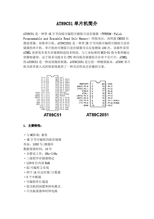
AT89C51单片机简介AT89C51是一种带4K字节闪烁可编程可擦除只读存储器(FPEROM—Falsh Programmable and Erasable Read Only Memory)的低电压,高性能CMOS8位微处理器,俗称单片机。
AT89C2051是一种带2K字节闪烁可编程可擦除只读存储器的单片机。
单片机的可擦除只读存储器可以反复擦除100次。
该器件采用ATMEL高密度非易失存储器制造技术制造,与工业标准的MCS-51指令集和输出管脚相兼容。
由于将多功能8位CPU和闪烁存储器组合在单个芯片中,ATMEL 的AT89C51是一种高效微控制器,AT89C2051是它的一种精简版本。
AT89C单片机为很多嵌入式控制系统提供了一种灵活性高且价廉的方案。
1.主要特性:·与MCS-51 兼容·4K字节可编程闪烁存储器寿命:1000写/擦循环数据保留时间:10年·全静态工作:0Hz-24Hz·三级程序存储器锁定·128*8位内部RAM·32可编程I/O线·两个16位定时器/计数器·5个中断源·可编程串行通道·低功耗的闲置和掉电模式·片内振荡器和时钟电路2.管脚说明:VCC:供电电压。
GND:接地。
P0口:P0口为一个8位漏级开路双向I/O口,每脚可吸收8TTL门电流。
当P1口的管脚第一次写1时,被定义为高阻输入。
P0能够用于外部程序数据存储器,它可以被定义为数据/地址的第八位。
在FIASH编程时,P0 口作为原码输入口,当FIASH进行校验时,P0输出原码,此时P0外部必须被拉高。
P1口:P1口是一个内部提供上拉电阻的8位双向I/O口,P1口缓冲器能接收输出4TTL门电流。
P1口管脚写入1后,被内部上拉为高,可用作输入,P1口被外部下拉为低电平时,将输出电流,这是由于内部上拉的缘故。
在FLASH编程和校验时,P1口作为第八位地址接收。
AT89C51单片机简单介绍

AT89C51单片机简单介绍
AT89C51单片机是一款由Atmel公司生产出的基于8位MCS-51内核架构的单片机。
其内部包含大量的外设和接口,如8KB的Flash存储器、128字节的RAM、32个通用输入/输出引脚、三个16位定时器/计数器,还具备可编程的串行通讯接口UART、SPI、I2C总线控制等外设,使其在嵌入式系统中广泛应用。
AT89C51单片机拥有稳定、可靠的性能,主要应用于各种嵌入式系统中,例如:智能家居、仪器仪表、安防控制设备、工业自动化设备、医疗设备等。
1. 采用MCS-51内核架构,具有8位宽的数据总线和16位宽的地址总线;
2. 内置8KB的Flash存储器和128字节的RAM,可实现程序存储和数据处理;
3. 32个通用输入/输出引脚,可扩展各种外设和接口;
4. 内置三个16位定时器/计数器,可生成多种PWM波形,产生各种延时和定时功能;
5. 内置可编程的串行通讯接口UART,支持RS232、RS485通讯协议;
6. 支持SPI、I2C总线控制,可实现多种通讯方式;
7. 拥有多种中断模式和中断源,可实现多任务处理、多线程操作;
8. 采用低功耗设计,外部器件少,体积小,非常适合嵌入式系统应用。
最后,AT89C51单片机是一款性价比高、应用广泛、可靠稳定的单片机,是嵌入式系统设计师的不二之选。
AT89C51简介
AT89C51简介AT89C51是一种带4K字节FLASH存储器(FPEROM—Flash Programmable and Erasable Read Only Memory)的低电压、高性能CMOS 8位微处理器,俗称单片机。
AT89C2051是一种带2K字节闪存可编程可擦除只读存储器的单片机。
单片机的可擦除只读存储器可以反复擦除1000次。
该器件采用ATMEL高密度非易失存储器制造技术制造,与工业标准的MCS-51指令集和输出管脚相兼容。
由于将多功能8位CPU和闪烁存储器组合在单个芯片中,ATMEL的AT89C51是一种高效微控制器,AT89C2051是它的一种精简版本。
AT89C单片机为很多嵌入式控制系统提供了一种灵活性高且价廉的方案。
外形及引脚排列如图所示编辑本段主要特性:·与MCS-51 兼容·4K字节可编程FLASH存储器·寿命:1000写/擦循环·数据保留时间:10年·全静态工作:0Hz-24MHz·三级程序存储器锁定·128×8位内部RAM·32可编程I/O线·两个16位定时器/计数器·5个中断源·可编程串行通道·低功耗的闲置和掉电模式·片内振荡器和时钟电路编辑本段管脚说明:VCC:供电电压。
GND:接地。
P0口:P0口为一个8位漏级开路双向I/O口,每脚可吸收8TTL门电流。
当P0口的管脚第一次写1时,被定义为高阻输入。
P0能够用于外部程序数据存储器,它可以被定义为数据/地址的第八位。
在FIASH编程时,P0 口作为原码输入口,当FIASH进行校验时,P0输出原码,此时P0外部必须被拉高。
P1口:P1口是一个内部提供上拉电阻的8位双向I/O口,P1口缓冲器能接收输出4TTL门电流。
P1口管脚写入1后,被内部上拉为高,可用作输入,P1口被外部下拉为低电平时,将输出电流,这是由于内部上拉的缘故。
at89c51中文资料_数据手册_参数
万联芯城 电子元器件物料全国供应,专业提 供电子元器件原装现货产品,1 片起订,价格优势明显,电子元 器件采购网万联芯城目前为长电科技,顺络电子,先科 ST 等多 家知名原厂的指定授权代理商,专为客户提供电子元器件配单业 务,提交物料清单即可当天报价当天发货,点击进入万联芯城。
AT89C51是一种低功耗、高性能的CMOS 8位微型计算机,具有4Kbytes的Flash可编程只读 存储器(PEROM)。该设备使用Atmel的高密度非易失性存储器技术制造,与工业标准的 MCS-51指令集和pinout兼容。芯片上的闪存可以让程序内存在系统内重新编程,也可以 由一个召集人的非易失性内存程序员来重新编程。Atmel AT89C51是一种功能强大的微型 计算机,它将一个多用途的8位CPU与闪存芯片结合在一起,为许多嵌入式控制应用程序 提供了一种高灵活性和高性价比的解决方案。AT89C51提供了以下标准特性:4Kbytes的 Flash, 128字节的RAM, 32个I/O行,两AT89C51个16位的计时器/计数器,一个五个矢量的 二级中断架构,一个完整的双工串口,片上振荡器和时钟圈-cuitry。此外,AT89C51采用 静态逻辑设计,可将操பைடு நூலகம்频率降至零,支持两种软件可选择的节能模式。空闲的适当操 作CPU,同时允许RAM、计时器/计数器、串行端口和中断系统继续运行。电源关闭模式 保存RAM内容,但冻结振荡器禁用所有其他芯片功能,直到下一个硬件复位。销 DescriptionVCCSupply voltage.GNDGround。端口0Port 0是一个8位开路双向I/O端口。作为 输出端口,每个引脚可以接收8个TTLAT89C51输入。当1被写入端口0时,这些引脚可以 作为高阻抗输入。端口0也可以配置为在访问外部pro-gram和数据内存期间的多路低阶地 址/数据总线。在这种模式下,P0具有内浆。端口0也在Flash编程期间接收代码字节,并 输出代码字节du环编程验证。AT89C51在程序验证过程中需要外部的pullups。端口1是一 个8位双向I/O端口,具有内部pullups。端口1输出缓冲区可以接收/源4个TTL输入。当1s被 写入端口1引脚时,它们被内部的脉冲拉高,并可作为输入。作为输入,外部被拉低的端 口1引脚会因为内部的pullups而变酸(IIL)。端口1也在flash编程和验证过程中接收低阶地址 字节。端口2Port 2是一个带有内部pullups的8位双向I/O端口。端口2输出缓冲区可以接收/ 源4个TTL输入。当1s被写到端口2时,它们被内部的pullups拉得很高,可以用作输入。作 为输入,外部被拉低的端口2引脚会因为内部的脉冲而变酸。端口2在从外部程序内存获 取和访问使用16位地址的外部数据内存(MOVX @DPTR)期间发出高阶地址字节。在这个 应用中,当发射1s时,它使用强的内部拉升。在访问使用8位地址(MOVX @ RI)的外部数 据存储器时,端口2发出P2专AT89C51用函数寄存器的核心。端口2还在Flash编程和验证 过程中接收高阶地址位和somecontrol信号。端口3Port 3是一个8位双向I/O端口,具有内部 pullups。端口3输出缓冲区可以接收/源四个TTL输入。当1s被写到端口3时,它们被内部的 pullups拉得很高,可以用作输入。作为输入,外部被拉低的端口3引脚会因为pullups而变 酸(IIL)。端口3还具有AT89C51的各种特殊功能,如下所示在每次访问外部数据时都跳过 了pulse。如果需要,可以通过设置sfr位置8EH的0位来禁用ALE操作。在位集上,ALE只 在一个MOVX或MOVC指令中活动。否则,大头针就会弱拉高。如果微控制器处于外部 执行模式,则设置禁用“禁用”的位就没有效果。PSENProgram Store启用的是read strobe 到外部的pro-AT89C51gram内存。当AT89C51执行来自外部pro-gram内存的代码时,每个 machinecycle都会激活PSEN两次,除了在每次访问外部数据内存时跳过两次PSEN激 活。EA / VPPExternal访问启用AT89C51。必须将EA绑定到GND,以使设备能够从从从 0000H到FFFFH的外部pro-gram内存位置获取代码。然而,请注意,如果锁位1被编 程,EA将在复位时被内部锁住。EA应该绑定到VCC以执行内部程序。在Flash编程中,这 个pin还能接收12伏的编程实现volt-age (VPP),这是需要12伏VPP的部件。XTAL1Input输入到逆变振荡器放大器,输入到内部时 钟运行电路。XTAL2Output逆变振荡器放大器的输出。振荡器特性sxtal1和XTAL2分别是 逆变放大器的输入和输出,可以配置为使用asan片上振荡器,如图1所示。可以使用石英 晶体或陶瓷谐振器。要从外部时钟源驱动设备,XTAL2应该保持左连接,而XTAL1应该 被驱动,如图2所示。在外部时钟信号的工作周期中没有要求,因为内部时钟电路的输入 是通过两个触发器,但是最小和最大的电压高AT89C51和低的时间规格必须被观察。在 空闲模式下,CPU自动进入休眠状态,而所有的片上外围设备仍然处于活动状态。模式 是由软件调用的。在此模式下,片上RAM的内容和所有的spe函数寄存器都保持不变。空 闲模式可以通过任何启用的中断或硬件重置来终止。应该注意的是,当空闲被硬件 AT89C51重置终止时,设备通常会恢复程序执行,从它停止的地方开始,直到内部复位 算法控制之前的两个机器周期。在这种情况下,芯片上的硬件存储限制了对内部RAM的 访问,AT89C51但是对端口引脚的访问是不受限制的。为了消除AT89C51在空闲时对端口 pin进行意外写入的可能性,可以通过重置来终止,调用idleshnd的指令后面的指令不应该 是写入端口pin或外部内存的指令
有关单片机AT89C51简介的中英文资料
单片机AT89C51简介AT89C51是美国ATMEL公司生产的低电压,高性能CMOS8位单片机,片内含4Kb字节的快速可擦写的只读程序存储器(PEROM)和128 字节的随机存取数据存储器(RAM),器件采用ATMEL公司的高密度、非易失性存储技术生产,兼容标准MCS-51产品指令系统,片内置通用8位中央处理器(CPU)和Flash存储单元,功能强大AT89C51单片机可为您提供许多高性价比的应用场合,可灵活应用于各种控制领域。
主要性能参数:1)与MCS-51产品指令系统完全兼容;2)4K字节可重复写flash闪速存储器;3)1000次擦写周期;4)全静态操作:0HZ-24MHZ;5)三级加密程序存储器;6)128*8字节内部RAM;7)32个可编程I/O口;8)2个16位定时/计数器;9)6个中断源;10)可编程串行UART通道;11)低功耗空闲和掉电模式。
功能特性概述:AT89C51提供以下标准功能:4K 字节闪速存储器,128字节内部RAM,32个I/O口线,两个16位定时/计数器,一个5向量两级中断结构,一个全双工串行通信口,片内振荡器及时钟电路。
同时,AT89C51可降至0HZ的静态逻辑操作,并支持两种软件可选的节电工作模式。
空闲方式停止CPU的工作,但允许RAM,定时/计数器,串行通信口及中断系统继续工作。
掉电方式保存RAM 中的内容,但振荡器停止工作并禁止其它所有部件工作直到下一个硬件复位。
引脚功能说明:Vcc:电源电压GND:地P0口:P0口是一组8位漏极开路型双向I/O口,也即地址/数据总线复位口。
作为输出口用时,每位能吸收电流的方式驱动8个逻辑门电路,对端口写“1”可作为高阻抗输入端用。
在访问外部数据存储器或程序存储器时,这组口线分时转换地址(低8位)和数据总线复用,在访问期间激活内部上拉电阻。
P1口:P1是一个带内部上拉电阻的8位双向I/O口,P1的输出缓冲级可驱动(吸收或输出电流)4个TTL逻辑门电路。
AT89C51与AT89C52简介
AT89C51简介AT89C51是一种带4K字节FLASH存储器(FPEROM—Flash Programmable and Erasable Read Only Memory)的低电压、高性能CMOS 8位微处理器,俗称单片机。
AT89C2051是一种带2K字节闪存可编程可擦除只读存储器的单片机。
单片机的可擦除只读存储器可以反复擦除1000次。
该器件采用ATMEL高密度非易失存储器制造技术制造,与工业标准的MCS-51指令集和输出管脚相兼容。
由于将多功能8位CPU和闪烁存储器组合在单个芯片中,ATMEL的AT89C51是一种高效微控制器,AT89C2051是它的一种精简版本。
AT89C单片机为很多嵌入式控制系统提供了一种灵活性高且价廉的方案。
外形及引脚排列如图所示主要特性:·与MCS-51 兼容·4K字节可编程FLASH存储器·寿命:1000写/擦循环·数据保留时间:10年·全静态工作:0Hz-24MHz·三级程序存储器锁定·128×8位内部RAM·32可编程I/O线·两个16位定时器/计数器·5个中断源·可编程串行通道·低功耗的闲置和掉电模式·片内振荡器和时钟电路管脚说明:VCC:供电电压。
GND:接地。
P0口:P0口为一个8位漏级开路双向I/O口,每脚可吸收8TTL门电流。
当P0口的管脚第一次写1时,被定义为高阻输入。
P0能够用于外部程序数据存储器,它可以被定义为数据/地址的第八位。
在FIASH编程时,P0 口作为原码输入口,当FIASH进行校验时,P0输出原码,此时P0外部必须被拉高。
P1口:P1口是一个内部提供上拉电阻的8位双向I/O口,P1口缓冲器能接收输出4TTL门电流。
P1口管脚写入1后,被内部上拉为高,可用作输入,P1口被外部下拉为低电平时,将输出电流,这是由于内部上拉的缘故。
- 1、下载文档前请自行甄别文档内容的完整性,平台不提供额外的编辑、内容补充、找答案等附加服务。
- 2、"仅部分预览"的文档,不可在线预览部分如存在完整性等问题,可反馈申请退款(可完整预览的文档不适用该条件!)。
- 3、如文档侵犯您的权益,请联系客服反馈,我们会尽快为您处理(人工客服工作时间:9:00-18:30)。
原文:The Introduction of AT89C51DescriptionThe AT89C51 is a low-power, high-performance CMOS 8-bit microcomputer with 4K bytes of Flash programmable and erasable read only memory (PEROM). The device is manufactured using Atmel’s high-density nonvolatile memory technology and is compatible with the industry-standard MCS-51 instruction set and pinout. The on-chip Flash allows the program memory to be reprogrammed in-system or by a conventional nonvolatile memory programmer. By combining a versatile 8-bit CPU with Flash on a monolithic chip, the Atmel AT89C51 is a powerful microcomputer which provides a highly-flexible and cost-effective solution to many embedded control applications.Function characteristicThe AT89C51 provides the following standard features: 4K bytes of Flash, 128 bytes of RAM, 32 I/O lines, two 16-bit timer/counters, a five vector two-level interrupt architecture, a full duplex serial port, on-chip oscillator and clock circuitry. In addition, the AT89C51 is designed with static logic for operation down to zero frequency and supports two software selectable power saving modes. The Idle Mode stops the CPU while allowing the RAM, timer/counters, serial port and interrupt system to continue functioning. The Power-down Mode saves the RAM contents but freezes the oscillator disabling all other chip functions until the next hardware reset.Pin DescriptionVCC:Supply voltage.GND:Ground.Port 0Port 0 is an 8-bit open-drain bi-directional I/O port. As an output port, each pin can sink eight TTL inputs. When 1s are written to port 0 pins, the pins can be used as highimpedance inputs.Port 0 may also be configured to be the multiplexed loworder address/data bus during accesses to external program and data memory. In this mode P0 has internal pullups.Port 0 also receives the code bytes during Flash programming,and outputs the code bytes during programverification. External pullups are required during programverification.Port 1Port 1 is an 8-bit bi-directional I/O port with internal pullups.The Port 1 output buffers can sink/source four TTL inputs.When 1s are written to Port 1 pins they are pulled high by the internal pullups and can be used as inputs. As inputs,Port 1 pins that are externally being pulled low will source current (IIL) because of the internal pullups.Port 1 also receives the low-order address bytes during Flash programming and verification.Port 2Port 2 is an 8-bit bi-directional I/O port with internal pullups.The Port 2 output buffers can sink/source four TTL inputs.When 1s are written to Port 2 pins they are pulled high by the internal pullups and can be used as inputs. As inputs,Port 2 pins that are externally being pulled low will source current, because of the internal pullups.Port 2 emits the high-order address byte during fetches from external program memory and during accesses to external data memory that use 16-bit addresses. In this application, it uses strong internal pullupswhen emitting 1s. During accesses to external data memory that use 8-bit addresses, Port 2 emits the contents of the P2 Special Function Register.Port 2 also receives the high-order address bits and some control signals during Flash programming and verification.Port 3Port 3 is an 8-bit bi-directional I/O port with internal pullups.The Port 3 output buffers can sink/source four TTL inputs.When 1s are written to Port 3 pins they are pulled high by the internal pullups and can be used as inputs. As inputs,Port 3 pins that are externally being pulled low will source current (IIL) because of the pullups.Port 3 also serves the functions of various special features of the AT89C51 as listed below:Port 3 also receives some control signals for Flash programming and verification.RSTReset input. A high on this pin for two machine cycles while the oscillator is running resets the device.ALE/PROGAddress Latch Enable output pulse for latching the low byte of the address during accesses to external memory. This pin is also the program pulse input (PROG) during Flash programming.In normal operation ALE is emitted at a constant rate of 1/6 the oscillator frequency, and may be used for external timing or clocking purposes. Note, however, that one ALE pulse is skipped during each access to external Data Memory.If desired, ALE operation can be disabled by setting bit 0 of SFR location 8EH. With the bitset, ALE is active only during a MOVX or MOVC instruction. Otherwise, the pin is weakly pulled high. Setting the ALE-disable bit has no effect if the microcontroller is in external execution mode.PSENProgram Store Enable is the read strobe to external program memory.When the AT89C51 is executing code from external program memory, PSEN is activated twice each machine cycle, except that two PSEN activations are skipped during each access to external data memory.EA/VPPExternal Access Enable. EA must be strapped to GND in order to enable the device to fetch code from external program memory locations starting at 0000H up to FFFFH. Note, however, that if lock bit 1 is programmed, EA will be internally latched on reset.EA should be strapped to VCC for internal program executions.This pin also receives the 12-volt programming enable voltage(VPP) during Flash programming, for parts that require12-volt VPP.XTAL1Input to the inverting oscillator amplifier and input to the internal clock operating circuit.XTAL2Output from the inverting oscillator amplifier.Oscillator CharacteristicsXTAL1 and XTAL2 are the input and output, respectively,of an inverting amplifier which can be configured for use as an on-chip oscillator, as shown in Figure 1.Either a quartz crystal or ceramic resonator may be used. To drive the device from an external clock source, XTAL2 should be left unconnected while XTAL1 is driven as shown in Figure 2.There are no requirements on the duty cycle of the external clock signal, since the input to the internal clocking circuitry is through a divide-by-two flip-flop, but minimum and maximum voltage high and low time specifications must be observed.Figure 1. Oscillator Connections Figure 2. External Clock Drive ConfigurationIdle ModeIn idle mode, the CPU puts itself to sleep while all the onchip peripherals remain active. The mode is invoked by software. The content of the on-chip RAM and all the special functions registers remain unchanged during this mode. The idle mode can be terminated by any enabled interrupt or by a hardware reset.It should be noted that when idle is terminated by a hard ware reset, the device normally resumes program execution,from where it left off, up to two machine cycles before the internal reset algorithm takes control. On-chip hardware inhibits access to internal RAM in this event, but access to the port pins is not inhibited. To eliminate the possibility of an unexpected write to a port pin when Idle is terminated by reset,the instruction following the one that invokes Idle should not be one that writes to a port pin or to external memory.Power-down ModeIn the power-down mode, the oscillator is stopped, and the instruction that invokes power-down is the last instruction executed. The on-chip RAM and Special Function Registers retain their values until the power-down mode is terminated. The only exit from power-down is a hardware reset. Reset redefines the SFRs but does not change the on-chip RAM. The reset should not be activated before VCC is restored to its normal operating level and must be held active long enough to allow the oscillator to restart and stabilize.Program Memory Lock BitsOn the chip are three lock bits which can be left unprogrammed (U) or can be programmed (P) to obtain the additional features listed in the table below.When lock bit 1 is programmed, the logic level at the EA pin is sampled and latched during reset. If the device is powered up without a reset, the latch initializes to a random value, and holds that value until reset is activated. It is necessary that the latched value of EA be in agreement with the current logic level at that pin in order for the device to functionproperly.译文:AT89C51的介绍描述AT89C51是一个低电压,高性能CMOS 8位单片机带有4K字节的可反复擦写的程序存储器(PENROM)。