Signature of the solar cycle in the low degree p-modes using Mark-I
烟雾传感器JTY-GD-CA2001L使用说明书

The JTY-GD-CA2001L Photoelectric Smoke Detector is suitable for Many such places As kinds of environments, mall,entertainment
Relative Humidity: ≤95%RH(40℃±2℃) Output Method: Sound and light alarm Non-source point transmitting
2. Functions
Threshold of the fire alarm, the detector will start to intelligent examining with the light sparkling. If the examining result attains to the threshold of the alarm, the light of the detector will be bright, and the system will startup the relay. When the smoke falls to the threshold of the alarm, the detector will come back the normal situation.
Smoke Alarm: In the normal situation, the instruction light of detector will be bright every 20 seconds aut omatically. The detector will self-examine the smoke in the room every 1.6second. when the smoke attains to the
MX25L512MC-12G中文资料

MX25L512512K-BIT [x 1] CMOS SERIAL FLASH FEATURESGENERAL• Serial Peripheral Interface (SPI) compatible -- Mode 0 and Mode 3• 524,288 x 1 bit structure• 16 Equal Sectors with 4K byte each- Any Sector can be erased individually• S ingle Power Supply Operation- 2.7 to 3.6 volt for read, erase, and program operations• L atch-up protected to 100mA from -1V to Vcc +1VPERFORMANCE• H igh Performance- Fast access time: 85MHz serial clock (15pF + 1TTL Load) and 66MHz serial clock (30pF + 1TTL Load)- Fast program time: 1.4ms(typ.) and 5ms(max.)/page (256-byte per page)- Fast erase time: 60ms(typ.) and 120ms(max.)/sector (4K-byte per sector) ; 1s(typ.) and 2s(max.)/chip(512Kb)• L ow Power Consumption- Low active read current: 12mA(max.) at 85MHz, 8mA(max.) at 66MHz and 4mA(max.) at 33MHz- Low active programming current: 15mA (max.)- Low active erase current: 15mA (max.)- Low standby current: 10uA (max.)- Deep power-down mode 1uA (typical)• M inimum 100,000 erase/program cyclesSOFTWARE FEATURES• Input Data Format- 1-byte Command code• Block Lock protection- The BP0~BP1 status bit defines the size of the area to be software protected against Program and Erase in-structions.• Auto Erase and Auto Program Algorithm- Automatically erases and verifies data at selected sector- Automatically programs and verifies data at selected page by an internal algorithm that automatically times the program pulse widths (Any page to be programed should have page in the erased state first)• Status Register Feature• Electronic Identification- JEDEC 2-byte Device ID- RES command, 1-byte Device IDHARDWARE FEATURES• SCLK Input- Serial clock input• SI Input- Serial Data Input• SO Output- Serial Data Output• WP# pin- Hardware write protection• HOLD# pin- pause the chip without diselecting the chip• PACKAGE- 8-pin SOP (150mil)- 8-USON (2x3mm)- All Pb-free devices are RoHS CompliantGENERAL DESCRIPTIONMX25L512 is a CMOS 524,288 bit serial Flash memory, which is configured as 65,536 x 8 internally. MX25L512 features a serial peripheral interface and software protocol allowing operation on a simple 3-wire bus. The three bus signals are a clock input (SCLK), a serial data input (SI), and a serial data output (SO). SPI access to the device is enabled by CS# input.MX25L512 provide sequential read operation on whole chip.After program/erase command is issued, auto program/ erase algorithms which program/ erase and verify the spec-ified page or sector/block locations will be executed. Program command is executed on page (256 bytes) basis, and erase command is executes on chip or sector (4K-bytes).To provide user with ease of interface, a status register is included to indicate the status of the chip. The status read command can be issued to detect completion status of a program or erase operation via WIP bit.When the device is not in operation and CS# is high, it is put in standby mode and draws less than 10uA DC cur-rent.The MX25L512 utilize MXIC's proprietary memory cell, which reliably stores memory contents even after 100,000 program and erase cycles.PIN CONFIGURATIONSSYMBOL DESCRIPTION CS#Chip SelectSI Serial Data Input SO Serial Data Output SCLK Clock InputHOLD#Hold, to pause the device without deselecting the device WP#Write ProtectionVCC + 3.3V Power Supply GNDGroundPIN DESCRIPTION8-PIN SOP (150mil)CS#SO WP#GND VCC HOLD#SCLK SI8-LAND USON (2x3mm)CS#SO WP#GND VCC HOLD#SCLK SIBLOCK DIAGRAMDATA PROTECTIONMX25L512 is designed to offer protection against accidental erasure or programming caused by spurious system level signals that may exist during power transition. During power up the device automatically resets the state ma-chine in the standby mode. In addition, with its control register architecture, alteration of the memory contents only occurs after successful completion of specific command sequences. The device also incorporates several features to prevent inadvertent write cycles resulting from VCC power-up and power-down transition or system noise.• Valid command length checking: The command length will be checked whether it is at byte base and completed on byte boundary.• Write Enable (WREN) command: WREN command is required to set the Write Enable Latch bit (WEL) before other command to change data. The WEL bit will return to reset stage under following situation:- Power-up- Write Disable (WRDI) command completion- Write Status Register (WRSR) command completion- Page Program (PP) command completion- Sector Erase (SE) command completion- Block Erase (BE) command completion- Chip Erase (CE) command completion• Software Protection Mode (SPM): by using BP0-BP1 bits to set the part of Flash protected from data change.• Hardware Protection Mode (HPM): by using WP# going low to protect the BP0-BP1 bits and SRWD bit from data change.• Deep Power Down Mode: By entering deep power down mode, the flash device also is under protected from writing all commands except Release from deep power down mode command (RDP) and Read Electronic Sig-nature command (RES).Table 1. Protected Area SizesStatus bitProtect level 512b BP1 BP00 0 0 (none) None 0 1 1 (All)All 1 0 2 (All)All 113 (All)AllHOLD FEATUREHOLD# pin signal goes low to hold any serial communications with the device. The HOLD feature will not stop the operation of write status register, programming, or erasing in progress.The operation of HOLD requires Chip Select(CS#) keeping low and starts on falling edge of HOLD# pin signal while Serial Clock (SCLK) signal is being low (if Serial Clock signal is not being low, HOLD operation will not start until Serial Clock signal being low). The HOLD condition ends on the rising edge of HOLD# pin signal while Se-rial Clock(SCLK) signal is being low( if Serial Clock signal is not being low, HOLD operation will not end until Serial Clock being low), see Figure 1.The Serial Data Output (SO) is high impedance, both Serial Data Input (SI) and Serial Clock (SCLK) are don't care during the HOLD operation. If Chip Select (CS#) drives high during HOLD operation, it will reset the internal logic of the device. To re-start communication with chip, the HOLD# must be at high and CS# must be at low.Figure 1. Hold Condition OperationTable 2. COMMAND DEFINITION(1) ADD=00H will output the manufacturer's ID first and ADD=01H will output device ID first.(2) BE command may erase whole 512Kb chip.(3) It is not recommended to adopt any other code which is not in the above command definition table.COMMAND (byte)WREN (write enable)WRDI (write disable)RDID (readidentification)RDSR (read status register)WRSR (write status register)READ(read data)Fast Read(fast readdata)1st 06 (hex)04 (hex)9F (hex)05 (hex)01 (hex)03 (hex)0B (hex)2nd AD1AD13rd AD2AD24th AD3AD35th xActionsets the (WEL) write enable latch bit resets the (WEL) write enable latchbit outputs manufacturer ID and 2-byte device IDto read out the status register to write new values to the status register n bytes read out until CS# goes highCOMMAND (byte)SE(Sector Erase)BE (2)(Block Erase)CE (Chip Erase)PP(Page Program)DP(Deep Power Down) RDP(Release from Deep Power-down) RES (ReadElectronicID)REMS (ReadElectronicManufacturer& Device ID)1st 20 (hex)52 or D8 (hex)60 or C7 (hex)02 (hex) B9 (hex)AB (hex)AB (hex)90 (hex)2nd AD1AD1AD1x x 3rd AD2AD2AD2x x 4th AD3AD3AD3xADD(1)5th ActionOutput the manufacturer ID and deviceIDDEVICE OPERATION1. Before a command is issued, status register should be checked to ensure device is ready for the intended op-eration.2. When incorrect command is inputted to this LSI, this LSI becomes standby mode and keeps the standby modeuntil next CS# falling edge. In standby mode, SO pin of this LSI should be High-Z.3. When correct command is inputted to this LSI, this LSI becomes active mode and keeps the active mode until next CS# rising edge.4. Input data is latched on the rising edge of Serial Clock(SCLK) and data shifts out on the falling edge of SCLK. The difference of SPI mode 0 and mode 3 is shown as Figure 2.Figure 2. SPI Modes SupportedSCLKMSBCPHA shift inshift outSI 01CPOL(Serial mode 0)(Serial mode 3)1SO SCLKMSB5. For the following instructions: RDID, RDSR, READ, FAST_READ, RES and REMS the shifted-in instruction se-quence is followed by a data-out sequence. After any bit of data being shifted out, the CS# can be high. For the following instructions: WREN, WRDI, WRSR, SE, BE, CE, PP , RDP and DP the CS# must go high exactly at the byte boundary; otherwise, the instruction will be rejected and not executed.6. During the progress of Write Status Register, Program, Erase operation, to access the memory array is neglect-ed and not affect the current operation of Write Status Register, Program, Erase. Table 3. Memory OrganizationNote:CPOL indicates clock polarity of SPI master, CPOL=1 for SCLK high while idle, CPOL=0 for SCLK low while not transmitting. CPHA indicates clock phase. The combination of CPOL bit and CPHA bit decides which SPI mode is supported.Sector Address Range1500F000h 00FFFFh:::3003000h 003FFFh 2002000h 002FFFh 1001000h 001FFFh 0000000h 000FFFhCOMMAND DESCRIPTION(1) Write Enable (WREN)The Write Enable (WREN) instruction is for setting Write Enable Latch (WEL) bit. For those instructions like PP, SE, BE, CE, and WRSR, which are intended to change the device content, should be set every time after the WREN in-struction setting the WEL bit.The sequence of issuing WREN instruction is: CS# goes low-> sending WREN instruction code-> CS# goes high. (see Figure 11)(2) Write Disable (WRDI)The Write Disable (WRDI) instruction is for resetting Write Enable Latch (WEL) bit.The sequence of issuing WRDI instruction is: CS# goes low-> sending WRDI instruction code-> CS# goes high. (see Figure 12)The WEL bit is reset by following situations:- Power-up- Write Disable (WRDI) instruction completion- Write Status Register (WRSR) instruction completion- Page Program (PP) instruction completion- Sector Erase (SE) instruction completion- Block Erase (BE) instruction completion- Chip Erase (CE) instruction completion(3) Read Identification (RDID)RDID instruction is for reading the manufacturer ID of 1-byte and followed by Device ID of 2-byte. The MXIC Manu-facturer ID is C2(hex), the memory type ID is 20(hex) as the first-byte device ID, and the individual device ID of second-byte ID is as followings: 10(hex) for MX25L512.The sequence of issuing RDID instruction is: CS# goes low→sending RDID instruction code→24-bits ID data out on SO→to end RDID operation can use CS# to high at any time during data out. (see Figure. 13)While Program/Erase operation is in progress, it will not decode the RDID instruction, so there's no effect on the cy-cle of program/erase operation which is currently in progress. When CS# goes high, the device is at standby stage.(4) Read Status Register (RDSR)The RDSR instruction is for reading Status Register Bits. The Read Status Register can be read at any time (even in program/erase/write status register condition) and continuously. It is recommended to check the Write in Progress (WIP) bit before sending a new instruction when a program, erase, or write status register operation is in progress. The sequence of issuing RDSR instruction is: CS# goes low→sending RDSR instruction code→Status Register data out on SO (see Figure. 14)The definition of the status register bits is as below:WIP bit. The Write in Progress (WIP) bit, a volatile bit, indicates whether the device is busy in program/erase/write status register progress. When WIP bit sets to 1, which means the device is busy in program/erase/write status register progress. When WIP bit sets to 0, which means the device is not in progress of program/erase/write status register cycle.WEL bit. The Write Enable Latch (WEL) bit, a volatile bit, indicates whether the device is set to internal write enable latch. When WEL bit sets to 1, which means the internal write enable latch is set, the device can accept program/erase/write status register instruction. When WEL bit sets to 0, which means no internal write enable latch; the de-vice will not accept program/erase/write status register instruction.BP1, BP0 bits. The Block Protect (BP1, BP0) bits, non-volatile bits, indicate the protected area(as defined in table 1) of the device to against the program/erase instruction without hardware protection mode being set. To write the Block Protect (BP1, BP0) bits requires the Write Status Register (WRSR) instruction to be executed. Those bits define the protected area of the memory to against Page Program (PP), Sector Erase (SE), Block Erase (BE) and Chip Erase(CE) instructions (only if all Block Protect bits set to 0, the CE instruction can be executed)SRWD bit. The Status Register Write Disable (SRWD) bit, non-volatile bit, is operated together with Write Protec-tion (WP#) pin for providing hardware protection mode. The hardware protection mode requires SRWD sets to 1 and WP# pin signal is low stage. In the hardware protection mode, the Write Status Register (WRSR) instruction is no longer accepted for execution and the SRWD bit and Block Protect bits (BP1, BP0) are read only.Note: 1. See the table "Protected Area Sizes".2. The endurance cycles of protect bits are 100,000 cycles; however, the tW time out spec of protect bits isrelaxed as tW = N x 15ms (N is a multiple of 10,000 cycles, ex. N = 2 for 20,000 cycles) after 10,000 cycles on those bits.bit7bit6bit5bit4bit3bit2bit1bit0SRWD (status register write protect)0BP1 (level of protected block)BP0 (level of protected block)WEL (write enable latch)WIP (write inprogress bit)1=status register write disable(note 1)(note 1)1=write enable 0=not write enable 1=write operation 0=not in write operation(5) Write Status Register (WRSR)The WRSR instruction is for changing the values of Status Register Bits. Before sending WRSR instruction, the Write Enable (WREN) instruction must be decoded and executed to set the Write Enable Latch (WEL) bit in ad-vance. The WRSR instruction can change the value of Block Protect (BP1, BP0) bits to define the protected area of memory (as shown in table 1). The WRSR also can set or reset the Status Register Write Disable (SRWD) bit in accordance with Write Protection (WP#) pin signal. The WRSR instruction cannot be executed once the Hardware Protected Mode (HPM) is entered.The sequence of issuing WRSR instruction is: CS# goes low-> sending WRSR instruction code-> Status Register data on SI-> CS# goes high. (see Figure 15)The WRSR instruction has no effect on b6, b5, b4, b1, b0 of the status register.The CS# must go high exactly at the byte boundary; otherwise, the instruction will be rejected and not executed. The self-timed Write Status Register cycle time (tW) is initiated as soon as Chip Select (CS#) goes high. The Write in Progress (WIP) bit still can be check out during the Write Status Register cycle is in progress. The WIP sets 1 during the tW timing, and sets 0 when Write Status Register Cycle is completed, and the Write Enable Latch (WEL) bit is reset.Table 4. Protection ModesNote:1. As defined by the values in the Block Protect (BP1, BP0) bits of the Status Register, as shown in Table 1.As the table above showing, the summary of the Software Protected Mode (SPM) and Hardware Protected Mode (HPM). Software Protected Mode (SPM):- When SRWD bit=0, no matter WP# is low or high, the WREN instruction may set the WEL bit and can changethe values of SRWD, BP1, BP0. The protected area, which is defined by BP1, BP0, is at software protected mode (SPM).- When SRWD bit=1 and WP# is high, the WREN instruction may set the WEL bit can change the values ofSRWD, BP1, BP0. The protected area, which is defined by BP1, BP0, is at software protected mode (SPM)ModeStatus register condition WP# and SRWD bit status Memory Software protectionmode (SPM)Status register can be written in (WEL bit is set to "1") andthe SRWD, BP0-BP1bits can be changed WP#=1 and SRWD bit=0, or WP#=0 and SRWD bit=0, or WP#=1 and SRWD=1The protected areacannotbe program or erase.Hardware protectionmode (HPM)The SRWD, BP0-BP1 of status register bits cannot bechangedWP#=0, SRWD bit=1The protected areacannotbe program or erase.Note: If SRWD bit=1 but WP# is low, it is impossible to write the Status Register even if the WEL bit has previously been set. It is rejected to write the Status Register and not be executed.Hardware Protected Mode (HPM):- When SRWD bit=1, and then WP# is low (or WP# is low before SRWD bit=1), it enters the hardware protected mode (HPM). The data of the protected area is protected by software protected mode by BP1, BP0 and hard-ware protected mode by the WP# to against data modification.Note: to exit the hardware protected mode requires WP# driving high once the hardware protected mode is entered. If the WP# pin is permanently connected to high, the hardware protected mode can never be entered; only can use software protected mode via BP1, BP0.(6) Read Data Bytes (READ)The read instruction is for reading data out. The address is latched on rising edge of SCLK, and data shifts out on the falling edge of SCLK at a maximum frequency fR. The first address byte can be at any location. The address is automatically increased to the next higher address after each byte data is shifted out, so the whole memory can be read out at a single READ instruction. The address counter rolls over to 0 when the highest address has been reached.The sequence of issuing READ instruction is: CS# goes low→ sending READ instruction code→ 3-byte address on SI→ data out on SO→ to end READ operation can use CS# to high at any time during data out. (see Figure. 16) (7) Read Data Bytes at Higher Speed (FAST_READ)The FAST_READ instruction is for quickly reading data out. The address is latched on rising edge of SCLK, and data of each bit shifts out on the falling edge of SCLK at a maximum frequency fC. The first address byte can be at any location. The address is automatically increased to the next higher address after each byte data is shifted out, so the whole memory can be read out at a single FAST_READ instruction. The address counter rolls over to 0 when the highest address has been reached.The sequence of issuing FAST_READ instruction is: CS# goes low→ sending FAST_READ instruction code→ 3-byte address on SI→ 1-dummy byte address on SI→data out on SO→ to end FAST_READ operation can use CS# to high at any time during data out. (see Figure. 17)While Program/Erase/Write Status Register cycle is in progress, FAST_READ instruction is rejected without any im-pact on the Program/Erase/Write Status Register current cycle.(8) Sector Erase (SE)The Sector Erase (SE) instruction is for erasing the data of the chosen sector to be "1". A Write Enable (WREN) in-struction must execute to set the Write Enable Latch (WEL) bit before sending the Sector Erase (SE). Any address of the sector (see table 3) is a valid address for Sector Erase (SE) instruction. The CS# must go high exactly at the byte boundary (the latest eighth of address byte been latched-in); otherwise, the instruction will be rejected and not executed.Address bits [Am-A12] (Am is the most significant address) select the sector address.The sequence of issuing SE instruction is: CS# goes low → sending SE instruction code→ 3-byte address on SI → CS# goes high. (see Figure 19)The self-timed Sector Erase Cycle time (tSE) is initiated as soon as Chip Select (CS#) goes high. The Write in Progress (WIP) bit still can be check out during the Sector Erase cycle is in progress. The WIP sets 1 during the tSE timing, and sets 0 when Sector Erase Cycle is completed, and the Write Enable Latch (WEL) bit is reset. If the page is protected by BP1, BP0 bits, the Sector Erase (SE) instruction will not be executed on the page.(9) Block Erase (BE)The Block Erase (BE) instruction is for erasing the data of the chosen block to be "1". A Write Enable (WREN) in-struction must execute to set the Write Enable Latch (WEL) bit before sending the Block Erase (BE). Any address of the block (see table 3) is a valid address for Block Erase (BE) instruction. The CS# must go high exactly at the byte boundary (the latest eighth of address byte been latched-in); otherwise, the instruction will be rejected and not executed.The sequence of issuing BE instruction is: CS# goes low → sending BE instruction code→ 3-byte address on SI → CS# goes high. (see Figure 20)The self-timed Block Erase Cycle time (tBE) is initiated as soon as Chip Select (CS#) goes high. The Write in Progress (WIP) bit still can be check out during the Sector Erase cycle is in progress. The WIP sets 1 during the tBE timing, and sets 0 when Sector Erase Cycle is completed, and the Write Enable Latch (WEL) bit is reset. If the page is protected by BP1, BP0 bits, the Block Erase (BE) instruction will not be executed on the page.(10) Chip Erase (CE)The Chip Erase (CE) instruction is for erasing the data of the whole chip to be "1". A Write Enable (WREN) instruc-tion must execute to set the Write Enable Latch (WEL) bit before sending the Chip Erase (CE). Any address of the sector (see table 3) is a valid address for Chip Erase (CE) instruction. The CS# must go high exactly at the byte boundary( the latest eighth of address byte been latched-in); otherwise, the instruction will be rejected and not ex-ecuted.The sequence of issuing CE instruction is: CS# goes low→ sending CE instruction code→ CS# goes high. (see Figure 20)The self-timed Chip Erase Cycle time (tCE) is initiated as soon as Chip Select (CS#) goes high. The Write in Progress (WIP) bit still can be check out during the Chip Erase cycle is in progress. The WIP sets 1 during the tCE timing, and sets 0 when Chip Erase Cycle is completed, and the Write Enable Latch (WEL) bit is reset. If the chip is protected by BP1, BP0 bits, the Chip Erase (CE) instruction will not be executed. It will be only executed when BP1, BP0 all set to "0".(11) Page Program (PP)The Page Program (PP) instruction is for programming the memory to be "0". A Write Enable (WREN) instruction must execute to set the Write Enable Latch (WEL) bit before sending the Page Program (PP). If the eight least sig-nificant address bits (A7-A0) are not all 0, all transmitted data which goes beyond the end of the current page are programmed from the start address if the same page (from the address whose 8 least significant address bits (A7-A0) are all 0). The CS# must keep during the whole Page Program cycle. The CS# must go high exactly at the byte boundary( the latest eighth of address byte been latched-in); otherwise, the instruction will be rejected and not executed. If more than 256 bytes are sent to the device, the data of the last 256-byte is programmed at the request page and previous data will be disregarded. If less than 256 bytes are sent to the device, the data is programmed at the request address of the page without effect on other address of the same page.The sequence of issuing PP instruction is: CS# goes low→ sending PP instruction code→ 3-byte address on SI→at least 1-byte on data on SI→ CS# goes high. (see Figure 18)The self-timed Page Program Cycle time (tPP) is initiated as soon as Chip Select (CS#) goes high. The Write in Progress (WIP) bit still can be check out during the Page Program cycle is in progress. The WIP sets 1 during the tPP timing, and sets 0 when Page Program Cycle is completed, and the Write Enable Latch (WEL) bit is reset. If the page is protected by BP1, BP0 bits, the Page Program (PP) instruction will not be executed.(12) Deep Power-down (DP)The Deep Power-down (DP) instruction is for setting the device on the minimizing the power consumption (to enter-ing the Deep Power-down mode), the standby current is reduced from ISB1 to ISB2). The Deep Power-down mode requires the Deep Power-down (DP) instruction to enter, during the Deep Power-down mode, the device is not ac-tive and all Write/Program/Erase instruction are ignored. When CS# goes high, it's only in standby mode not deep power-down mode. It's different from Standby mode.The sequence of issuing DP instruction is: CS# goes low→ sending DP instruction code→ CS# goes high. (see Fig-ure 22)Once the DP instruction is set, all instruction will be ignored except the Release from Deep Power-down mode (RDP) and Read Electronic Signature (RES) instruction. (RES instruction to allow the ID been read out). When Power-down, the deep power-down mode automatically stops, and when power-up, the device automatically is in standby mode. For RDP instruction the CS# must go high exactly at the byte boundary (the latest eighth bit of instruction code been latched-in); otherwise, the instruction will not executed. As soon as Chip Select (CS#) goes high, a delay of tDP is required before entering the Deep Power-down mode and reducing the current to ISB2.(13) Release from Deep Power-down (RDP), Read Electronic Signature (RES)The Release from Deep Power-down (RDP) instruction is terminated by driving Chip Select (CS#) High. When Chip Select (CS#) is driven High, the device is put in the Stand-by Power mode. If the device was not previously in the Deep Power-down mode, the transition to the Stand-by Power mode is immediate. If the device was previously in the Deep Power-down mode, though, the transition to the Stand-by Power mode is delayed by tRES2, and Chip Select (CS#) must remain High for at least tRES2(max), as specified in Table 6. Once in the Stand-by Power mode, the device waits to be selected, so that it can receive, decode and execute instructions.RES instruction is for reading out the old style of 8-bit Electronic Signature, whose values are shown as table of ID Definitions. This is not the same as RDID instruction. It is not recommended to use for new design. For new deisng, please use RDID instruction. Even in Deep power-down mode, the RDP and RES are also allowed to be executed, only except the device is in progress of program/erase/write cycle; there's no effect on the current program/erase/ write cycle in progress.The sequence is shown as Figure 23,24.The RES instruction is ended by CS# goes high after the ID been read out at least once. The ID outputs repeat-edly if continuously send the additional clock cycles on SCLK while CS# is at low. If the device was not previously in Deep Power-down mode, the device transition to standby mode is immediate. If the device was previously in Deep Power-down mode, there's a delay of tRES2 to transit to standby mode, and CS# must remain to high at least tRES2(max). Once in the standby mode, the device waits to be selected, so it can be receive, decode, and execute instruction.The RDP instruction is for releasing from Deep Power Down Mode.(14) Read Electronic Manufacturer ID & Device ID (REMS)The REMS instruction is an alternative to the Release from Power-down/Device ID instruction that provides both the JEDEC assigned manufacturer ID and the specific device ID.The REMS instruction is very similar to the Release from Power-down/Device ID instruction. The instruction is initi-ated by driving the CS# pin low and shift the instruction code "90h" followed by two dummy bytes and one bytes address (A7~A0). After which, the Manufacturer ID for MXIC (C2h) and the Device ID are shifted out on the falling edge of SCLK with most significant bit (MSB) first as shown in figure 25. The Device ID values are listed in Table of ID Definitions on page 16. If the one-byte address is initially set to 01h, then the device ID will be read first and then followed by the Manufacturer ID. The Manufacturer and Device IDs can be read continuously, alternating from one to the other. The instruction is completed by driving CS# high.Table of ID Definitions:RDID Command manufacturer ID memory type memory density C22010RES Command electronic ID05REMS Command manufacturer ID device ID C205。
Blue Yeti X 高级 USB 麦克风 快速入门指南说明书

YETI X SOFTWARE CONTROLBLUE SHERPAThe Blue Sherpa companion app can be used to keep your Yeti X firmware up to date and control Yeti X’s features like mic gain, pickup pattern, headphone volume, mute and blend right from your desktop. Download Sherpa here.BLUE VO!CEBlue VO!CE is a suite of real-time audio effects that process your voice for instant professional sound. Use professional, easy-to-use effects including EQ, compression, noise reduction, gate, de-esser and limiter to tailor and sweeten your voice. With Blue VO!CE*, you can make Yeti X sound the way you want using presets for crisp and modern, warm and vintage, classic radio voice, or make your own unique signature sound.Visit /yetix for more details about Blue VO!CE. Blue VO!CE includes DTS audio enhancements.LOGITECH G HUBG HUB is a software platform that gives you control of all your Logitech G products in one place. G HUB is also compatible with Yeti X, giving you access to Blue VO!CE broadcast vocal effects and customized LED lighting features. Download G HUB here.LED LIGHT CUSTOMIZATIONPersonalize the color of Yeti X’s LED lights to match your on-stream aesthetic using Logitech’s free G HUB platform. Yeti X features customizable LED light zones, including the LED rings on and around the Smart Knob, the pickup pattern LED lights and more. Each of the zones can easily be set to any RGB color via the color selector. You can even save different settings to the list at the bottom of the page so you can switch between different colors.Yeti X is compatible with the Blue Sherpa companion app and Logitech G HUB software,giving you deeper control of your mic and access to Blue VO!CE broadcast vocal effects*.* Requires download and installation of Logitech G HUB ()34YETI X AT A GLANCEFOUR-CAPSULE ARRAYYeti X features an all-new four-capsule condenser array, which delivers four pickup patterns with greater focus and clarity than ever.MULTI-FUNCTION SMART KNOBControls key features including microphone gain, mute, headphone volume and Blend balance. See the Multi-Function Smart Knob section for more information.11-SEGMENT LED METERVisualize your voice level with the Yeti X microphone’s 11-segment LED meter. At a glance you can check if your voice level is too high or too low and adjust accordingly. See the Multi-Function Smart Knob and Logitech G HUB Integration sections for more information.PICKUP PATTERN SELECTORCycles between Yeti X’s four pickup patterns. Simply press the button to cycle through each setting in this order: stereo, omni, cardioid and B CONNECTIONAllows Yeti X to connect to your computer. Compatible with USB 1.1, USB 2, and USB 3.HEADPHONE OUTPUT3.5mm (approx. 1/8”) headphone jack. MOUNTING OPTIONSStandard 5/8” threading, compatible with any standard microphone stand as well as accessories like the Compass broadcast boom arm and the Radius III shockmount.INTEGRATED DESKTOP STANDProvides a sturdy base and allows you to tilt the mic up or down toward the sound source for optimal sound quality. By unscrewing the thumb screws on the side, Yeti X can be removed from its base for use with mic stands and accessories.1 2 3 4567856One of Yeti X’s most powerful features is its revolutionary multi-function smart knob, which gives you instant control of essential functions, right at your fingertips. The 11-segment LED meter around the knob displays important information at a glance, helping you maintain professional sound while recording or streaming.FACTORY RESET PROCEDURETo reset Yeti X to factory default settings, press and hold the smart knob and pattern selector buttons while plugging in the USB cable. Continue holding the buttons for 10 seconds and the mute light will flash, indicating Yeti X has been reset.DEFAULT SETTINGS:• Pattern: Cardioid • Gain: 50%• Headphone volume: 50%• Blend: 50/50• Sample rate: 48 kHz • Bit depth: 24SMART KNOB CONTROLS• Turn the knob to adjust gain, headphone volume and Blend settings.• Press the knob once briefly to mute or unmute the microphone signal at any time.• Press and hold the smart knob for one second to switch between modesMULTI-FUNCTION SMART KNOB AND LED METERING7MODE 1: MICROPHONE GAIN AND METERINGWhen the microphone symbol on the left is lit, the smart knob will control Yeti X’s microphone gain, and the meters will show the peak level of the signal in real time with green, yellow and red LEDs. When you move the knob to increase or decrease gain, the meter will temporarily change to blue, showing the gain level you are setting. For the best sound, set the gain so that your loudest speech peaks at the first or second yellow light. Stay away from the red light, but be sure you are regularly filling up all of the green lights. When muted, the green ring on the face of the knob will change to red. Muting and unmuting works in all modes.Press the Smart Knob for one second to get to Headphone Volume mode. Mode selection is ‘sticky’, meaning Yeti X will remain in the mode you select until you change it again.MODE 2: HEADPHONE VOLUMEWhen the headphone symbol on the right side is lit, the smart knob will control the volume of Yeti X’s headphone output, with white LEDs displaying the current level. When you move the knob to adjust the headphone volume, the LEDs will brighten, then dim two seconds after you release the knob.Press the Smart Knob for one second to get to Blend.MODE 3: BLENDWhen both the microphone and headphone symbols are lit, the smart knob is set to adjust the blend between the microphone signal and the sound from your computer in your headphones. By default, the Blend control is set to 50/50 with the white LED centered and the other LEDs unlit. As you turn the knob towards the appropriate icon, magenta LEDs will start filling in from the center. This is useful when you needto hear yourself clearly above the audio from a game, for example.CARDIOIDPerfect for podcasting, game streaming, Skype or Discord calls, vocals and instruments, the cardioid setting captures sound sources that are directly in front of the microphone with a rich, full-bodied sound. The cardioid setting rejects sound coming from directly behind the mic, reducing background noise.OMNIShort for ‘omnidirectional’, the omni setting picks up sound equally from all around the mic. It’s best used in situations when you want to capture the ambience of ‘being there,’ like a conference call or a podcast with multiple people around a table.BIDIRECTIONALThe bidirectional setting records from both the front and the rear of the microphone, which is ideal for podcasting or streaming interviews between two people. The bidirectional setting produces narrow areas of sensitivity and minimizes noise coming from the sides.STEREOThe stereo setting uses both the left and right channels, and is ideal for capturing a realistic sound image when there are multiple sound sourcesin front of the mic. This is useful for multi-person podcasts and immersive experiences like ASMR.Yeti X can be used in four different settings, called pickup patterns (also known as polar patterns). Pickup patterns represent the directions that the microphone will (or won’t) pick up sound from, and each has its own uses.PICKUP PATTERNS89Designed in USA. Made in China.YETI X SPECIFICATIONSSYSTEM REQUIREMENTSPower Required/Consumption: 62mA – 203mA Sample/Bit Rate: 48 kHz, 24-bitCapsules: 4 Blue-proprietary 14mm condenser capsules Polar Patterns: Cardioid, Omnidirectional, Bidirectional, StereoFrequency Response: 20Hz – 20kHz Max SPL: 122dBHEADPHONE AMPLIFIERImpedance: 13 Ohms min, 16 Ohms typical Power Output (RMS): 72mWrms per channel Frequency Response: 20Hz – 20kHz Signal to Noise: 100dBDimensions (extended in stand):4.33” (11cm) x 4.80” (12.2cm) x 11.38” (28.9cm)Weight (microphone and stand): 2.8 lbs (1.28kg)Weight (microphone only): 1.14 lbs (.519kg)WINDOWSWindows 7, 8.1, 10USB 1.1/2.0/3.0MACINTOSHmacOS (10.10 or higher)USB 1.1/2.0/3.010©2019 Blue Microphones. All rights reserved. Blue Logo Oval is a registered trademark of Blue Microphones, LLC.Mac and Macintosh are trademarks of Apple Inc., registered in the U.S. and other countries. Windows 7, Windows 8.1 and Windows 10 and Skype are registered trademarks of Microsoft, Inc. TWITCH, the TWITCH Logo, the Glitch Logo, and/or TWITCHTV are trademarks of Twitch Interactive, Inc. or itsaffiliates. YouTube is a trademark of Google LLC. Discord is a trademark of Discord, Inc. (formerly Hammer & Chisel, Inc).All other trademarks are the property of their respective owners. Blue VO!CE includes DTS audio enhancements.PRODUCT REGISTRATIONPLEASE TAKE A MOMENT AND REGISTER YOUR PRODUCT WITH US.IT’LL ONLY TAKE A MINUTE AND WE GUARANTEE YOU’LL SLEEP BETTER AT NIGHT.PLEASE REGISTER AT: REV A。
英文原文

The Introduction of AT 89C51escriptionThe AT89C51 is a low-power, high-performance CMOS 8-bit microcomputer with 4K bytes of Flash programmable and erasable read only memory (PEROM). The device is manufactured using Atmel’s high-density nonvolatile memory technology and is compatible with the industry-standard MCS-51 instruction set and pinout. The on-chip Flash allows the program memory to be reprogrammed in-system or by a conventional nonvolatile memory programmer. By combining a versatile 8-bit CPU with Flash on a monolithic chip, the Atmel AT89C51 is a powerful microcomputer which provides a highly-flexible and cost-effective solution to many embedded control applications. Function characteristicThe AT89C51 provides the following standard features: 4K bytes of Flash, 128 bytes of RAM, 32 I/O lines, two 16-bit timer/counters, a five vector two-level interrupt architecture, a full duplex serial port, on-chip oscillator and clock circuitry. In addition, the AT89C51 is designed with static logic for operation down to zero frequency and supports two software selectable power saving modes. The Idle Mode stops the CPU while allowing the RAM, timer/counters, serial port and interrupt system to continue functioning. The Power-down Mode saves the RAM contents but freezes the oscillator disabling all other chip functions until the next hardware reset.Pin DescriptionVCC:Supply voltage.GND:Ground.Port 0:Port 0 is an 8-bit open-drain bi-directional I/O port. As an output port, each pin can sink eight TTL inputs. When 1s are written to port 0 pins, the pins can be used as highimpedance inputs. Port 0 may also be configured to be the multiplexed loworder address/data bus during accesses to external program and data memory. In this mode P0 has internal pullups. Port 0 also receives the code bytes during Flash programming, and outputs the code bytes during program verification. External pullups are required during program verification.Port 1Port 1 is an 8-bit bi-directional I/O port with internal pullups. The Port 1 output buffers can sink/source four TTL inputs. When 1s are written to Port 1 pins they are pulled high by the internal pullups and can be used as inputs. As inputs, Port 1 pins that are externally being pulled low will source current (IIL) because of the internal pullups. Port 1 also receives the low-order address bytes during Flash programming and verification.Port 2Port 2 is an 8-bit bi-directional I/O port with internal pullups. The Port 2 output buffers can sink/source four TTL inputs. When 1s are written to Port 2 pins they are pulled high by the internal pullups and can be used as inputs. As inputs, Port 2 pins that are externally being pulled low will source current, because of the internal pullups. Port 2 emits the high-order address byte during fetches from external program memory and during accesses to external data memory that use 16-bit addresses. In this application, it uses strong internal pullupswhen emitting 1s. During accesses to external data memory that use 8-bit addresses, Port 2 emits the contents of the P2 Special Function Register. Port 2 also receives the high-order address bits and some control signals during Flash programming and verification.Port 3Port 3 is an 8-bit bi-directional I/O port with internal pullups. The Port 3 output buffers can sink/source four TTL inputs. When 1s are written to Port 3 pins they are pulled high by the internal pullups and can be used as inputs. As inputs, Port 3 pins that are externally being pulled low will source current (IIL) because of the pullups. Port 3 also serves the functions of various special features of the AT89C51 as listed below:Port 3 also receives some control signals for Flash programming and verification.RSTReset input. A high on this pin for two machine cycles while the oscillator is running resets the device.ALE/PROGAddress Latch Enable output pulse for latching the low byte of the address during accesses to external memory. This pin is also the program pulse input (PROG) during Flash programming. In normal operation ALE is emitted at a constant rate of 1/6 the oscillator frequency, and may be used for external timing or clocking purposes. Note, however, that one ALE pulse is skipped during each access to external Data Memory.If desired, ALE operation can be disabled by setting bit 0 of SFR location 8EH. With the bit set, ALE is active only during a MOVX or MOVC instruction. Otherwise, the pin is weakly pulled high. Setting the ALE-disable bit has no effect if the microcontroller is in external execution mode.PSENProgram Store Enable is the read strobe to external program memory. When the AT89C51 is executing code from external program memory, PSEN is activated twice each machine cycle, except that two PSEN activations are skipped during each access to external data memory.EA/VPPExternal Access Enable. EA must be strapped to GND in order to enable the device tofetch code from external program memory locations starting at 0000H up to FFFFH. Note, however, that if lock bit 1 is programmed, EA will be internally latched on reset.EA should be strapped to VCC for internal program executions. This pin also receives the 12-volt programming enable voltage(VPP) during Flash programming, for parts that require12-volt VPP.XTAL1Input to the inverting oscillator amplifier and input to the internal clock operating circuit.XTAL2Out put from the inverting oscillator amplifier.Oscillator CharacteristicsXTAL1 and XTAL2 are the input and output, respectively, of an inverting amplifier which can be configured for use as an on-chip oscillator, as shown in Figure 1.Either a quartz crystal or ceramic resonator may be used. To drive the device from an external clock source, XTAL2 should be left unconnected while XTAL1 is driven as shown in Figure 2.There are no requirements on the duty cycle of the external clock signal, since the input to the internal clocking circuitry is through a divide-by-two flip-flop, but minimum and maximum voltage high and low time specifications must be observed.Figure 1. Oscillator Connections Figure 2. External Clock Drive ConfigurationIdle ModeIn idle mode, the CPU puts itself to sleep while all the onchip peripherals remain active. The mode is invoked by software. The content of the on-chip RAM and all the special functions registers remain unchanged during this mode. The idle mode can be terminated by any enabled interrupt or by a hardware reset. It should be noted that when idle is terminated by a hard ware reset, the device normally resumes program execution, from where it left off, up to two machine cycles before the internal reset algorithm takes control. On-chip hardware inhibits access to internal RAM in this event, but access to the port pins is not inhibited. To eliminate the possibility of an unexpected write to a port pin when Idle is terminated by reset, the instruction following the one that invokes Idle should not be one that writes to a port pin or to external memory.Power-down ModeIn the power-down mode, the oscillator is stopped, and the instruction that invokes power-down is the last instruction executed. The on-chip RAM and Special Function Registers retain their values until the power-down mode is terminated. The only exit from power-down is a hardware reset. Reset redefines the SFRs but does not change the on-chip RAM. The reset should not be activated before VCC is restored to its normal operating level and must be held active long enough to allow the oscillator to restart and stabilize.Program Memory Lock BitsOn the chip are three lock bits which can be left unprogrammed (U) or can be programmed (P) to obtain the additional features listed in the table below.When lock bit 1 is programmed, the logic level at the EA pin is sampled and latched during reset. If the device is powered up without a reset, the latch initializes to a random value, and holds that value until reset is activated. It is necessary that the latched value of EA be in agreement with the current logic level at that pin in order for the device to function properly.Programming the FlashThe AT89C51 is normally shipped with the on-chip Flash memory array in the erased state (that is, contents = FFH)and ready to be programmed. The programming interface accepts either a high-voltage (12-volt) or a low-voltage(VCC) program enable signal. The low-voltage programming mode provides a convenient way to program theAT89C51 inside the user’s system, while the hi gh-voltage programming mode is compatible with conventional third party Flash or EPROM programmers. The AT89C51 is shipped with either the high-voltage or low-voltage programming mode enabled. The respective top-side marking and device signature codes are listed in the following table.The AT89C51 code memory array is programmed byte-bybyte in either programming mode. To program any nonblank byte in the on-chip Flash Memory, the entire memory must be erased using the Chip Erase Mode.Programming Algorithm: Before programming theAT89C51, the address, data and control signals should beset up according to the Flash programming mode table. To program the AT89C51, take the following steps.1. Input the desired memory location on the address lines.2. Input the appropriate data byte on the data lines.3. Activate the correct combination of control signals.4. Raise EA/VPP to 12V for the high-voltage programming mode.5. Pulse ALE/PROG once to program a byte in the Flash array or the lock bits. The byte-write cycle is self-timed and typically takes no more than 1.5 ms. Repeat steps 1 through 5, changing the address and data for the entire array or until the end of the object file is reached.Data Polling: The AT89C51 features Data Polling to indicate the end of a write cycle. During a write cycle, an attempted read of the last byte written will result in the complement of the written datum on PO.7. Once the write cycle has been completed, true data are valid on all outputs, and the next cycle may begin. Data Polling may begin any time after a write cycle has been initiated.Ready/Busy: The progress of byte programming can also be monitored by the RDY/BSY output signal. P3.4 is pulled low after ALE goes high during programming to indicate BUSY. P3.4 is pulled high again when programming is done to indicate READY. Program Verify:If lock bits LB1 and LB2 have not been programmed, the programmed code data can be read back via the address and data lines for verification. The lock bits cannot be verified directly. Verification of the lock bits is achieved by observing that their features are enabled.Chip Erase: The entire Flash array is erased electrically by using the proper combination of control signals and by holding ALE/PROG low for 10 ms. The code array is written with all “1”s. The chip erase operation must be executed before the code memory can be re-programmed.Reading the Signature Bytes:The sign ature bytes are read by the same procedure as a normal verification of locations 030H, 031H, and 032H, except that P3.6 andP3.7 must be pulled to a logic low. The values returned are as follows.(030H) = 1EH indicates manufactured by Atmel(031H) = 51H indicates 89C51(032H) = FFH indicates 12V programming(032H) = 05H indicates 5V programmingProgramming InterfaceEvery code byte in the Flash array can be written and the entire array can be erased by using the appropriate combination of control signals. The write operation cycle is self timed and once initiated, will automatically time itself to completion. All majorprogramming vendors offer worldwide support for the Atmel microcontroller series. Please contact your local programming vendor for the appropriate software revision.。
GAL16V8高性能E2CMOS PLD通用阵列逻辑说明书

I II I/O/QI/O/QI/O/Q I/O/Q I/O/Q I/CLKI I I I II I I GNDVcc I/O/QI/O/Q I/O/Q I/O/Q I/O/Q I/O/Q I/O/Q I/O/QI/OEPLCCDIPI/CLKII/O/QII/O/QII/O/QII/O/QII/O/QII/O/QII/O/QII/O/QI/OECopyright © 2004 Lattice Semiconductor Corp. All brand or product names are trademarks or registered trademarks of their respective holders. The specifications and information herein are subject to change without notice.LATTICE SEMICONDUCTOR CORP ., 5555 Northeast Moore Ct., Hillsboro, Oregon 97124, U.S.A.August 2004Tel. (503) 268-8000; 1-800-LATTICE; FAX (503) 268-8556; •HIGH PERFORMANCE E 2CMOS ® TECHNOLOGY —3.5 ns Maximum Propagation Delay —Fmax = 250 MHz—3.0 ns Maximum from Clock Input to Data Output —UltraMOS ® Advanced CMOS Technology•50% to 75% REDUCTION IN POWER FROM BIPOLAR —75mA Typ Icc on Low Power Device —45mA Typ Icc on Quarter Power Device •ACTIVE PULL-UPS ON ALL PINS•E 2CELL TECHNOLOGY —Reconfigurable Logic —Reprogrammable Cells —100% Tested/100% Yields—High Speed Electrical Erasure (<100ms)—20 Year Data Retention•EIGHT OUTPUT LOGIC MACROCELLS—Maximum Flexibility for Complex Logic Designs —Programmable Output Polarity—Also Emulates 20-pin PAL ® Devices with Full Function/Fuse Map/Parametric Compatibility •PRELOAD AND POWER-ON RESET OF ALL REGISTERS —100% Functional Testability •APPLICATIONS INCLUDE:—DMA Control—State Machine Control—High Speed Graphics Processing —Standard Logic Speed Upgrade•ELECTRONIC SIGNATURE FOR IDENTIFICATION •LEAD-FREE PACKAGE OPTIONSDescriptionThe GAL16V8, at 3.5 ns maximum propagation delay time, com-bines a high performance CMOS process with Electrically Eras-able (E 2) floating gate technology to provide the highest speed performance available in the PLD market. High speed erase times (<100ms) allow the devices to be reprogrammed quickly and ef-ficiently.The generic architecture provides maximum design flexibility by allowing the Output Logic Macrocell (OLMC) to be configured by the user. An important subset of the many architecture configura-tions possible with the GAL16V8 are the PAL architectures listed in the table of the macrocell description section. GAL16V8 devices are capable of emulating any of these PAL architectures with full function/fuse map/parametric compatibility.Unique test circuitry and reprogrammable cells allow complete AC,DC, and functional testing during manufacture. As a result, Lattice Semiconductor delivers 100% field programmability and function-ality of all GAL products. In addition, 100 erase/write cycles and data retention in excess of 20 years are specified.Pin ConfigurationI/CLKI I I I I I I I GNDVcc I/O/QI/O/Q I/O/Q I/O/Q I/O/Q I/O/Q I/O/Q I/O/QI/OE)s n (d p T )s n (u s T )s n (o c T )A m (c c I #g n i r e d r O eg a k c a P 5.35.20.3511J L 3-D 8V 61L A G C C L P d a e L -025345118V 61L A G 5-D J L C C L P d a e L -025.7751518V 61L A G 7-D LP P I D c i t s a l P n i P -021518V 61L A G 7-D J L C C L P d a e L -021518V 61L A G 7-D LS -02n i P C I O S 0101755P Q 01-D 8V 61L A G P I D c i t s a l P n i P -0255J Q 01-D 8V 61L A G C C L P d a e L -025118V 61L A G 01-D P L P I D c i t s a l P n i P -025118V 61L A G 01-D J L C C L P d a e L -025118V 61L A G 01-D LS n i P -02C I O S 51210155P Q 51-D 8V 61L A G P I D c i t s a l P n i P -0255J Q 51-D 8V 61L A G C C L P d a e L -0209P L 51-D 8V 61L A G P I D c i t s a l P n i P -0209L 51-D 8V 61L A G J d a e L -02C C L P 09L 51-D 8V 61L A G S C I O S n i P -025*******P Q 52-D 8V 61L A G P I D c i t s a l P n i P -0255J Q 52-D 8V 61L A G C C L P d a e L -0209P L 52-D 8V 61L A G P I D c i t s a l P n i P -0209L 52-D 8V 61L A G J C C L P d a e L -0209L 52-D 8V 61L A G S-02n i P CI O S )s n (d p T )s n (u s T )s n (o c T )A m (c c I #g n i r e d r O eg a k c a P 5.7750318V 61L A G 7-D I P L P I D c i t s a l P n i P -020318V 61L A G 7-D I J L C C L P d a e L -020********V 61L A G 01-D I P L P I D c i t s a l P n i P -020318V 61L A G 01-D I J L C C L P d a e L -025********I P L 51-D 8V 61L A G P I D c i t s a l P n i P -02031I J L 51-D 8V 61L A G C C L P d a e L -020*******I P Q 02-D 8V 61L A G P I D c i t s a l P n i P -0256I J Q 02-D 8V 61L A G C C L P d a e L -025*******I P Q 52-D 8V 61L A G P I D c i t s a l P n i P -0256I J Q 52-D 8V 61L A G C C L P d a e L -02031I P L 52-D 8V 61L A G P I D c i t s a l P n i P -02031IJ L 52-D 8V 61L A G CC L P d a e L -02Industrial Grade SpecificationsConventional PackagingCommercial Grade SpecificationsBlank = Commercial I = IndustrialGradePackage PowerL = Low Power Q = Quarter PowerSpeed (ns)XXXXXXXX XXX XX XDevice Name_P = Plastic DIPPN = Lead-free Plastic DIP J = PLCCJN = Lead-free PLCC S = SOICGAL16V8D Lead-Free PackagingCommercial Grade Specifications)s n (d p T )s n (u s T )s n (o c T )A m (c c I #g n i r e d r O eg a k c a P 5.35.20.3511N J L 3-D 8V 61L A G C C L P d a e L -02e e r F -d a e L 5345118V 61L A G 5-D J L N e e r F -d a e L C C L P d a e L -025.7751518V 61L A G 7-D L N P e e r F -d a e L P I D c i t s a l P n i P -021518V 61L A G 7-D J L N e e r F -d a e L C C L P d a e L -020101755N P Q 01-D 8V 61L A G P I D c i t s a l P n i P -02e e r F -d a e L 55N J Q 01-D 8V 61L A G C C L P d a e L -02e e r F -d a e L 5118V 61L A G 01-D P L N e e r F -d a e L P I D c i t s a l P n i P -025118V 61L A G 01-D J L N e e r F -d a e L C C L P d a e L -025*******P Q 51-D 8V 61L A G N e e r F -d a e L P I D c i t s a l P n i P -0255J Q 51-D 8V 61L A G N e e r F -d a e L C C L P d a e L -0209P L 51-D 8V 61L A G N e e r F -d a e L P I D c i t s a l P n i P -0209L 51-D 8V 61L A G N J e e r F -d a e L d a e L -02C C L P 52512155P Q 52-D 8V 61L A G N e e r F -d a e L P I D c i t s a l P n i P -0255J Q 52-D 8V 61L A G N e e r F -d a e L C C L P d a e L -0209P L 52-D 8V 61L A G N e e r F -d a e L P I D c i t s a l P n i P -0209L 52-D 8V 61L A G NJ e e r F -d a e L CC L P d a e L -02The following discussion pertains to configuring the output logicmacrocell. It should be noted that actual implementation is accom-plished by development software/hardware and is completely trans-parent to the user.There are three global OLMC configuration modes possible: simple, complex, and registered. Details of each of these modes are illustrated in the following pages. Two global bits, SYN and AC0, control the mode configuration for all macrocells. The XOR bit of each macrocell controls the polarity of the output in any of the three modes, while the AC1 bit of each of the macrocells controls the input/output configuration. These two global and 16 individ-ual architecture bits define all possible configurations in a GAL16V8 . The information given on these architecture bits is only to give a better understanding of the device. Compiler software will trans-parently set these architecture bits from the pin definitions, so the user should not need to directly manipulate these architecture bits. The following is a list of the PAL architectures that the GAL16V8 can emulate. It also shows the OLMC mode under which the GAL16V8 emulates the PAL architecture.PAL Architectures GAL16V8 Emulated by GAL16V8Global OLMC Mode 16R8Registered16R6Registered16R4Registered16RP8Registered16RP6Registered16RP4Registered16L8Complex16H8Complex16P8Complex10L8Simple12L6Simple14L4Simple16L2Simple10H8Simple12H6Simple14H4Simple16H2Simple10P8Simple12P6Simple14P4Simple16P2SimpleSoftware compilers support the three different global OLMC modes as different device types. These device types are listed in the table below. Most compilers have the ability to automatically select the device type, generally based on the register usage and output enable (OE) usage. Register usage on the device forces the soft-ware to choose the registered mode. All combinatorial outputs with OE controlled by the product term will force the software to choose the complex mode. The software will choose the simple mode only when all outputs are dedicated combinatorial without OE control. The different device types listed in the table can be used to override the automatic device selection by the software. For further details, refer to the compiler software manuals.When using compiler software to configure the device, the user must pay special attention to the following restrictions in each mode. In registered mode pin 1 and pin 11 are permanently configured as clock and output enable, respectively. These pins cannot be con-figured as dedicated inputs in the registered mode.In complex mode pin 1 and pin 11 become dedicated inputs and use the feedback paths of pin 19 and pin 12 respectively. Because of this feedback path usage, pin 19 and pin 12 do not have the feedback option in this mode.In simple mode all feedback paths of the output pins are routed via the adjacent pins. In doing so, the two inner most pins ( pins 15 and 16) will not have the feedback option as these pins are always configured as dedicated combinatorial output.Registered Complex Simple Auto Mode SelectABEL P16V8R P16V8C P16V8AS P16V8 CUPL G16V8MS G16V8MA G16V8AS G16V8LOG/iC GAL16V8_R GAL16V8_C7GAL16V8_C8GAL16V8 OrCAD-PLD"Registered"1"Complex"1"Simple"1GAL16V8A PLDesigner P16V8R2P16V8C2P16V8C2P16V8A TANGO-PLD G16V8R G16V8C G16V8AS3G16V81) Used with Configuration keyword.2) Prior to Version 2.0 support.3) Supported on Version 1.20 or later.V IL Input Low Voltage Vss – 0.5—0.8V V IH Input High Voltage2.0—Vcc+1V I IL 1Input or I/O Low Leakage Current 0V ≤ V IN ≤ V IL (MAX.)——–100µA I IH Input or I/O High Leakage Current3.5V ≤ V IN ≤ V CC——10µA V OL Output Low Voltage I OL = MAX. V in = V IL or V IH ——0.5V V OH Output High Voltage I OH = MAX. V in = V IL or V IH2.4——V I OLLow Level Output CurrentL-3/-5 & -7 (Ind. PLCC)——16mA L-7 (Except Ind. PLCC)/-10/-15/-25——24mAQ-10/-15/-20/-25I OH High Level Output Current ——–3.2mA I OS 2Output Short Circuit CurrentV CC = 5V V OUT = 0.5V T A = 25°C–30—–150mACommercial Devices:Ambient Temperature (T A )...............................0 to 75°C Supply voltage (V CC )with Respect to Ground .....................+4.75 to +5.25V Industrial Devices:Ambient Temperature (T A )...........................–40 to 85°C Supply voltage (V CC )with Respect to Ground .....................+4.50 to +5.50VSupply voltage V CC ......................................–0.5 to +7V Input voltage applied ..........................–2.5 to V CC +1.0V Off-state output voltage applied .........–2.5 to V CC +1.0V Storage Temperature ................................–65 to 150°C Ambient Temperature withPower Applied........................................–55 to 125°C1.Stresses above those listed under the “Absolute Maximum Ratings” may cause permanent damage to the device. These are stress only ratings and functional operation of the device at these or at any other conditions above those indicated in the operational sections of this specification is not implied (while programming, follow the programming specifications).Over Recommended Operating Conditions (Unless Otherwise Specified)SYMBOLPARAMETER CONDITIONMIN.TYP .3MAX.UNITS COMMERCIAL I CC Operating PowerV IL = 0.5V V IH = 3.0V L -3/-5/-7/-10—75115mA Supply Currentf toggle = 15MHz Outputs OpenL-15/-25—7590mA Q-10/-15/-25—4555mAINDUSTRIAL I CC Operating PowerV IL = 0.5V V IH = 3.0V L -7/-10/-15/-25—75130mA Supply Currentf toggle = 15MHz Outputs OpenQ -20/-25—4565mA1) The leakage current is due to the internal pull-up resistor on all pins. See Input Buffer section for more information.2) One output at a time for a maximum duration of one second. Vout = 0.5V was selected to avoid test problems caused by tester ground degradation. Characterized but not 100% tested.3) Typical values are at Vcc = 5V and T A = 25 °Ct pd A Input or I/O to Comb. Output 1 3.51517.5ns t co A Clock to Output Delay 131415ns t cf 2—Clock to Feedback Delay— 2.5—3—3ns t su —Setup Time, Input or Feedback before Clock ↑ 2.5—3—5—ns t h—Hold Time, Input or Feedback after Clock ↑0——0—ns A Maximum Clock Frequency with 182—142.8—100—MHz External Feedback, 1/(tsu + tco)A Maximum Clock Frequency with 200—166—125—MHz Internal Feedback, 1/(tsu + tcf)AMaximum Clock Frequency with 250—166—125—MHz No Feedbackt wh —Clock Pulse Duration, High 2 4—3 4—4—ns t wl —Clock Pulse Duration, Low 2 4—3 4—4—ns t en B Input or I/O to Output Enabled — 4.51619ns B OE to Output Enabled — 4.51616ns t disC Input or I/O to Output Disabled — 4.51519ns COE to Output Disabled—4.51516ns-5 MIN.MAX.SYMBOLPARAMETER MAXIMUM*UNITS TEST CONDITIONS C I Input Capacitance 8pF V CC = 5.0V, V I = 2.0V C I/OI/O Capacitance8pFV CC = 5.0V, V I/O = 2.0V*Characterized but not 100% tested.Over Recommended Operating Conditions-7 MIN.MAX.UNITS PARAMETERTESTCOND 1.DESCRIPTIONCOM / INDCOM1) Refer to Switching Test Conditions section.2) Calculated from f max with internal feedback. Refer to fmax Descriptions section.3) Refer to fmax Descriptions section. Characterized but not 100% tested.4) Characterized but not 100% tested.f max 3-3 t pd A Input or I/O to Comb. Output 310315320325ns t co A Clock to Output Delay 27210211212ns t cf 2—Clock to Feedback Delay—6—8—9—10ns t su —Setup Time, Input or Fdbk before Clk ↑7.5—12—13—15—ns t h—Hold Time, Input or Fdbk after Clk ↑0—0—0—0—ns AMaximum Clock Frequency with 66.7—45.5—41.6—37—MHzExternal Feedback, 1/(tsu + tco)f max 3A Maximum Clock Frequency with 71.4—50—45.4—40—MHz Internal Feedback, 1/(tsu + tcf)AMaximum Clock Frequency with 83.3—62.5—50—41.6—MHz No Feedbackt wh —Clock Pulse Duration, High 6—8—10—12—ns t wl —Clock Pulse Duration, Low 6—8—10—12—ns t en B Input or I/O to Output Enabled 110—15—18—20ns B OE to Output Enabled 110—15—18—20ns t dis C Input or I/O to Output Disabled 110—15—18—20ns COE to Output Disabled110—15—18—20nsOver Recommended Operating ConditionsUNITS -25MIN.MAX.-20 MIN.MAX.-15 MIN.MAX.-10 MIN.MAX.PARAM.DESCRIPTIONTESTCOND 1.COM / INDCOM / INDINDCOM / INDSYMBOLPARAMETER MAXIMUM*UNITS TEST CONDITIONS C I Input Capacitance 8pF V CC = 5.0V, V I = 2.0V C I/OI/O Capacitance8pFV CC = 5.0V, V I/O = 2.0V*Characterized but not 100% tested.1) Refer to Switching Test Conditions section.2) Calculated from f max with internal feedback. Refer to fmax Descriptions section.3) Refer to fmax Descriptions section. Characterized but not 100% tested.Vol vs Iol00.20.40.610203040Iol (mA)V o l (V )Voh vs Ioh1234501020304050Ioh (mA)V o h (V )Voh vs Ioh33.23.43.63.8401234Ioh (mA)V o h (V )Normalized Icc vs Vcc0.80.911.11.24.504.755.00 5.25 5.50Supply Voltage (V)N o r m a l i z e d I c cNormalized Icc vs Temp0.70.80.911.11.21.3-55-25255075100125Temperature (deg. C)N o r m a l i z e d I c cNormalized Icc vs Freq.0.80.911.11.21.31.40255075100Frequency (MHz)N o r m a l i z e d I c cDelta Icc vs Vin (1 input)24680.511.522.533.54Vin (V)D e l t a I c c (m A )Input Clamp (Vik)0102030405060-2-1.5-1-0.5Vik (V)I i k (m A )。
27512资料
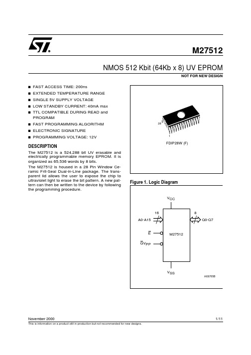
1/11NOT FOR NEW DESIGNNovember 2000This is information on a product still in production but not recommended for new designs.M27512NMOS 512 Kbit (64Kb x 8) UV EPROMs FAST ACCESS TIME: 200nss EXTENDED TEMPERATURE RANGE s SINGLE 5V SUPPLY VOLTAGE s LOW STANDBY CURRENT: 40mA max sTTL COMPATIBLE DURING READ and PROGRAMs FAST PROGRAMMING ALGORITHM s ELECTRONIC SIGNATURE sPROGRAMMING VOLTAGE: 12VDESCRIPTIONThe M27512 is a 524,288 bit UV erasable and electrically programmable memory EPROM. It is organized as 65,536 words by 8 bits.The M27512 is housed in a 28 Pin Window Ce-ramic Frit-Seal Dual-in-Line package. The trans-parent lid allows the user to expose the chip to ultraviolet light to erase the bit pattern. A new pat-tern can then be written to the device by following the programming procedure.Figure 1. Logic DiagramAI00765B16Q0-Q7V CCM27512GV PPV SS8A0-A15E 128FDIP28W (F)Figure 2. DIP Pin Connections permanent damage to the device. These are stress ratings only and operation of the device at these or any other conditions above those indicated in the Operating sections of this specification is not implied. Exposure to Absolute Maximum Rating conditions for extended periods may affect device reliability. Refer also to the STMicroelectronics SURE Program and other relevant quality document.Table 2. Absolute Maximum RatingsDEVICE OPERATIONThe six modes of operations of the M27512 are listed in the Operating Modes table. A single 5V power supply is required in the read mode. All inputs are TTL levels except for GV PP and 12V on A9 for Electronic Signature.Read ModeThe M27512 has two control functions, both of which must be logically active in order to obtain data at the outputs. Chip Enable (E) is the power control and should be used for device selection.Output Enable (G) is the output control and should be used to gate data to the output pins, inde-pendent of device selection. Assuming that the addresses are stable, address access time (t AVQV )is equal to the delay from E to output (t ELQV ). Data is available at the outputs after delay of t GLQV from the falling edge of G, assuming that E has been low and the addresses have been stable for at least t AVQV -t GLQV .Standby ModeThe M27512 has a standby mode which reduces the maximum active power current from 125mA to 40mA. The M27512 is placed in the standby mode by applying a TTL high signal to the E input. When in the standby mode, the outputs are in a high impedance state, independent of the GV PP input.Two Line Output ControlBecause EPROMs are usually used in larger mem-ory arrays, the product features a 2 line control function which accommodates the use of multiple memory connection. The two line control function allows :a. the lowest possible memory power dissipation,b. complete assurance that output bus contention will not occur.M275122/11For the most efficient use of these two control lines,E should be decoded and used as the primary device selecting function, while GV PP should be made a common connection to all devices in the array and connected to the READ line from the system control bus. This ensures that all dese-lected memory devices are in their low power standby mode and that the output pins are only active when data is required from a particular mem-ory device.System ConsiderationsThe power switching characteristics of fast EPROMs require careful decoupling of the devices.The supply current, I CC , has three segments that are of interest to the system designer : the standby current level, the active current level, and transient current peaks that are produced by the falling and rising edges of E. The magnitude of the transient current peaks is dependent on the capacitive and inductive loading of the device at the output. The associated transient voltage peaks can be sup-pressed by complying with the two line output control and by properly selected decoupling ca-pacitors. It is recommenced that a 1µF ceramic capacitor be used on every device between V CC and V SS . This should be a high frequency capacitor of low inherent inductance and should be placed as close to the device as possible. In addition, a 4.7µF bulk electrolytic capacitor should be used between V CC and V SS for every eight devices. The bulk capacitor should be located near the power supply connection point. The purpose of the bulk capacitor is to overcome the voltage drop caused by the inductive effects of PCB traces.ProgrammingWhen delivered, and after each erasure, all bits of the M27512 are in the “1" state. Data is introduced by selectively programming ”0s" into the desired bit locations. Although only “0s” will be programmed,both “1s” and “0s” can be present in the data word.The only way to change a “0" to a ”1" is by ultraviolet light erasure. The M27512 is in the programming mode when GV PP input is at 12.5V and E is at TTL-low. The data to be programmed is applied 8bits in parallel to the data output pins. The levels required for the address and data inputs are TTL.The M27512 can use PRESTO Programming Algo-rithm that drastically reduces the programming time (typically less than 50 seconds). Nevertheless to achieve compatibility with all programming equipment, the standard Fast Programming Algo-rithm may also be used.Fast Programming AlgorithmFast Programming Algorithm rapidly programs M27512 EPROMs using an efficient and reliable method suited to the production programming en-vironment. Programming reliability is also ensured as the incremental program margin of each byte is continually monitored to determine when it has been successfully programmed. A flowchart of the M27512 Fast Programming Algorithm is shown in Figure 8.Note: X = V IH or V IL , V ID = 12V ± 0.5%.Table 3. Operating ModesTable 4. Electronic SignatureDEVICE OPERATION (cont’d)M275123/11Figure 3. AC Testing Input Output WaveformsInput Rise and Fall Times ≤ 20ns Input Pulse Voltages0.45V to 2.4V Input and Output Timing Ref. Voltages0.8V to 2.0VAC MEASUREMENT CONDITIONSFigure 4. AC Testing Load CircuitNote that Output Hi-Z is defined as the point where datais no longer driven.Note: 1.Sampled only, not 100% tested.Table 5. Capacitance (1) (T A = 25 °C, f = 1 MHz )Figure 5. Read Mode AC WaveformsM275124/11Notes:1.V CC must be applied simultaneously with or before V PP and removed simultaneously or after V PP .2.Sampled only, not 100% tested.Table 7. Read Mode AC Characteristics (1)(T A = 0 to 70 °C or –40 to 85 °C; V CC = 5V ± 5% or 5V ± 10%; V PP = V CC)Note: 1.V CC must be applied simultaneously with or before V PP and removed simultaneously or after V PP .Table 6. Read Mode DC Characteristics (1)(T A = 0 to 70 °C or –40 to 85 °C; V CC = 5V ± 5% or 5V ± 10%; V PP = V CC )CC PP PP Table 8. Programming Mode DC Characteristics (1)(T A = 25 °C; V CC = 6.25V ± 0.25V; V PP = 12.75V ± 0.25V)M275125/11Notes. 1. V CC must be applied simultaneously with or before V PP and removed simultaneously or after V PP .2. The Initial Program Pulse width tolerance is 1 ms ± 5%.3. The length of the Over-program Pulse varies from 2.85 ms to 78.95 ms, depending on the multiplication value of the iteration counter.4. Sampled only, not 100% tested.Table 10. Programming Mode AC Characteristics (1)(T A = 25 °C; V CC = 6.25V ± 0.25V; V PP = 12.75V ±0.25V)CC PP PP Table 9. MARGIN MODE AC Characteristics (1)(T A = 25 °C; V CC = 6.25V ± 0.25V; V PP = 12.75V ± 0.25V)M275126/11M27512 Figure 6. MARGIN MODE AC WaveformFigure 7. Programming and Verify Modes AC Waveforms7/11Figure 8. Fast Programming FlowchartFigure 9. PRESTO Programming FlowchartDEVICE OPERATION (cont’d)The Fast Programming Algorithm utilizes two differ-ent pulse types : initial and overprogram. The du-ration of the initial E pulse(s) is 1ms, which will then be followed by a longer overprogram pulse of length 3ms by n (n is an iteration counter and is equal to the number of the initial one millisecond pulses applied to a particular M27512 location), before a correct verify occurs. Up to 25 one-millisecond pulses per byte are provided for before the over program pulse is applied.The entire sequence of program pulses is per-formed at V CC = 6V and GV PP = 12.5V (byte verifi-cations at V CC = 6V and GV PP = V IL ). When the Fast Programming cycle has been completed, all bytes should be compared to the original data with V CC = 5V.PRESTO Programming AlgorithmPRESTO Programming Algorithm allows to pro-gram the whole array with a guaranted margin, in a typical time of less than 50 seconds (to be com-pared with 283 seconds for the Fast algorithm).This can be achieved with the STMicroelectronics M27512 due to several design innovations de-scribed in the next paragraph that improves pro-gramming efficiency and brings adequate marginfor reliability. Before starting the programming the internal MARGIN MODE circuit is set in order to guarantee that each cell is programmed with enough margin.Then a sequence of 500µs program pulses are applied to each byte until a correct verify occurs.No overprogram pulses are applied since the verify in MARGIN MODE provides the necessary margin to each programmed cell.Program InhibitProgramming of multiple M27512s in parallel with different data is also easily accomplished. Except PP ) of the parallel M27512 may be common. A TTL low level pulse applied to a M27512’s E input, with GV pp at 12.5V,will program that M27512. A high level E input inhibits the other M27512s from being pro-grammed.Program VerifyA verify (read) should be performed on the pro-grammed bits to determine that they were correctly programmed. The verify is accomplished with GV pp IL . Data should be verified t DV after the falling edge of E.M275128/11Electronic SignatureThe Electronic Signature mode allows the reading out of a binary code from an EPROM that will identify its manufacturer and type. This mode is intended for use by programming equipment to automatically match the device to be programmed with its corresponding programming algorithm.This mode is functional in the 25 °C ± 5 °C ambient temperature range that is required when program-ming the M27512. To activate this mode, the pro-gramming equipment must force 11.5V to 12.5V on address line A9 of the M27512. Two identifier bytes may then be sequenced from the device outputs by toggling address line A0 from V IL to V IH . All other address lines must be held at V IL during Electronic Signature mode, except for A14 and A15 which should be high. Byte 0 (A0 = V IL ) represents the manufacturer code and byte 1 (A0 = V IH ) the device identifier code.ERASURE OPERATION (applies to UV EPROM)The erasure characteristic of the M27512 is such that erasure begins when the cells are exposed tolight with wavelengths shorter than approximately 4000 Å. It should be noted that sunlight and some type of fluorescent lamps have wavelengths in the 3000-4000 Å range. Research shows that constant exposure to room level fluorescent lighting could erase a typical M27512 in about 3 years, while it would take approximately 1 week to cause erasure when expose to direct sunlight. If the M27512 is to be exposed to these types of lighting conditions for extended periods of time, it is suggested that opaque labels be put over the M27512 window to prevent unintentional erasure. The recommended erasure procedure for the M27512 is exposure to short wave ultraviolet light which has wavelength 2537 Å.The integrated dose (i.e. UV intensity x exposure time) for erasure should be a minimum of 15W-sec/cm 2. The erasure time with this dosage is approximately 15 to 20 minutes using an ultraviolet lamp with 12000 µW/cm 2 power rating. The M27512 should be placed within 2.5 cm (1 inch) of the lamp tubes during the erasure. Some lamps have a filter on their tubes which should be re-moved before erasure.-2200 ns, 5V ±5% blank 250 ns, 5V ±5% -3300 ns, 5V ±5% -20200 ns, 5V ±10%-25250 ns, 5V ±10%FFDIP28W10 to 70 °C 6–40 to 85 °CORDERING INFORMATION SCHEMEFor a list of available options (Speed, V CC Tolerance, Package, etc) refer to the current Memory Shortform catalogue.For further inform ation o n any aspect of this device, please cont act STMicroelectronics Sales Office nearest to you.M275129/11M27512Drawing is not to scale 10/11元器件交易网M27512 Information furnished is believed to be accurate and reliable. However, STMicroelectronics assumes no responsibility for the consequencesof use of such information nor for any infringement of patents or other rights of third parties which may result from its use. No license is grantedby implication or otherwise under any patent or patent rights of STMicroelectronics. Specifications mentioned in this publication are subjectto change without notice. This publication supersedes and replaces all information previously supplied. STMicroelectronics products are notauthorized for use as critical components in life support devices or systems without express written approval of STMicroelectronics.The ST logo is registered trademark of STMicroelectronicsAll other names are the property of their respective owners© 2000 STMicroelectronics - All Rights ReservedSTMicroelectronics GROUP OF COMPANIESAustralia - Brazil - China - Finland - France - Germany - Hong Kong - India - Italy - Japan - Malaysia - Malta - Morocco -Singapore - Spain - Sweden - Switzerland - United Kingdom - U.S.A.11/11。
摩缇马帝multimatic底盘及调教简介
Objective Testing
Multimatic’s unique multi-post rig testing and vehicle characterisation techniques offer an easily interpreted objective-based methodology for assessing a vehicle’s ride and handling performance. Using in-house developed servo-hydraulic actuators in conjunction with a proprietary controller and software suite, a vehicle’s dynamic signature can be identified. The analysis returns data on the dynamic characteristics of the vehicle’s structure, suspension and tires as well as an overall assessment of performance.
Closed-Loop Vehicle Closed-Loop Vehicle Dynamics Optimisation Dynamics Optimization
Multimatic provides development and tuning services that integrate three crucial testing and evaluation disciplines into a “Closed-Loop Vehicle Dynamics Optimisation” process.
支付方式
支付方式Terms of PaymentAs we all know payment is the core of a contract in the international trade. Specific payment tools and payment methods are always negotiated between the two trading parties. There are three main tools: Bill of Exchange (draft)(汇票), Promissory Note(本票)and Check(支票). As to payment methods, remittance(汇付), collection(托收)and letter of credit (L/C)(信用证)are commonly used. Furthermore, most transactions are settled on L/C basis.(一) Tools of PaymentI. Bill of ExchangeA bill of exchange is an unconditional order in writing signed by the person (drawer) such as a buyer, and addressed to another person (drawee), typically a bank, requiring the drawee to pay a stated sum of money to another person (payee), often a seller, on demand or at a fixed future time.Exchange for USD25,000.00No. CI-00888March 15 20 09 AT SIGHT of this First of Exchange (Second Unpaid)Pay to the order of UVW ExportsThs sum of Twenty Five Thousand US DollarsDrawn under documentary credit No. SB-87654 of The Sun Bank,Sunlight City, Import-country, dated January 26, 2009To The Moon Bank UVW Exports5 Moonlight Blvd.Export-city and Postal Code, Export-Country ________________This sample bill of exchange is drawn on The Moon Bank by the UVW Exports.A bill of exchange must fulfill the following requirements:1. the word “exchange” or “draft”.2. an unconditional order in writing.3. name and address of the drawee.4. drawer’s signature, usually seller’s signature.5. date and place of issue.6. name of the payee, usually the seller or its nominated bank.7. tenor.8. place of payment.9. Amount.Types of bill of exchange(1)Sight Draft/ Term Draft(即期和远期汇票)The sight draft is most commonly used in international trade. In a sight draft, the payment is on demand or on presentation of the negotiation documents to the paying bank or the importer.The term draft, also called time draft or usance draft, is used in a deferred(延期)payment arrangement. The payment is on the maturity date determinable in accordance with the stipulations of the Letter of Credit. The maturity date can be ata stated period at sight or after date.For example:at 90 days sight;at 180 days after date;at 150 days after B/L dateWhen the drawee accepts a time draft, he will write or stamp the word “ACCEPTED”。
27128(128K-EPROM)
Figure 1. Logic DiagramM27128ANMOS 128K (16K x 8) UV EPROMFAST ACCESS TIME: 200nsEXTENDED TEMPERATURE RANGE SINGLE 5 V SUPPLY VOLTAGE LOW STANDBY CURRENT: 40mA max TTL COMPATIBLE DURING READ and PROGRAMFAST PROGRAMMING ALGORITHM ELECTRONIC SIGNATURE PROGRAMMING VOLTAGE: 12VDESCRIPTIONThe M27128A is a 131,072 bit UV erasable and electrically programmable memory EPROM. It is organized as 16,384 words by 8 bits.The M27128A is housed in a 28 Pin Window Ce-ramic Frit-Seal Dual-in-Line package. The trans-parent lid allows the user to expose the chip to ultraviolet light to erase the bit pattern. A new pattern can then be written to the device by follow-ing the programming procedure.Table 1. Signal NamesMarch 19951/10Figure 2. DIP Pin ConnectionsNote: Except for the rating "Operating Temperature Range", stresses above those listed in the Table "Absolute Maximum Ratings" may cause permanent damage to the device. These are stress ratings only and operation of the device at these or any other conditions above those indicated in the Operating sections of this specification is not implied. Exposure to Absolute Maximum Rating conditions for extended periods may affect device reliability. Refer also to the SGS-THOMSON SURE Program and other relevant quality documents.Table 2. Absolute Maximum RatingsDEVICE OPERATIONThe seven modes of operation of the M27128A are listed in the Operating Modes table. A single 5V power supply is required in the read mode. All inputs are TTL levels except for V PP and 12V on A9for Electronic Signature.Read ModeThe M27128A has two control functions, both of which must be logically satisfied in order to obtain data at the outputs. Chip Enable (E) is the power control and should be used for device selection.Output Enable (G) is the output control and should be used to gate data to the output pins, inde-pendent of device selection.Assuming that the addresses are stable, address access time (t AVQV ) is equal to the delay from E to output (t ELQV ). Data is available at the outputs after the falling edge of G, assuming that E has been low and the addresses have been stable for at least t AVQV -t GLQV .Standby ModeThe M27128A has a standby mode which reduces the maximum active power current from 85mA to 40mA. The M27128A is placed in the standby mode by applying a TTL high signal to the E input. When in the standby mode, the outputs are in a high impedance state, independent of the G input.Two Line Output ControlBecause EPROMs are usually used in larger mem-ory arrays, this product features a 2 line control function which accommodates the use of multiple memory connection. The two line control function allows:a. the lowest possible memory power dissipation,b. complete assurance that output bus contention will not occur.For the most efficient use of these two control lines,E should be decoded and used as the primary device selecting function, while G should be made a common connection to all devices in the array and connected to the READ line from the system control bus.This ensures that all deselected memory devices are in their low power standby mode and that the output pins are only active when data is required from a particular memory device.System ConsiderationsThe power switching characteristics of fast EPROMs require careful decoupling of the devices.The supply current, I CC , has three segments that are of interest to the system designer: the standby current level, the active current level, and transient current peaks that are produced by the falling and rising edges of E. The magnitude of this transient current peaks is dependent on the capacitive and inductive loading of the device at the output. The associated transient voltage peaks can be sup-pressed by complying with the two line output control and by properly selected decoupling ca-pacitors. It is recommended that a 1µF ceramic capacitor be used on every device between V CC and V SS . This should be a high frequency capacitorof low inherent inductance and should be placed as close to the device as possible. In addition, a 4.7µF bulk electrolytic capacitor should be used between V CC and GND for every eight devices. The bulk capacitor should be located near the power supply connection point. The purpose of the bulk capacitor is to overcome the voltage drop caused by the inductive effects of PCB traces.ProgrammingWhen delivered (and after each erasure for UV EPPROM), all bits of the M27128A are in the “1"state. Data is introduced by selectively program-ming ”0s" into the desired bit locations. Although only “0s” will be programmed, both “1s” and “0s”can be present in the data word. The only way to change a “0" to a ”1" is by ultraviolet light erasure.The M27128A is in the programming mode when V PP input is at 12.5V and E and P are at TTL low.The data to be programmed is applied 8 bits in parallel, to the data output pins. The levels required for the address and data inputs are TTL.Fast Programming AlgorithmFast Programming Algorithm rapidly programs M27128A EPROMs using an efficient and reliable method suited to the production programming en-vironment. Programming reliability is also ensured as the incremental program margin of each byte isIH IL IDTable 3. Operating ModesTable 4. Electronic SignatureDEVICE OPERATION (cont’d)Figure 3. AC Testing Input Output WaveformsInput Rise and Fall Times ≤ 20ns Input Pulse Voltages0.45V to 2.4V Input and Output Timing Ref. Voltages0.8V to 2.0VAC MEASUREMENT CONDITIONSFigure 4. AC Testing Load CircuitNote that Output Hi-Z is defined as the point where datais no longer driven.Note: 1.Sampled only, not 100% tested.Table 5. Capacitance (1) (T A = 25 °C, f = 1 MHz )Figure 5. Read Mode AC WaveformsNotes:1.V CC must be applied simultaneously with or before V PP and removed simultaneously or after V PP .2.Sampled only, not 100% tested.Table 7. Read Mode AC Characteristics (1)(T A = 0 to 70 °C or –40 to 85 °C; V CC = 5V ± 5% or 5V± 10%; V PP = V CC )CC PP PP Table 6. Read Mode DC Characteristics (1)(T A = 0 to 70 °C or –40 to 85 °C; V CC = 5V ± 5% or 5V ± 10%; V PP = V CC )Note: 1. V CC must be applied simultaneously with or before V PP and removed simultaneously or after V PP .Table 8. Programming Mode DC Characteristics (1)(T A = 25 °C; V CC = 6V ± 0.25V; V PP = 12.5V ±0.3V)Notes: 1.V CC must be applied simultaneously with or before V PP and removed simultaneously or after V PP . 2.The Initial Program Pulse width tolerance is 1 ms ± 5%.3.The length of the Over-program Pulse varies from 2.85 ms to 78.95 ms, depending on the multiplication value of the iteration counter.4.Sampled only, not 100% tested.Table 9. Programming Mode AC Characteristics (1)(T A = 25 °C; V CC = 6V ± 0.25V; V PP = 12.5V ± 0.3V)Figure 6. Programming and Verify Modes AC WaveformsFigure 7. Programming Flowchart continually monitored to determine when it has been successfully programmed. A flowchart of the M27128A Fast Programming Algorithm is shown on the last page. The Fast Programming Algorithm utilizes two different pulse types: initial and over-program.The duration of the initial P pulse(s) is 1ms, which will then be followed by a longer overprogram pulse of length 3ms by n (n is equal to the number of the initial one millisecond pulses applied to a particular M27128A location), before a correct verify occurs.Up to 25 one-millisecond pulses per byte are pro-vided for before the over program pulse is applied.The entire sequence of program pulses and byte verifications is performed at V CC = 6V and V PP =12.5V. When the Fast Programming cycle has been completed, all bytes should be compared to the original data with V CC = 5 and V PP = 5V.Program InhibitProgramming of multiple M27128A’s in parallel with different data is also easily accomplished. Except for E, all like inputs (including G) of the parallel M27128A may be common. A TTL low pulse ap-plied to a M27128A’s E input, with V PP = 12.5V, will program that M27128A. A high level E input inhibits the other M27128As from being programmed.DEVICE OPERATION (cont’d)Program VerifyA verify should be performed on the programmed bits to determine that they were correctly pro-grammed. The verify is accomplished with G = V IL ,E = V IL , P = V IH and V PP at 12.5V.Electronic SignatureThe Electronic Signature mode allows the reading out of a binary code from an EPROM that will identify its manufacturer and type. This mode is intended for use by programming equipment to automatically match the device to be programmed with its corresponding programming algorithm.This mode is functional in the25°C ± 5°C ambient temperature range that is required when program-ming the M27128A.T o activate this mode, the programming equipment must force 11.5V to 12.5V on address line A9 of the M27128A. Two identifier bytes may then be se-quenced from the device outputs by toggling ad-dress line A0 from V IL to V IH . All other address lines must be held at V IL during Electronic Signature mode. Byte 0 (A0 = V IL ) represents the manufac-turer code and byte 1 (A0 = V IH ) the device identifier code. For the SGS-THOMSON M27128A, these two identifier bytes are given below.ERASURE OPERATION (applies to UV EPROM)The erasure characteristic of the M27128A is such that erasure begins when the cells are exposed to light with wavelengths shorter than approximately 4000 Å. It should be noted that sunlight and some type of fluorescent lamps have wavelengths in the 3000-4000 Å range. Research shows that constant exposure to room level fluorescent lighting could erase a typical M27128A in about 3 years, while it would take approximately 1 week to cause erasure when exposed to direct sunlight. If the M27128A is to be exposed to these types of lighting conditions for extended periods of time, it is suggested that opaque labels be put over the M27128A window to prevent unintentional erasure. The recommended erasure procedure for the M27128A is exposure to short wave ultraviolet light which has wavelength 2537 Å. The integrated dose (i.e. UV intensity x exposure time) for erasure should be a minimum of 15 W-sec/cm 2. The erasure time with this dosage is approximately 15 to 20 minutes using an ultra-violet lamp with 12000 µW/cm 2 power rating. The M27128A should be placed within 2.5cm (1 inch)of the lamp tubes during the erasure. Some lamps have a filter on their tubes which should be re-moved before erasure.-2200 ns, 5V ±5% blank 250 ns, 5V ± 5%-3300 ns, 5V ± 5% -4450 ns, 5V ± 5% -20200 ns, 5V ± 10%-25250 ns, 5V ± 10%-30300 ns, 5V ± 10%FFDIP28W10 to 70 °C 6–40 to 85 °CORDERING INFORMATION SCHEMEFor a list of available options (Speed, V CC Tolerance, Package, etc...) refer to the current Memory Shortform catalogue.For further information on any aspect of this device, please contact SGS-THOMSON Sales Office nearest to you.Drawing is not to scaleInformation furnished is believed to be accurate and reliable. However, SGS-THOMSON Microelectronics assumes no responsibility for the consequences of use of such information nor for any infringement of patents or other rights of third parties which may result from its use. No license is granted by implication or otherwise under any patent or patent rights of SGS-THOMSON Microelectronics. Specifications mentioned in this publication are subject to change without notice. This publication supersedes and replaces all information previously supplied. SGS-THOMSON Microelectronics products are not authorized for use as critical components in life support devices or systems without express written approval of SGS-THOMSON Microelectronics.© 1995 SGS-THOMSON Microelectronics - All Rights ReservedSGS-THOMSON Microelectronics GROUP OF COMPANIESAustralia - Brazil - France - Germany - Hong Kong - Italy - Japan - Korea - Malaysia - Malta - Morocco - The Netherlands -Singapore - Spain - Sweden - Switzerland - Taiwan - Thailand - United Kingdom - U.S.A.。
科巴9550用户手册说明书
............................Attach cups to bracket.Attach detector to bracket.Plug power cord into detector.Attach bracket to windshield.Bend bracket for correct detection angle (if needed).Do not use the ESD-9550 to bend bracket.Plug power cord i n to cigare t t e lighte r .LocationSe l e c ting the pro p er location to mount the Co b r a ESD-9550 is ve r y impo r t a n t for optimum pe r fo r m a n c e.Both radar and laser tra n s m i s s i o n s pass through glass but not through other object s .For this reason the Co b r a ESD-9550 lenses must not be bloc k e d .The Laser Eye should have a view of the rear window to take adva n tage of its 360˚ d e t e c t i o n ca p a b i l i t y.It is best to locate your d e t e c tor as low on the fro n t windshield as po s s i b l e .Examples of metal in the windshield area that can block or weaken incoming radar/laser signals:1.Windshield wiper blades.2.Mirrored sun screens.3.Regular tinted glass does not affect radar reception,although the darker tint at the top of the tinted windshield prevents laser light from penetrating.4.Heated windshields,currently available as an option for some Ford® (Instaclear) and GM®(Electriclear vehicles act as an impenetrable barrier to radar signals).If in doubt,check with your dealer to see if this applies to your vehicle.Windshield MountingLocationWindshield MountingPlug power cord into detector.Plug power cord i n to cigare t t e lighte r .Peel protective paper off one side of hook and loop material.Place on dash.Peel top paper off.Place detector on hook and loop pad.123456Rotate ON-OFF Volume Control to left (away from you).An audible “tone”will indicate the unit is on.The unit will perform a self-test and the following message will appear …Testing…System Ready.1NoteFor your convenienceDisplay Dim,City/Highway,and Muting mode settings are retained in memory even when the power is unplugged.NoteThe ESD-9550 will retain the chosen mode while OFF.Press and releaseDim button once to select normal setting.Press and release Dim button a second timeto select Dim setting.Press and releaseDim button a third time to select Dimmer setting.Press and release Dim button again to select Dark setting.1LED DisplaysNoteA four position Dim mode is provided for dusk or night driving (please see Dim Button,page 10 for details).For more detailed operation instructions on display brightness,see page 10.For more detailed operation instructions on set highway/city mode,see page 11.Highway ModePress and release City button again.HWY will be displayed for 2 seconds followed by h .A double beep confirms highway mode.Press and release City button.CTY will display while in City mode and remain on for 2 seconds.1Manual MutingPress and release Mute button to reduce volume while signal is in progress.MUTE will appear in the display.To Switch Between ModesPress and release Mute Button when no signal is being received.111Plug power cord into detector.Plug power cord i n to cigare t t e lighte r .2Rotate ON-OFF Volume Control to the left(away from you).13For more detailed operation instructions on setting muting mode,see page 13.The message “Testing…System Ready “ will be displayed,along with 3 beeps.The Compass directions will then be displayed.Highway/City ModeThe Highway/City function is controlled by a 2-s t ep butto n .To select City Mode:Press and release City button and CTY will be displayed for 2 seconds followed by c .A single beep confirms City mode.1x ContinuedPress and re l e a s e Mute b u t t on when no signal is being re c e i v e d .1Manual Muting of the AudioUse this operation to turn off the audio alarm atany time.Highway/City ModeTo select Highway Mode:Press and release Ci t y butto n .HWY will be displayed for 2 seconds followed by h.Highway/City Modex ContinuedNoteTo completely turn off incoming alerts while in auto mode,press and release mute button.NoteMute=“Beep”ORAuto Mute=“Beep-Beep”The message “Drive in 2 circles…press City when done.”will then be displayed. Drive your car in a circle twice and then press City.Your compass will be set.The display provides 8 primary directions;N,NE,E,SE,S, SW,W and NW.NoteYour compass may not give a correct reading if you are inside any enclosure, building or close to a large metal tractor trailer,truck or train.Your compass will work again correctly as soon as you get away from these locations.There is no need to calibrate yourcompass again.Press City button for a minimum of2 pass is displayed.NotePushing City button formore than 2 secondsproduces a single beepconfirmation tone.NoteIf you decide to re-locateyour ESD-9550 to a differentlocation in your vehicle ormove it to another vehicle,itis best to recalibrate thecompass.12Selecting Manual Muting ModeIn Manual Mute mode the alerts will always beheard at the set volume level.Press and release Mute Button when nosignal is being received.M u t e will appear onthe display for 2 seconds,then disappear.1Auto Mute will appear in display for 2 seco n ds,then disappear.All future alarms will be Au t o Mu t e.MutingVG-2 AlertX, K, Ka AlertVG-2 UndetectableThe Co b r a ESD-9550 is undete c table by po l i c e VG -2d e t e c tion dev i c e s .It will alert you when one is in use near your ve h i c l e .Du r ing this time,the unit is still on full alert and able to dete ct other signals.VG-2on the front of the unit will be displayed.NoteThe display does not indicate signal strength.Weakest signalStrongest signalInstant-On DetectionThe Cobra ESD-9550 is also designed to detect Instant-on speed monitoring signals.Immediate action is required when warning is given.Audible Alarm SpeakerA different alert tone will sound for X,K,Ka,Laser (a distinctly different tone for each of the three laser signals:LTI 20-20,UltraLyte and ProLaser),VG-2,and Safety and Strobe Alert signals.Audible AlarmSpeakerBandDetectionBand DetectionThis dete c tor is designed to dete c t X,K ,S u p e r wide Ka Band Ra d a r ,Laser (including LT I 2 0-20*,U l t r a Ly t e* and ProLaser* te c h n o l o g i e s ),VG -2,Sa f e t y Al e r t and St r o b e Al e r t* signals.* 360˚ De t e c t i o nLaser will be displayed followed by a scrolling message of “UltraLyte”,“ProLaser”or “20/20”depending on signal received.Safety Alert® Traffic Warning System and Strobe Alert ™Safety Alert® Traffic Warning System and Strobe Alert™ will alert you with the following warnings:Emergency Vehicle,Road Hazard and Train.“Emergency Vehicle”will be displayed as scrolling message.“Road Hazard”will be displayed.“Train”will be displayed.Safety Alert ®Tr a f f i c W a r n i n g System andStrobe Alert™Strobe Alert ™Safety Alert®“Emergency Vehicle”will be displayed as scrollingmessage.LIDARs must have a clearline of sight to target avehicle during the entiremeasurement interval.Intervening objects such assignposts,utility poles,treebranches,etc.,will preventa valid speed reading.420-080-N-001St r a i g h t 12V Power Co r d $10.00420-080-N -002Cu r led 12V Power Co r d $10.00545-139-N -001Windshield Mo u n ting Bra c k e t $7.00Item #Description Cost Ea.Qty.AmountPlease print clearlyNameAddress (No P.O .Box)City StateZipTelephone ( )Credit Card No.Exp.DateCustomer SignatureCircle One:Visa MasterCard Discover Allow 4 to 6 weeks for delivery.Offer valid in Continental U.S.only.For credit card orders fill out order formand fax to:1.773.622.2269or call 1.773.889.3087(Press 1 from the main menu)8:00 am - 8:00 pm,M-F,CST.Ma k e check or money order (no stamps)payable to:Cobra Electronics 6500 West Co r tland St .Ch i c a g o ,IL 60707At t n :Accessories Dept.DontNeed ThisPageM icrRadar/Laser Detector With Electronic Digital Compass *O p e r ating Instru c tions for your Co b r a9 Band ESD 9550© 2000 Cobra Electronics Corp.Printed in ThailandPart No. 480-299-P-001If you think you need service call 1.773.889.3087“If your product should require factory service please call Cobra first before sending your unit in.This will ensure the fastest turn-around time on your repair.”You may be asked to send your unit to the Cobra factory.It will be necessary to furnish the following in order to have the product serviced and returned.1.For Warranty Repair include some form of pr oof-of-purchase,such as a mechanical reproduction or carbon or a sales receipt.If you send the original receipt it cannot be returned.2.Send the entire product.3.Enclose a description of what is happening with the unit.Include a typed or clearly print name and address of where the unit is to be returned.4.Pack unit securely to prevent damage in transit.If possible,use the original packing material.5.Ship prepaid and insured by way of a traceable carrier such as United Parcel Service (UPS) or First Class Mail to:Cobra Factory Service,Cobra Electronics Corporation,6500 W.Cortland St.,Chicago,IL 60707.6.If the unit is in war ranty,upon receipt of your unit it will either be repaired or exchanged depending on the model.Please allow approximately 3 to 4 weeks before contacting us for status.If the unit is out of warranty a letter will automatically be sent informing you of the repair charge or replacement charge.If you have any questions,please call 1.773.889.3087 for assistance.If You Think You Need Service and Strobe Alert™Use of this product is not intend-ed to,and does not,ensure that the motorist and any passenger will not be involved in a traffic accident.It is only intended to alert the motorist that an emer-gency or service vehicle equipped with a CODE 3,Strobe (Opticom*or Tomar Preemption System) or Cobra Safety Alert Transmitter is in the area as defined by the range of the product.Please call your local Fire/Police department to verify if coverage exists in your area.Motorists are expected to exercise all due caution while using this product,and to ob-serve and follow all applicable traffic laws.Operators of emergency or service vehicles are also expected to exercise all due caution while using this product,and to observe and follow all applicable traffic laws.*Opticom is a registered trademark of 3M Corporation Nothing comes close to a Co b r a ™© 2000 Cobra Electronics Corporation6500 West Cortland StreetChicago, IL 60707Thank you for purchasing the Cobra ESD-9550 Radar/Laser Detector.Properly used,this Cobra product will give you many years of reliable service.Customer Support Should you encounter any problems with the product or not understand its many features,please refer to this owner’s manual.If,after referring to the manual,you still need help,call Cobra Customer Service at 773.889.3087.1.On/Off Volume ControlMute ButtonDim ButtonAudio Alerts SpeakerHighway/City ButtonBand/Signal Strength/Compass DirectionIndicatorsLaser EyeWindshield BracketMount12V DC Power JackAudio JackThe C o b r a line of quality prod u c ts also includes:•Ci t i z ens Band Ra d i o s •Mi c r o T a l k ™Ra d i o s •Ac c e s s o r i e s •Sa f e t y A l e r t ™Traffic Wa r ning Sys t e m sNothing comes close to a Co b r a ™。
- 1、下载文档前请自行甄别文档内容的完整性,平台不提供额外的编辑、内容补充、找答案等附加服务。
- 2、"仅部分预览"的文档,不可在线预览部分如存在完整性等问题,可反馈申请退款(可完整预览的文档不适用该条件!)。
- 3、如文档侵犯您的权益,请联系客服反馈,我们会尽快为您处理(人工客服工作时间:9:00-18:30)。
arXiv:astro-ph/0011411v1 22 Nov 20001SIGNATUREOFTHESOLARCYCLEINTHELOWDEGREEP-MODESUSINGMARK-ISebasti´anJ.Jim´enez-Reyes1,2,ThierryCorbard1,andPereL.Pall´e21HighAltitudeObservatory,NCAR,POBox3000,Boulder,CO80307USA
2InstitutodeAstrof´ısicadeCanarias,E-38701,LaLaguna,Tenerife,Spain
ABSTRACTHighqualityobservationsofthelowdegreep-modesex-istforalmosttwocompletesolarcyclesusingthesolarspectrophotometerMark-I,locatedandoperatingattheObservatoriodelTeide(Tenerife,Spain).Inthiswork,theobservationsavailablehavebeenre-analyzedoveramuchwidertimeintervalthanbefore.Weanalyzethetimevariationoftheyearlyfrequencyshiftanditsfre-quencydependence.Thisinformationwillbeusedinordertoaverageannualpowerspectrabyremovingtheeffectofthesolarcycle.Usingthisaveragepowerspec-trum,anewestimateoftherotationalsplittingsisat-tempted.1.INTRODUCTIONUnderstandingthewellknownsolarvariabilityisoneofthemajorgoalsofsolarphysics.Inthelastyears,thehe-lioseismicdata,bymeansofthefrequencyshiftsofsolarp-modes,havedemonstratedtobeverysensitivetothesolaractivitycycle.Inparticular,theexistenceofaposi-tiveshiftof∼0.4µHz,peak-to-peak,withthesolarcycleisverywellknown(R´eguloetal.1994,Jim´enez-Reyesetal.1998).ThespectrophotomerMark-I,hasbeencollectingsolarobservationsforalmosttwocompletesolarcycles.Theavailabledatabase,oneofthelongestforlowdegrees,couldbeusedtomeasurethemodeparameters.However,thevariationofthecentralfrequencyisanimportantef-fectwhichshouldbetakenintoaccountinordertouselongtimeseries.Inthiswork,wehaveanalyzedthetimevariationofthefrequencyshiftanditsfrequencydependence.Usingthisinformationweareabletoaveragetheannualspectrawhichisthenfittedinordertomeasurethemodeparam-eters,speciallytherotationalsplittings.2.ANALYSISOFTHEANNUALTIMESERIESThedatausedinthisworkcomefromtheobservationscarriedoutattheObservatoriodelTeideforabout15years,from1984to1999.TheobservationsconsistofdailymeasurementsofthesolarradialvelocityobtainedwiththeMark-Iresonantscatteringspectrometer.Briefly,aftercalibrationanddetrending,dailyvelocityresidualswerejoinedinconsecutive360daysleadingtoatotalof30timeserieswith6monthsincommonbetweencon-secutiveseries.Thecorrespondingpowerspectrawerecalculatedforeachoneofthetimeseries.
Figure1.Timevariationofthefrequencyshiftforlowdegree.
Inordertodeterminethefrequencyshift,allthepowerspectrahavebeencross-correlatedusingthesameref-erence.Thepositionofthemainpeakcanbemea-suredindifferentways.Here,weusethefactthatthecross-correlationbetweenLorentzianprofilesisanotherLorentzianprofilewhichcanbeusedtocalculatethecen-tralfrequencybyaleastsquaresminimization.
Thelowdegreemodesareasymptoticallyequalspacedinfrequency.Thiscanbeusedtosplitintwotheoriginalspectrum,onecontainingonlypeakswithevendegreesandtheothercontainingonlypeakscorrespondingtoodddegrees.Then,thesameprocedureasexplainedabove2Figure2.Timevariationofthetotalvelocitypowerdefinedastheareaunderthemainpeakofthecross-correlationfunction.
IntheFigure1weshowtheintegratedfrequencyshiftbetween2.5and3.7mHz.Theresultscorrespondingtoℓ=0,2andℓ=1,3havebeenplottedinthesubplotatthetop-rightcorneranditsaveraged(shifted-0.1µHz)isshowninthemainfigure,whichagreesverywellwiththeintegratedsignal.Theamplitude,peak-to-peak,ofthischangesisaround0.4µHz,asweexpected.
Thebestfitoftheannualradiofluxhasalsobeenplot-tedtoshowthegoodcorrelationbetweenthesolaractiv-ityandthefrequencyshift.Usingannualtimeserieswehavereducedthehighfrequencysignalinthevariationofthefrequencyshift,keepingthelongtermbehavior.Thus,thecorrelationlevelsbetweentheseparametersareclearlycloseto1.
Wehavealsocalculatedthetotalvelocitypowerde-finedhereastheareaunderthemainpeakofthecross-correlationfunction.OncethemainpeakisfittedasaLorentzianprofile,theareacanbecalculatedfromtheamplitudeandlinewidth.
Thefirstdemonstrationofthevariationforthevelocitypowerforallmeasuredp-modeswiththesolaractivitywasreportedbyPall´eetal.(1990)whereanincreaseof30to40%,anti-correlatedwiththesolaractivitycycle,wasfound.Afterwards,Angueraetal.(1992)foundsim-ilarresultsfollowingdifferenttechniques.Thoseresultswereinterpretedintermsofachangeintheefficiencyoftheexcitationofsuchmodes.Otherpossibilityshouldbetheabsorptionofmodepowerbymagneticstructureslikesunspots,activeregions,etc.Howevertheyrepresentasmallinfluenceanditcannotexplaintotallysuchhighra-tio.
IntheFigure2,wepresentthetimevariationoftheto-talvelocitypower.Again,weshowtheradiofluxscaledwhichdenotesherethebehaviorofthesolaractivitycy-cle.Fromthefigure,weareabletoseethevariationbetweenminimumandmaximumofthesolarcycleisaround35%whichagreeswithpreviousresults.More-over,itisclearthehighanti-correlationwiththesolar