A Linearization Technique for CMOS RF Power Amplifiers
射频学习参考书

射频学习参考书微波振荡器设计经典英文原版书籍五本1. RF and Microwave Oscillator DesignMichal Odyniec, Artech House, Inc. 20022. Oscillator Design and Computer SimulationRandall W. Rhea, Noble Publishing Corporation, 19953. Crystal Oscillator Circuits, Revised EditionRobert J. Matthys, Krieger Publishing Company, 19924. Crystal Oscillator Design and Temperature CompensationMarvin E. Frerking, Litton Educational Publishing, 19785. Fundamentals of RF Circuit Design with Low Noise OscillatorsJeremy Everard, John Wiley & Sons Ltd, 2001经典中文书籍三本1. 《微波振荡源》陈为怀、李玉梅著,2. 《微波固态振荡原理》潘儒沧、刁育才著,3. 《介质谐振器微波电路》4. 《S参数设计放大器和振荡器》设计实例和设计讲义1. 使用ADS设计VCO讲义2. VCO Design using Ansoft Designer3. Oscillator Basics and Low-Noise Techniques for Microwave Oscillators and VCOs4. Oscillator Phase Noise: A Tutorial5. 东南大学振荡器讲义6. 高頻振盪器之簡介滤波器设计经典中文书籍三本:1. 《微带电路》,清华大学《微带电路》编写组,人民邮电出版社,19792. 《现代微波滤波器的结构与设计》上册,甘本袚、吴万春著,科学出版社,19733. 《现代微波滤波器的结构与设计》下册,甘本袚、吴万春著,科学出版社,1973经典英文原版书籍三本:1. HF Filter Design and Computer SimulationRandall W. Rhea, Noble Publishing Corporation, 19942. Microstrip Filters for RF/Microwave ApplicationsJia-Sheng Hong, M. J. Lancaster, John Wiley & Sons Inc. 20013. Microwave Filters, Impedance Matching networks and Coupling StructuresGeorge L. Matthaei, Leo Young, E. M. T. Jones, Artech House, INC. 1980设计实例:1. ADS2003C关于微波滤波器设计和制作实例(中文56页)2. Ansoft Designer 关于微波滤波器设计和制作实例(英文43页)3. 微带抽头线发夹型滤波器设计4. Practical T echniques for Designing Microstrip Tapped Hairpin Filters on FR4 Laminates5. Design of Band Pass Filters With Ansoft HFSS and Serenade6. 浙大微波滤波器设计讲义微波功率放大器 ( PA ) 设计经典英文原版书籍八本1. Advanced Techniques in RF Power Amplifier DesignSteve C. Cripps, ARTECH HOUSE, INC. 20022. Radio Frequency Transistors and Practical Applications, Second EditionNorman Dye, Helge Granberg, Newnes, 20013. Feedback Linearization of RF Power AmplifiersJOEL L. DAWSON, THOMAS H. 4. LEE, KLUWER ACADEMIC PUBLISHERS, 20044. High Linearity RF Amplifier DesignPeter B. Kenington, ARTECH HOUSE, INC. 20005. RF Power Amplifier for Wireless CommunicationsSteve C. Cripps, ARTECH HOUSE, INC. 19996. RF Power AmplifiersMihai Albulet, Noble Publishing Corporation, 20017. Distortion in RF Power AmplifiersJoel Vuolevi, Timo Rahkonen, Artech House, Inc. 20038. Microwave Engineering, second editionDavid M. Pozar, JOHN WILEY & SONS, INC.,1998设计讲义:1. 清华大学功放设计讲义2. 东南大学功放设计讲义3. 浙江大学功放设计讲义4. MESFET 功率放大器设计:小信号法。
PA44
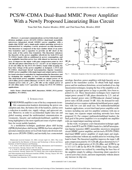
PCS/W-CDMA Dual-Band MMIC Power Amplifier With a Newly Proposed Linearizing Bias CircuitYoun Sub Noh ,Student Member,IEEE,and Chul Soon Park ,Member,IEEEAbstract—A personal communications service/wide-band code division multiple access (PCS/W-CDMA)dual-band monolithic microwave integrated circuit (MMIC)power amplifier with a single-chip MMIC and a single-path output matching network is demonstrated by adopting a newly proposed on-chip linearizer.The linearizer is composed of the base–emitter diode of an active bias transistor and a capacitor to provide an RF short at the base node of the active bias transistor.The linearizer enhances the linearity of the power amplifier effectively for both PCS and W-CDMA bands with no additional dc power consumption,and has negligible insertion power loss with almost no increase in die area.It improves the input 1-dB gain compression point by 18.5(20)dB and phase distortion by6.1)at an output power of 28(28)dBm for the PCS (W-CDMA)band while keeping the base bias voltage of the power amplifier as designed.A PCS and W-CDMA dual-band InGaP heterojunction bipolar transistor MMIC power amplifier with single input and output and no switch for band selection is embodied by implementing the linearizer and by designing the amplifier to have broad-band characteristics.The dual-band power amplifier exhibits an output power of 30(28.5)dBm,power-added efficiency of 39.5%(36%),and adjacent channel power ratio of 50)dBc at the output power of 28(28)dBm under 3.4-V operation voltage for PCS (W-CDMA)applications.Index Terms—Dual band,HBT,linearizer,MMIC,PCS,power amplifiers,W-CDMA.I.I NTRODUCTIONTHE POWER amplifier is one of the key components in mo-bile communication handsets determining the power con-sumption and,thus,the battery life of the handsets,and has seen a reduction in module size,supply voltage,and quiescent cur-rent.Moreover,in order to accommodate higher data rate and global roaming around the multistandard communication en-vironments,linearity and multimode/multiband capability are being highlighted as the most significant issues of power ampli-fiers for recent mobile handsets.As a modulation technique,quadrature phase shift keying (QPSK)/hybrid phase shift keying (HPSK)has been adopted for personal communications service/wide-band code division mul-tiple access (PCS/W-CDMA)and inevitably has a nonconstantManuscript received January 29,2002;revised April 22,2002.This work was supported by the Ministry of Science and Technology of Korea and Korea Institute of S&T Evaluation and Planning.Y .S.Noh is with the School of Engineering,Information and Communica-tions University,Yusong,Taejon 305-732,Korea.C.S.Park is with the School of Engineering,Information and Communica-tions University,Yusong,Taejon 305-732,Korea.He is also with the Electronics and Telecommunications Research Institute (ETRI),Yusong,Taejon 305-350,Korea (email:parkcs@icu.ac.kr).Publisher Item Identifier10.1109/JSSC.2002.801169.Fig.1.Schematic diagram of the two-stage dual-band power amplifier.envelope,therefore,power amplifiers with high linearity are re-quired in the transmitter system.To obtain both high output power and low nonlinear distortions,several methods of on-chip linearization techniques,keeping the bias of the amplifier as de-signed up to an input power as large as possible,have been re-ported [1],[2].These linearization techniques have improved output power around 0.5dB,phase distortion by 2.2Fig.2.Simulated VVFig.4.Simulated output power and adjacent channel power ratio of the two-stage power amplifier.Fig.5.Simplified block diagram of the two-stage PCS/W-CDMA dual-band power amplifier.(W-CDMA)band.With the capacitor,the maximum output power of10.7(12.8)dBm and ACPR up to15.3(15.7)dB at the input power ofless thanmore closely at the W-CDMA band because the transistor gain decreases as the frequency increases.The InGaP–GaAs HBT MMIC power amplifier was demon-strated using multiple fingers of a unit transistor of60(emitter area:2880for the power stage and720for thedriver stage).The fabricated MMIC power amplifier is shown in Fig.6.The total chip size of the MMIC is as small as840mFig.8.Measured ACPR of the two-stage PCS/W-CDMA dual-band power amplifier.TABLE IM EASURED P ERFORMANCES OF THE T WO -S TAGE PCS/W-CDMAD UAL -B AND P OWER AMPLIFIERFigs.7and 8,respectively,show the measured output power/power-added efficiency (PAE)and ACPR of the MMIC power amplifier at PCS and W-CDMA bands.The dual-band power amplifier exhibits an output power of 30(28.5)dBm and a PAE of 39.5%(36%)at PCS (W-CDMA).For measurement,a supply voltage of 3.4V is used and the quiescent current of the power amplifier is 95mA (30mA for the driver stage and 65mA for the power stage).The ACPR is measured for a 1.2288(3.84)Mc/s QPSK (HPSK)modulated signal in 1.25(5)MHzoffset frequency bands,and is50)dBc at the output power of 28(28)dBm for PCS (W-CDMA)applications.The measured performances show good agreement with the simulated results for both bands,and the discrepancy between simulations (Fig.4)and measurements (Figs.7and 8)is even in the worst case as small as 2dB in output power and 5dB in ACPR at 28-dBm output power.The measured performances of the two-stage PCS/W-CDMA dual-band power amplifier are summarized in Table I.IV .C ONCLUSIONA new on-chip linearizer composed of the base–emitter diode of an active bias transistor and a linearizing capacitor has been described.The linearizer improves the 1-dB gain compressionpoint by 18.5(20)dB and phase distortion by 6.1)for the PCS (W-CDMA)band.A PCS/W-CDMA dual-band power amplifier is successfully fabricated with only one MMIC power amplifier having broad-band characteristics.The fabricated dual-band two-stage HBT MMIC power amplifier exhibits an output power of 30(28.5)dBm,PAE of 39.5(36)%,and ACPRof50)dBc at an output power of 28(28)dBm under 3.4-V operation voltage,and consumes a quiescent current of 95(95)mA for PCS (W-CDMA)applications.R EFERENCES[1]T.Yoshimasu,M.Akagi,N.Tanba,and S.Hara,“An HBT MMICpower amplifier with an integrated diode linearizer for low-voltage portable phone applications,”IEEE J.Solid-State Circuits ,vol.33,pp.1290–1296,Sept.1998.[2]H.Kawamura,K.Sakuno,T.Hasegawa,M.Hasegawa,H.Koh,and H.Sato,“A miniature 44%efficiency GaAs HBT power amplifier for the W-CDMA application,”in IEEE GaAs IC Symp.Tech.Dig.,2000,pp.25–28.[3] A.Adar,J.DeMoura,H.Balshem,and J.Lott,“A high-efficiency single-chain GaAs MESFET MMIC dual-band power amplifier for GSM/DCS handsets,”in IEEE GaAs IC Symp.Tech.Dig.,1998,pp.69–72.Youn Sub Noh (S’00)received the B.S.degree in electronics from Chunbuk National University,Jeonju,Korea,in 2000and the M.S.degree in electronic engineering from the Information and Communications University (ICU),Taejon,Korea,in 2001.He is currently working toward the Ph.D.degree in the Information Technology Engineering School,ICU.His research interests include analysis of nonlin-earities of microwave amplifiers,MMIC power am-plifiers,and their three-dimensional integration forwirelesscommunications.Chul Soon Park (M’97)received the B.S.degree in metallurgical engineering from Seoul National University,Seoul,Korea,in 1980and the M.S.and Ph.D.degrees in materials science from the Korea Advanced Institute of Science and Technology (KAIST),Taejon,Korea,in 1982and 1985,respec-tively.He joined the Electronics and Telecommunica-tions Research Institute (ETRI).Taejon,in 1985,where he was involved in the development of semi-conductor devices and circuits.Between 1987and1989,he studied the initial growth of group-IV semiconductors during a visit to the AT&T Bell Laboratories,Murray Hill,NJ.Since 1989,he has been involved in the development of compound semiconductor devices and their application to microwave and high-speed integrated circuits as a Principal Investigator with the ETRI.He is currently an Associate Professor with the Information Technology Engineering School,Information and Communications University,Taejon.。
600_electrical_engineering_books
這600本書幾乎包括了電氣工程專業的所有內容。
例如:電子學最基礎的《Circuit.Analysis.Theory.And.Practice.》(電路分析)、哈佛大學的經典教材《The.Art.of.Electronics》(電子學的藝術)、DSP.Facts.and.Equipment。
詳細書籍名:Wireless.Securit.PrivacyBest.Practices.and.Design.Techniques.Artech-Interference.Analysis.and.Reduction.for.Wireless.Systems.munications.works.munications.Network.Design._20-_20.Wiley._.Sons.802.11.Security.N.Fundamentals.Cisco.Press.eBookwork.Site.Surveying.and.Installation.Cisco.Press.Nov.2004.eBookA.First.Course.in.Corporate.Finance.b.in.Circuits.and.Electronics.munication.er_27s.Guide.to.Aspect.Ratio.Conversion.A.wavelet.tour.of.signal.processing.Mallat.S..draft_.2005.MNw.ponent.Modeling.Morgan.Kaufmann.eBook.-.LiB. Abstract.Harmonic.Analysis.of.Continuous.Wavelet.Transforms.Adaptive.Digital.Filters.Second.Edition.putational.Intelligence.Perspective.Adaptive_20Control_20Systems.Addison.Wesley._20-_20.RTP..Audio.and.Video.for.the.Internet.Advanced.Digital.Signal.Processing.and.Noise.Reduction.2nd.Edition.Advanced.Techniques.in.RF.Power.Amplifier.Design.works.Springer.eBook.Advanced_20Control_20Engineering.Advances.in.Fingerprint.Technology.Second.Edition.eBookworks.Artech.House.Publishers.Jun.2005.eBook. Aerials..Air.and.Spaceborne.Radar.Systems.An.Introduction.2001.WilliamAndrewPublishing.RR. munication.Systems.And.Their.Applications.Alternative.Breast.Imaging.Kluwer.Academic.Publishers.eBook.An.Introduction.To.Statistical.Signal.Processing.An.Introduction.to.Digital.Audio.An.Introduction.to.Pattern.Recognition.An_20Introduction_20to_20the_20Theory_20of_20Microwave_20Circuits_20_Kurokawa_. Analog.BiCMOS.Design.Practices.and.Pitfalls.Analog.Circuit.Design.Analog.Circuits.Cookbook.Analog.Integrated.Circuit.Design.Analog.and.Digital.Circuits.for.Electronic.Control.System.Applications..Analog_20And_20Digital_20Control_20System_20Design.Analysis.And.Design.Of.Analog.Integrated.Circuits.Analysis_20and_20Design_20of_20Integrated_20Circuit-Antenna_20Modules.Antenna_20Arraying_20Techniques_20In_20The_20Deep_20Space_20Network.Antenna_20handbook.rmation.Super.Skyways.Institute.of.Physics.Publishing.Feb.2004.eBook-DDU. Application.-.Specific.Integrated.Circuits.-.Addison.Wesley.Michael.John.Sebastian.Smith. munications.2002.Art.And.Business.Of.Speech.Recognition.Addison.Wesley.eBook.yout.Artech..Radio.Frequency.Integrated.Circuit.Design.Artech.House.GPRS.for.Mobile.Internet.rmation.theory.Asynchronous.Circuit.Design..Audel.Electrical.Course.for.Apprentices.and.Journeymen.eBook.Automated.Fingerprint.Identification.Systems..AFIS..Academic.Press.eBookAutomotive_20Computer_20Controlled_20Systems_20Diagnostic_20Tools_20And_20Techniques. Bandwidth.efficient.digital.modulation.in.deep.munications.ponents._.Hardware.-.I.CFS.ponents._.Hardware.-.II.CFS.Basic.Theory.and.Application.of.Transistors.Bebop.to.the.Boolean.Boogie.Bluetooth.Application.Developers.Guide.Bluetooth.Demystified.Bluetooth.Security.2004.BluetoothGuide.Broadband.Bible.John.Wiley.and.Sons.eBook.Broadband.Bringing.Home.the.Bits.Broadband.Microwave.Amplifiers.Artech.House.eBook-TLFeBOOK.Building.Financial.Models.McGraw-Hill.2004.works.with.802.11.eBook.C.Algorithms.for.Real._20-_20.time.DSP.1995.CAD_20of_20Microstrip_20Antennas_20for_20Wireless_20Applications.CDMA.Capacity.and.Quality.Optimization.CDMA.Mobile.Radio.Design.Artech.House.CDMA.RF.System.Engineering.CDMA.Systems.Capacity.Engineering.Artech.House.Publishers.eBook._20-_20.kB.CMOS.Analog.Circuit.Design.CMOS.Electronics.How.It.Works.How.It.Fails.yout.CMOS.Integrated.ADC.and.DAC.2ndEd..CMOS.PLL.Synthesizers.Analysis.and.Design.Springer.Nov.2004.eBook.-.LinG.CMOS.memory.circuits.CRC.Press.munications.Facility.Design.Handbook.CRC_20Press_20-_20Intelligent_20Control_20Systems_20Using_20Soft_20Computing_20Metho dologies.Cellular.Mobile.Radio.Systems.Designing.Systems.For.Capacity.Optimization.Circuit.-.techniques-for-low-voltage-high-speed-ADCs.Circuit.Analysis.Theory.And.Practice.Circuit.Design.for.RF.Transceivers.munications.Circuits.for.the.Hobbyist.Closed.Circuit.Television.Closing.The.Gap.Between.ASIC.and.Custom.Tools.And.Techniques.of.High.Performance.ASIC.Desig n.work.Test.and.Measurement.Handbook.works._20-_20.Fundamental.Concepts.-.McGraw.Hill.-.Leon-Garcia_.Widjaja. Communications.Receivers.DSP_.Software.Radios_.and.Design_.Third.Edition.Compact_20and_20Broadband_20Microstrip_20Antennas.Complete.Wireless.Design.Computer.Explorations.in.Signals.and.Systems.Computer.imaging.recipes.in.C.Myler.H.R._.Weeks.A.R..PH_.1993pi.T.munication.Consumer_27s.Guide.to.Cell.Phones.and.Wireless.Service.Plans.Continuous.-.Time.Active.Filter.Design.Control_20EngineeringGuide_20For_20Beginners.Coplanar_20Waveguide_20Circuits__20Components__20and_20Systems.Crane.R..Simplified.approach.to.image.processing.in.C.PH_.1997.T.ISBN.0132264161.DOE.Fundamentals.Handbook_.Electrical.Science.vol.1.DOE.Fundamentals.Handbook_.Electrical.Science.vol.2.DOE.Fundamentals.Handbook_.Electrical.Science.vol.3.DOE.Fundamentals.Handbook_.Electrical.Science.vol.4.DSP.Facts.and.Equipment.DSP.Realtime.Operating.Systems.for.Embedded.Systems.DSP.for.In.Vehicle.and.Mobile.Systems.Springer.eBook-YYePG.working.Devices._20-_20.Fourth.Edition.Data.Conversion.Handbook.Elsevier.eBook.-.LinG.Deep.Submicron.CMOS.Circuit.Design.Simulator.In.Hands.Delmar.Digital.Signal.Processing._20-_20.-Filtering.Approach.Delmar.Fiber.Optics.Technician_27s.Manual.2nd.Ed..Design.Of.Linear.RF.Outphasing.Power.Amplifiers.Artech.House.eBookNs.Springer.Sep.2005. Design.of.Analog.CMOS.Integrated.Circuits.Design_20of_20RF_20And_20Microwave_20Amplifiers_20And_20Oscillators..Designing.Analog.Chips.work.works.Developments.in.Speech.Synthesis.John.Wiley.Sons.Apr.2005.eBook._20-_20.LinG. Dictionary.of.Video.Television.Technology.Dielectric_20Resonator_20Antennas.Digital.Audio.Broadcasting.munication.Over.Fading.Channels.munications.Design.for.the.Real.World.Digital.Design.Fundamentals.Digital.Design.Principles.and.Practices.Digital.Electronics.Digital.Frequency.Synthesis.Demystified.Digital.Integrated.Circuits.wo02_8.munication.Digital.Logic.And.Microprocessor.Design.With.VHDL.Digital.Signal.Processing.Handbook.VK.Madisetti_DB.Williams_CRC.ing.C.bVIEW.Newnes.Jun.2005.eBook._20-_20.D DU.munications.Ieee.Digital.Switching.Systems.System.Reliability.and.Analysis.Digital.Synthesizers.and.Transmitters.for.Software.Radio.Springer.Jul.2005.eBook._20-_20.DDU. Digital.Systems.Engineering..Digital.Video.Quality.Vision.Models.and.Metrics.John.Wiley.and.Sons.Mar.2005.eBook._20-_20.D DU.Digital.Video.for.Dummies.Wiley..2003._.3Ed.Digital.image.processing._20-_20.B.Jahne.Digital.signal.Processing.Digitally.Assisted.Pipeline.ADCs.Theory.and.Implementation.Discovering.Bluetooth.Sybex.Discrete.Time.Signal.Processing._20-_20.Oppenheim.Distortion.Analysis.of.Analog.Integrated.Circuits.Distortion.in.rf.power.amplifiers.ebook._20-_20.lib.Duda.R.O._.Hart.P.E._.Stork.D.G..Pattern.classification.02ed._.Wiley.C.738s.EDGE.for.Mobile.Internet.ESD.In.Silicon.Integrated.Circuits.Electrical.Circuits.plante_CRC.Electrical._.Electronic.Principles._.Technology.-.0750665505.Newnes.John.Bird.Electrician_27s.Exam.Question.and.Answers.Electromagnetic_20Waves_20and_20Antennas.Electronics.for.Dummies.John.Wiley.and.Sons.eBook.-.LinG.Electronics.for.Hobbyists.1.Electronics.for.Hobbyists.2.Electronics.for.Hobbyists.3.Electronics.for.Hobbyists.4.Electronics.for.Hobbyists.5.Electronics.for.Hobbyists.6.Electronics.for.Hobbyists.7.work.Technologies.Springer.Sep.2004.eBook._20-_20.LinG. working.Engineer_27s.Mini.-._5bNotebook.-.555_5d.-.Timer.IC.Circuits.Engineer_27s.Notebook.II.A.Handbook.Of.Integrated.Circuit.Applications.-.Forrest.Mims. Engineering.Digital.Design.rmation.Theory.Error.control.coding..From.theory.to.practice.Sweeney.P..Wiley_2002.Essentials.of.Managing.Corporate.Cash.-.John.Wiley.Sons.Experimental.Approach.CDMA._.Interference.From.Architecture.Through.VLSI.Fast.Forward.MBA.in.Finance.Feedback.Amplifiers.Theory.and.Design.Feedback.Circuit.Analysis.Feedback.Linearization.of.RF.Power.Amplifiers.Feedbackcontroltheory.munication.Systems.Fiber.Optic.Sensors.Fiber.to.the.Home.The.New.Empowerment.Wiley.Interscience.Oct.2005.eBook._20-_20.LinG. Fibre.Channel.for.Mass.Storage._20-_20.Prentice.Hall.Fibre.Channel.for.SANs.Filter.Handbook.a.Practical.Design.Guide.-.S..Niewiadomski.Finance.for.Non.-.Financial.Managers.Financial.Engineering.Principles.A.Unified.Theory.Financial.Risk.Manager.Handbook.Wiley.Second.Edition.Financial.modeling.with.jump.processes.Finite_20Antenna_20Arrays_20and_20FSS.First.course.on.wavelets.Hernandez_.Weiss..CRC_.1996.T.ISBN.0849382742.Fixed.Broadband.Wireless.System.Design._20-_xxuss.For.Dummies.HDTV.For.Dummies.Nov.2004.eBook._20-_20.DDU.Fundamental_20Limitations_20In_20Filtering_20And_20Control.Fundamentals.Of.Electric.Circuits..Fundamentals.Of.RF.Circuit.Design.With.Low.Noise.Oscillators.munication.Fundamentals.of.Global.Positioning.System.Receivers.Fundamentals.of.Telecommunications.Fundamentals.of.wavelets..Theory_.algorithms_.and.applications.Goswami_.Chan..Wiley.T.319s. Fuzzy_20Control_20Systems_20-_20Design_20and_20Analysis.munications.works..Protocols.Terminology.and.Implementation.GSM.Switching.Services.and.Protocols.Getting.Started.As.a.Financial.Planner.Rev.and.Updated.Guide.To.Budgets.And.Financial.Management.Guide.To.Digital.Signal.Processing.HF_20Antenna_20Cookbook.HF_20Filter_20Design_20and_20Computer_20Simulation.Handbook.Of.Time.Series.Analysis_.Signal.Processing_.And.Dynamics.Handbook.of.Multisensor.Data.Fusion.puting.munications.works.Harjani.Design.Of.Modulators.For.Oversampled.Converters.Wang.-.1998.High.-.Speed.Signal.Propagation.Advanced.Black.Magic.Prentice.eBook-LiB.High.-.speed.Digital.Design.-.Johnson._.Graham.High.Frequency.Techniques.An.Introduction.to.RF.and.Microwave.Engineering.Wiley-IEEE.Press.. High_20Performance_20Control.IEE.Tutorial.Meeting.on.Digital.Signal.Processing.for.Radar.and.Sonar.Applications_.1990. IEEE.._20-_20..Telecommunications.Performance.Engineering.IEEE._20-_20.Adaptive.fuzzy.power.control.for.CDMA.mobile.radio.systems.IEEE._20-_work.Modeling_.Planning.and.Design.work.Design.Guide.IP.Routing.working_3b.Straight.to.the.Core.Ieee._20-_munication.Circuits.And.Systems.works.Springer.Sep.2005.eBook._20-_20.DDU. bVIEW.And.IMAQ.Vision.Prentice.eBook._20-_20.LiB.Image.Processing.in.C.Image.Recognition.and.Classification..algorithms-marcel.dekker.-.2002.-.isbn.0824707834.-.49. works.Newnes.Jul.2004.eBook._20-_20.DD U.Implementing.Bluetooth.in.an.Embedded.Device.Industrial.electronics.for.engineers_.chemists_.and.technicians.Industrial_20Control.Integrated.Electronics.Integrated.Fiber.Optic.Receivers.Buchwald.Intermodulation_20Distortion_20in_20Microwave_20and_20Wireless_20Circuits. Introduction.To.Error.Correcting.Codes.Introduction.To.Logic.Design.-.Shiva.S.G..-.M.Dekker.1998.2Ed.Introduction.To.Sound.Processing.work.Engineering.Introduction.to.03G_munications.Introduction.to.Airborne.Radar.Introduction.to.Bluetooth.Technology_.Market_.Operation_.Profiles_._.Services. Introduction.to.CPLD.and.FPGA.Design.Introduction.to.Fiber.Optics.Introduction.to.RF.Equipment.and.System.Design.Introduction.to.RF.Propagation.Wiley.Interscience.Sep.2005.eBook._20-_20.DDU. Introduction.to.Wireless.Local.Loop.Introduction_to_Wave_Propagation_Transmission_Lines_and_Antennas.John.Wiley.And.Sons.An.Introduction.To.Parametric.Digital.Filters.And.Oscillators.John.Wiley.And.Sons.Device.Modeling.For.Analog.And.RF.CMOS.Circuit.Design.John.Wiley.And.Sons.Digital.Logic.Testing.And.Simulation.John.Wiley._20-_20.Fundamentals.of.Digital.Television.Transmission.John.Wiley._20__20.Sons._20-_works.John.Wiley._20__20.Sons._20-_20.Mobile.and.Wireless.Design.Essentials.work.Design.Aug.2004.eBook._2 0-_20.DDU.John.Wiley.and.Sons.Multi.Carrier.and.Spread.Spectrum.Systems.works.Karu.J..Signals.and.systems_.made.ridiculously.simple.2001.L.T.ISBN.0964375214.Kay.S.M..Fundamentals.of.statistical.signal.processing...estimation.theory.PH.L.T.30.Ken.Martin.Digital.Integrated.Circuit.Design.300dpi.ponents.eBook.-.LiB. works.eBook._20-_20.LiB. Kluwer.Reuse.Methodology.Manual.for.System.-.on-a-Chip.Designs.3rd.Ed..LabVIEW.Digital.Signal.Processing.McGraw.Hill.Professional.May.2005.Layout.CMOS..Circuit.Design._.Li.Simulation.Baker._Boyce.-.1997.2.Linear_20Control_20System_20Analysis_20and_20Design_20Fifth_20Edition.Linear_20Optimal_20Control.Liquidity.Liabilities.Cash.Management.Balancing.Financial.Risks.Wiley.Low-Angle_Radar_Land_Clutter_-_Measurements_and_Empirical_Models.Lumped_20Elements_20for_20RF_20and_20Microwave_20Circuits.MPEG.7.Audio.and.Beyond.Audio.Content.Indexing.and.Retrieval.John.Wiley.and.Sons.Jan.2006. puter.Vision.Springer.Aug.2005.eBook._20-_20.DDU.McGraw.-.Hill.Teach.Yours.Electricity.and.ElectronicsEbook-FLY.McGraw.Hill.-.Principles.and.applications.of.Electrical.Engineering.McGraw.Hill.Financial.Analysis.Tools.and.Techniques.a.Guide.for.Managers.McGraw.Hill._20-_ponents.McGraw.Schaum_27s.Outlines.of.Digital.Signal.Processing.McGraw.Schaum_27s.Outlines.of.Signals._.Systems.McGraw._20-_20.Hill.-.Broadband.Crash.Course.-.2002.McGraw._20-_20.Hill.-.Wireless.A.to.Z.puter._20-_20._20T.266s_20.-.oriented.Approach.to.Pattern.Recognition.AP_.19 72.Microstrip_20Filters_20For_20RF_20Microwave_20Applications.Microwave_20Circuit_20Modeling_20Using_20Electromagnetic_20Field_20Simulation. Microwave_20Component_20Mechanics.Microwave_20Electronics_20Measurement_20and_20Materials_20Characterization. Microwave_20Resonators_20and_20Filters_20For_20Wireless_20Communication.Microwave_engineering_using_microstrip_circuits_.Microwaves.and.Wireless.Simplified.Artech.House.2nd.Edition.Apr.2005.Millimeter.-.wave.Integrated.Circuits.Springer.eBook-YYePG.Mixed.Signal.And.DSP.Design.Techniques.working._20-_20.John.Wiley._.Sons.-.IEEE.Press.munications.Engineering._20-_20.Theory.and.Applications_.Second.Edition. munications.Mobile.Location.Services.The.Definitive.Guide._20-_20.Prentice.Hall.works.Wiley._20-_20.eBOOK.Model.Based.Signal.Processing.Wiley.IEEE.Press.Oct.2005.eBook._20-_20.LinG.Modern.Antenna.Design.Jun.2005.eBook-DDU.munication.Circuits.Modern.Receiver.Front.Ends.Systems.Circuits.and.Integration.Wiley.Feb.2004.eBook-DDU. Modern.Signal.Processing.Modern_20Control_20Engeneering__203rd_20ed_5d._5bOgata_5d_5bPrentice_20Hall_5d. Morgan.Kaufmann.._20-_20..Digital.Video.And.Hdtv.Algorithms.And.Interfaces.2003.Multi.-.Standard.CMOS.Wireless.Receivers_.Analysis._.Design.Multicarrier.Techniques.for.04G_munications.Multivariable.Control.Systems.An.Engineering.Approach.Springer.eBook-TLFeBOOK.Nano.CMOS.Circuit.and.Physical.Design.Network.Calculus.A.Theory.of.Deterministic.Queuing.Systems.for.the.Internet.Networks_20and_20Devices_20Using_20Planar_20Transmissions_20Lines.Neural_20Systems_20For_20Control.New.technologies.for.WLAN.munications.Pocket.Book.Newnes.Guide.to.Television._.Video.Technology.Newnes.Radio.and.RF.Engineering.Pocket.Book.Newnes_20Industrial_20Control_20Wiring_20Guide.Next.Generation.Mobile.Systems.3G.and.Beyond.John.Wiley.and.Sons.May.2005.eBook._20-_20. DDU.Nixon_.Aguado..Feature.Extraction.and.Image.Processing.2002.Noise.In.Receiving.Systems.Nonlinear.Microwave.And.RF.Circuits.2nd.Edition.Nonlinear_20Microwave_20Circuit_20Design.ON.Analog.Integrated.Circuits.OReilly.Digital.Video.Hacks.May.2005.eBook._20-_20.DDU.OReilly.RFID.Essentials.Jan.2006.O_27Reilly._20-_20._20802._20-_works-.The.Definitive.Guide. Observers_20in_20Control_20Systems.Op.Amp.Applications..Op.Amps.Design.Application.and.Troubleshooting.Op.Amps.for.Everyone.Design.Reference.Operational.Amplifiers.Design.and.Applications.munications.Essentials.munications.Rules.of.Thumb.working.Handbook.Mcgraw._20-_20.Hill.Optical.System.Design.Optical.Through._20-_munications.Handbook.Optical.signal.processing.Vanderlugt.A..Wiley_.1991pi.L.T.180s.PEo.Optimal.Filtering.Optimal_20Control_20Linear_20Quadratic_20Methods.Optimal_20Sampled_20Data_20Control_20Systems.Optimizing.Wireless._20-_20.RF.Circuits.work.Handbook.Pattern.Classification.And.Learning.Theory.Lugosi.nguage.Processing.works.Polling_.Scheduling_.and.Traffic.Cont rol.munications.Phased.Array.Antenna.Handbook.Artech.House.Publishers.Second.Edition.eBook-kB.Phased_20Array_20Antennas_20Hansen_20R.C._20_Wiley_1998__ISBN_20047153076X__200dp i__T__504s__EE_.Photodetection._20__20.Measurement._20-_20.Maximizing.Performance.in.Optical.Systems. Practical.Analog.And.Digital.Filter.Design.Practical.Electronics.for.Inventors.Practical.FPGA.Programming.in.C.Prentice.Hall.PTR.Apr.2005.yout._20-_e.of.Stock.Lenses.Practical.Rf.Pcb.Design.Geoff.Smithson.Scanned.Practical.Rf.System.Design._20-_20.Egan.Practical_20Applications_20of_20Computational_20Intelligence_20for_20Adaptive_20Control. Practical_20Approach_20to_20Signals_20Systems_20and_20Control.Pragmatic.Introduction.to.Electronic.Engineering.0._v1_.works.John.Wiley.and.Sons.munication.system.simulation.with.wireless.applications._20-_20.Prentice.Hall. Principles.Of.Corporate.Finance.Principles.of.Asynchronous.Circuit.Design.-.A.Systems.Perspective.Principles.of.Digital.Transmission.With.Wireless.Applications.Principles.of.Sigma.Delta.Conversion.for.Analog.to.Digital.Converters.munication.Systems.eBook._20-_20.TLFeBOOK. Programmable.Digital.Signal.Processors.Architecture.Programming_.and.Applications. munication.System.Design.QoS.in.Integrated.03GNetworks.2002.Quantitative.Finance.for.Physicists.An.Introduction.Queueing.Theory.With.Applications.to.Packet.Telecommunication.Springer.eBook._20-_20.YYePG. RDS..The.Radio.Data.System.RF-Microwave_20Circuit_20Design_20for_20Wireless_20Applications.ponents.and.Circuits.munications.munications.RFID.Field.Guide.Deploying.Radio.Frequency.Identification.Systems.Feb.2005.eBook._20-_20.LiB. RFID.For.Dummies.Mar.2005.eBook._20-_20.LinG.RFID.Sourcebook.Prentice.Hall.PTR.RFID._20-_20.Read.My.Chips_.RF_20__20Microwave_20Radiation_20Safety_20Handbook.RF_20and_20Microwave_20Wireless_20Systems.Radar.Systems_.Peak.Detection.and.Tracking.Radar.Technology.Encyclopedia._20-_20.1998.Radar_20Principles.munication.and.Sensor.Applications.Radio.Engineers_27.Handbook._20-_20._2001e_20-_20.-.d.-.Terman.Radio.Frequency.Circuit.Design.Radio.Frequency.Transistors.Radio.Shack.-.Getting.started.in.electronics.Radio.Shack.Engineer_27s.Mini.-._5bNotebook.T.52s_5d.Radio._.Electronics.Cookbook.Radio_20Frequency_20and_20Microwave_20Communication_20Circuits.Radiometric.Tracking.Techniques.for.Deep.Space.Navigation.Radiosity.and.realistic.image.synthesis.Cohen.M.F._.Wallace.J.R..AP_.1995.Real.802.11.Security.Wi._20-_20.Fi.Protected.Access.And.802.11i.Addison.Wesley.eBook-LiB. Real.Analog.Solutions.for.Digital.Designers.Real.World.Digital.Audio.Peachpit.Press.No05._20v.200.Real._20-_pression--Techniques.And.Algorithms.Rf.Cmos.Power.Amplifier._20-_20.Ebook.Kluwer.Inter.Hella._.Ismall.Risk.Management.And.Capital.Adequacy.McGraw.Hill.SIP.Demystified.MUNICATIONS.HANDBOOK.munication.Engineering.eBook._20-_20.EEn.Satellite.Handbook.working.Principles.and.Protocols.John.Wiley.and.Sons.Oct.2005.eBook._20-_20.DDU. Schaums.Outline.Of.Theory.And.Problems.Of.Electric.Circuits.eBook.Secrets.of.RF.Circuit.Design._.Third.Edition.Securing.and.managing.WLAN.Shannon._20-_20.TheoryComm.munication.Fundamentals.of.RF.System.Design.and.Application. Signal.Analysis.Alfred.Mertins.Signal.Analysis.Time.Frequency.Scale.and.Structure.RL.Allen_ls.Signal.Detection.and.Estimation.munications.Handbook._20-_20.CRC.Press.-.2005.Signal.analysis.wavelets.filter.banks-Mertins.A..Wiley_.1999.Signals.And.Systems.Signals._20__20.Systems.with.MATLAB.Applications._20-_20.Orchard.Publications. munications.Sliding_20Mode_20Control_20in_20Engineering.Smart.Antennas.CRC.Press.Jan.2004.eBook-DDU.Some.Design.Aspects.on.RF.CMOS.LNAs.and.Mixers.Sonet.or.SDH.Demystified.Space._20-_20.Time.Coding.John.Wiley.And.Sons.eBook.Space._20-_munications.Specification.of.the.Bluetooth.System.Spectrum.Wars.Speech.Coding.Algorithms.Foundation.and.Evolution.of.Standardized.Coders.Wiley.eBook._20-_2 0.KB.works.Speech.Separation.By.Humans._20__20.Machines.Springer.eBook._20-_20.YYePG.Stability_20Analysis_20of_20Nonlinear_20Microwave_20Circuits.pression.to.Advanced.Video.Coding.IEEE.Standard.Handbook.of.Audio.and.Radio.Engineering.Standard.Handbook.of.Video.and.Television.Engineering_.4th.ed.Starting.Electronics.-.Elsevier.-.3rd.Edition.-.2005.Statistical.and.Adaptive.Signal.Processing.Supervised.and.Unsupervised.Pattern.Recognition.Synthesis.and.optimization.of.DSP.algorithms.Constantinides_.Cheung_.Luk..Kluwer_.2004.T.144s_20Bayesian.Approach.to.Image.Interpretation.Kopparapu_.Desai..Kluwer_.2002.T.181s_20Wavelets_.with.applications.in.signal.and.image.processing.Bultheel.A..2002.T.212s_20Brandwood..Fourier.transforms.in.radar.and.signal.processing.2003.T.359s_20Mann.S..Intelligent.image.processing.Wiley_.2002.T.406s_20Dudgeon.D._.Mersereau.R._.Merser.R._.Multidimensional.Digital.Signal.Processing.199 5.T.548s_20Ballard.D.H._.Computer.vision.Brown.C.M..PH_.1982.ISBN.0131653164.T.621s_20Image.analysis.and.mathematical.morphology.Serra.J..AP_.1982.300dpi.CsIp.TAB.Electronics.Guide.to.Understanding.Electricity.and.Electronics.eBook.-.EEn.Telecom.Crash.Course.Telecom.Dictionary.Telecommunication.Circuit.Design._20-_20.Second.Edition.Telecommunications.Essentials.CHM.Telecommunications.Regulation.Teletraffic.Engineering.Handbook.The.Art.and.Science.of.Analog.Circuit.Design.The.Art.of.Electronics.02ed.munications.Professional..A.Guide.for.Engineers.and.Managers. working.The.Engineer_27s.Guide.to.Decoding._.Encoding.The.Engineer_27s.Guide.to.Standards.Conversion.The.Great.Telecom.Meltdown.Artech.House.Jan.2005.eBook._20-_20.LiB.works.munications.Handbook.The.Mobile.Radio.Propagation.Channel._20-_20.Second.Edition.-.Wiley.The.Personal.Finance.Calculator.McGrawHill.munication.Applications.Handbook.The.Telecommunications.Handbook.The.Wireless.Data.Handbook._20-_20.Fourth.Edition.Thetrated.dictionary.of.electronics.Troubleshooting.Analog.Circuits.US.Navy._20-_20.Digital.Data.Systems.Ultra.Wideband.Radio.Technology.ing.Coded.Signals.Understanding.Cellular.Radio.munications.Understanding.Digital.Signal.Processing.Understanding.Digital.Terrestrial.Broadcasting.MAZ._20-_20.Artech.House. munications.Understanding.Telephone.Electronics.Understanding_20Microwaves_20_Scott_.rmation.Retrieval.IRM.eBook._20-_20.YYePG.Video.Demystified.A.Handbook.For.The.Digital.Engineer.munications.Voice.Over.802.11.W._20-_20._20for.03G_works.munications.System.Waveguide_20Handbook.Wavelets.For.Kids.A.Wavelets.For.Kids.B.Wideband.TDD.WCDMA.for.the.Unpaired.Spectrum.John.Wiley.Sons.May.2005.eBook._20-_20.Lin G.Wiley.-.Essentials.of.Financial.Analysis.Wiley._20-_works_.IP.and.the.Internet.-.Protocols_.Design.and.Operation.Wiley._20-_20.Digital.Image.Processing.WK.Pratt.-.Third.Edition.2001.munication.Systems._20-_20.Prentice.Hall.PTR.munication.Technologies.munication.Technology.munications.Wireless.Data.Demystified.McGraw.Hill.eBook._20-_20.LiB.Wireless.Data.Technologies.Reference.Handbook.John.Wiley.and.Sons.Wireless.Foresight.Scenarios.of.the.Mobile.World.in.2015.John.Wiley.and.Sons.eBook._20-_20.Li B.Wireless.Internet.Telecommunications.Artech.House.Publishers.eBook._20-_20.YYePG. working.with.ANSI._20-_20._2041__20-_20.-.Second.Edition.works.First._20-_20.Step..2005.munication.Systems.Springer.Verlag.Telos.Sep.2004.ISBN0387227849. Wireless.Technology.Protocols.Standards.and.Techniques.Young_.Gerbrands_.van.Vliet..Fundamentals.of.image.processing.Delft.U._.1998.T.11._5bT.270s_5dJohnson.D.H._.Wise.J.D..Fundamentals.of.electrical.engineering.1999._5bT.498s_5dGustafsson.F..Adaptive.Filtering.and.Change.Detection.Wiley_.2000._Delmar__20Modern_20Control_20Technology--Components_20__20Systems_20_2nd_20Ed._. dsp.algorithms.for.programmers.eWiley.Mobile.Fading.Channels._20-_20.-Modelling_.Analysis._.Simulation.electronics_20technician_20volume_201_20-_20safety.electronics_20technician_20volume_202_20-_20administration.electronics_20technician_20volume_203_20-_20communications_20systems.electronics_20technician_20volume_204_20-_20radar_20systems.electronics_20technician_20volume_206_20-_20digital_20data_20systems.electronics_20technician_20volume_207_20-_20antennas_20and_20wave_20propagation. low.power.asynchronous.DSP.numerical_20methods_20in_20electromagnetics.operational.amplifiers.-.2nd.edition.practical_aspects_of_feedback_control.structure.and.interpretation.of.signals.and.systems.下載地址:/file/f5ddfade86600_electrical_engineering_books.rar。
A 5.2-to-13GHz class-AB CMOS power amplifier with a 25.2dBm peak output power at 21.6% PAE
2.4 A 5.2-to-13GHz Class-AB CMOS Power Amplifier witha 25.2dBm Peak Output Power at 21.6% PAE Hua Wang, Constantine Sideris, Ali Hajimiri California Institute of Technology, Pasadena, CA The ever-increasing demand for higher data rates in communication links has created a need for power amplifiers with large instantaneous bandwidth.Moreover, software-defined radio and smart antenna systems require power stages capable of transmitting at programmable carrier frequencies within a large bandwidth to achieve frequency multiplicity. Also, advanced radar imaging systems, such as through-the-wall imaging, require amplification of broadband signals whose reflection/transmission spectral information can be used for tar-get detection. However, conventional multi-GHz broadband power amplifiers are commonly implemented as distributed amplifiers, which typically have poor power efficiency due to non-optimum load impedance at each stage. Balanced amplifier techniques yield better efficiency but require wide-band on-chip cou-plers which limit their use within millimeter-wave frequencies due to excessive area consumption for GHz range implementations. To address these issues, we present a power amplifier design technique which enables the output network to track the optimum load impedance across a broad operation bandwidth. This provides high efficiency with small area consumption for broadband power amplification. As an implementation example, a 90nm CMOS PA is presented that achieves a -3dB bandwidth of 7.8GHz (5.2 to 13 GHz) with a peak P sat of +25.2dBm at a PAE of 21.6%.To harvest the maximum output power from a given power device, an optimum load impedance needs to be present at the device’s output, which is normally determined by a load-pull simulation. At the fundamental frequency, this optimal impedance can be approximated as Z opt =R L ||(j ωL P )=R L ||(-1/j ωC device ), where R L is proportional to the ratio between the device’s breakdown voltage and output current, and L P is the effective parallel inductance which cancels the large-signal device output capacitance C device . On the Smith chart in Fig. 2.4.1, the R L ||(-1/j ωC device ) trajectory is shown to closely follow the simulated optimum large-signal load impedance for a given cascode device from 5.5GHz to 14GHz.In a conventional narrow-band PA design, this load impedance is directly achieved by using a shunting inductor to tune out the C device at the operation fre-quency. However, for the broadband load-pull matching, an output matching net-work with a fixed conductance and a varying inductive admittance is needed to provide C device cancellation while maintaining the desired output power across the entire bandwidth [1]. This output network design constraint can be met with a doubly-terminated filter network with R L and 50Ω as the two terminations and the C device shunt at the R L side, as shown in Fig. 2.4.1.This broadband matching concept is implemented in the presented power ampli-fier with an effective 3rd -order output network. Two Norton transforms convert the generic 3rd -order bandpass network to fully accommodate the non-ideal (k m =0.7) on-chip 2:1 transformer [2]. Therefore, two inductors in the 3rd -ordernetwork are effectively realized by the transformer for area saving. At the sametime, the transformer also provides power combining, further impedance trans-formation, and even-order harmonic filtering (Fig. 2.4.2). Note that the trans-former equivalent model has its leakage inductances shifted to the primary side[3]. The output network transforms the single-ended 50Ωto a differential 18Ωload. The complete EM structure and the simulated load impedance Z L of the out-put matching network (after absorbing C device ) are shown in Fig. 2.4.2. The out-put network achieves a peak passive power efficiency of 58.6% and maintains itsbandwidth from 5GHz to 15GHz. This high efficiency is due to the fact that trans-former-based impedance transformation generally has less loss than LC net-works particularly at high transformation ratios required by high-power PAdesigns [4]. The simulated broadband load impedance (after absorbing C device ) isshown to achieve the optimal loadpull matching.The complete PA architecture is shown in Fig. 2.4.6. The driver stage is imple-mented as a differential cascode to improve the driving power for the PA stage.The inter-stage network is designed as a 3rd -order equal-ripple transimpedancenetwork with an inductive Norton transform. This network ensures a constantdriving voltage at the power stage input across the entire bandwidth. The differ-ential PA stage is also implemented as a cascode topology to improve the reverse isolation and to maximize the output power. The driver and the power stages are biased in Class-A and Class-AB modes respectively to achieve goodlinearity without significantly compromising the PAE [5].The measured differential-mode S-parameters are shown in Fig. 2.4.3 [6]. Theamplifier achieves a peak small-signal gain of 18.5dB at 9.6GHz with its -3dBbandwidth from 5.2GHz to 13GHz. Input return loss is better than 10dB below14GHz. Finally, the in-band group delay of the PA remains nearly constant witha mean value of 160ps and is kept within ±10% from 6.5GHz to 15.1GHz.Therefore, considering both the gain and the group delay, the PA can providepower amplification for a broadband signal with negligible distortion at aninstantaneous bandwidth of 6.5GHz (from 6.5GHz to 13GHz).The large signal behavior of the power amplifier is shown in Fig. 2.4.4. Theamplifier has a peak saturation output power of +25.2dBm at 8GHz with a PAEof 21.6%. The saturated PAE drops to 12.9% and 11.5% at 5.5GHz and 13GHzrespectively. At 8GHz, the output 1dB compression point is +22.6dBm with acorresponding PAE of 15.2%.Digitally modulated signals were used to characterize the PA’s linearity perform-ance at its 1dB compression point (Fig. 2.4.5). For a QPSK signal at 5MS/s, theEVM is measured below 3.6% between 5.5GHz and 13GHz operating frequency.For a 16-QAM signal at 5MS/s, the EVM is below 5.9% across the same band-width. The modulation rate is limited by the test equipment. Note that the gatebiasing voltage of 0.34V is for the nominal PA operation. A lower gate biasingvoltage, as 0.31V shown here for an example, pushes the PA 1dB compressionpoint to a higher power level, which then leads to a degraded EVM performance.These tests verify the feasibility of applying this PA for software-defined radioand smart antenna systems, which require programmable transmitter frequen-cies across the broad bandwidth.To verify the PA’s capability of amplifying signals with a large instantaneousbandwidth, BPSK signals up to 8.25Gb/s were used for the test. The pseudo ran-dom sequence (generated using an Anritsu MP1763C pulse pattern generator)was first lowpass filtered to limit its bandwidth and upconverted as a double-sideband signal at a 9GHz carrier frequency. The upconverted signal is subse-quently amplified by the PA. The output signal from the PA is then downconvert-ed to the baseband using the same 9GHz frequency source. The bit-error-rate(BER) of the baseband signal is then monitored using an Anritsu MP1764C errordetector. The measured BER is less than 10-13up to 7.5Gb/s with no errorsobserved after a 14-hour continuous measurement (Fig. 2.4.7). The eye diagramwith the PA at 5Gb/s shows negligible degradation. Note that the PA in this eyediagram measurement delivers 21.5dBm output power at a PAE of 11.2%. Theseresults are achieved due to the in-band flat gain and constant group delay of thePA, which validates the viability of applying this PA for broadband ultra-high-data-rate communication.The PA is implemented in a standard 90nm CMOS process. The core area onlyoccupies 0.45mm×1.55mm and is conducive for further integration with a fullbroadband transceiver system.Acknowledgements:The authors would like to thank the members of Caltech CHIC and MICS group for helpful technical discussions and Toshiba Corporation for chip fabrication.References:[1] S. Cripps, Advanced Techniques in RF Power Amplifier Design , Artech House Publisher, 2002.[2] L. Besser and R. Gilmore, Practical RF Circuit Design for Modern Wireless Systems , vol. 1, Artech House Publisher, 2003.[3] J. Long, “Monolithic Transformers for Silicon RF IC Design,” IEEE J. Solid-State Circuits , vol. 35, No.9, pp. 1368–1382, Sep. 2000.[4] I. Aoki, et al., “Distributed Active Transformer—A New Power-Combining and Impedance-Transformation Technique,” IEEE Trans. Microwave Theory Tech.,vol. 50, No.1, pp. 316–331, Jan., 2002.[5] S. Cripps, RF Power Amplifiers for Wireless Communications , Artech House Publisher, 2nd edition, 2002.[6] D. Bockelman and W. Eisenstadt, “Combined Differential and Common-Mode Scattering Parameters: Theory and Simulation,” IEEE Trans. Microwave TheoryTech.,vol. 43, No.7, pp. 1530–1539, Jul., 1995.45DIGEST OF TECHNICAL PAPERS •ISSCC 2010 / February 8, 2010 / 3:15 PMFigure 2.4.1: Broadband load-pull matching concept. The Smith chart plot has its characteristic impedance of 9Ω. Figure 2.4.2: Output network for broadband load-pull matching. The impedance Z L is defined as the load impedance after absorbing C device with itstarget value of 18Ω.Figure 2.4.3: Measured differential s-parameters and total PA group delay. Figure 2.4.5: Measured EVM for 16-QAM and QPSK at 1dB compression point.Note that Vgate_PA=0.34V is the nominal biasing voltage.Figure 2.4.6: PA architecture and chip micrograph.Figure 2.4.4: Measured output power and PAE at saturation and 1dB compression point. 2ISSCC 2010 PAPER CONTINUATIONSFigure 2.4.7: Measured BER for different data rate and eye diagram at 5Gb/s.The B PSK signal is band-limited due to low-pass filtering before up-conversion.• 2010 IEEE International Solid-State Circuits Conference 978-1-4244-6034-2/10/$26.00 ©2010 IEEE。
Doherty PA 2004_IMS_Shin
Linear Power Amplifier based on 3-Way Doherty Amplifierwith PredistorterBumjae Shin, Jeonghyeon Cha, Jangheon Kim, Y.Y. Woo, Jaehyok Yi, and Bumman Kim DEPARTMENT OF ELECTRONIC AND ELECTRICAL ENGINEERING AND MICROWAVE APPLICATION RESEARCH CENTER, POHANG UNIVERSITY OF SCIENCE AND TECHNOLOGY, KYOUNGBUK, 790-784, REPUBLIC OF KOREAAbstract This paper presents a 3-way Doherty amplifier with predistorter(PD) for a repeater application. It is implemented using three 60 watts PEP silicon LDMOSFETs and tested using two-tone and one- and two-carrier down-link WCDMA signals. For the two-carrier down-link WCDMA signal, the amplifier provides -49.1 dBc adjacent-channel-leakage-ratio(ACLR) and 10.3 % power-added efficiency(PAE) at an output power 40 dBm which is an improvement of 8.5 dBc in linearity and 2 % in efficiency compard to a similar class-AB amplifier.Ⅰ. IntroductionLinearity is the most important figure of merit for the power amplifiers of CDMA applications, such as IS95, CDMA 2000, WCDMA , and so on. There are many linearity boosting techniques, for example, feedforward, feedback, predistortion technique [1]. Among them, the feedforward technique is still considered to be the most popular and the best performing method. However, it also has many drawbacks, such as complexity, poor efficiency, and large size, which result in cost problems. Recently, digital PD amplifier becomes a very important technique. On the other hand, an analog predistortion technique is a low-cost solution for the moderate performance improvement. It is also a low-power consumption and simple circuit configuration over the feedforward or digital PD [2]. Therefore, for a repeater system which has less stringent linearity requirement and a small power handling than a base station system, the feedforward is not certainly necessary. Microwave Doherty amplifier has been originally proposed to improve the efficiency, but it has been reported that the efficiency and linearity can be improved simultaneously [3]. To enhance the performances, a new load line topology using offset line has been implemented and a linearity enhancement technique has been incorporated by canceling the intermodulations from the carrier and peaking amplifiers [3]. For a microwave N-way Doherty amplifiers with one carrier amplifier and N-1 peaking amplifiers, it has been reported that 2-way Doherty amplifier can deliver a highly enhanced efficiency with some linearity improvement, but 3-way or 4-way Doherty amplifiers improve much more linearity significantly [4]. 3-way Doherty amplifier has a similar efficiency to 3-way class-AB amplifier, but with significantly improved linearity. Moreover, these Doherty amplifiers are very simple and easy to add other linearization techniques, such as predistortion technique.In this paper, we have introduced a microwave 3-way Doherty amplifier with predistorter targeted for a cheap repeater system with 10 watts average power and about -50 dBc ACLR as well as a respectable efficiency. For the amplifier, the dominant harmonic is IMD3 because IMD3 and IMD5 components have been cancelled out simultaneously in the Doherty operation. Therefore, we could adopt a simple 3rd order predistorter. The amplifier has been tested using one- and two-carrier down-link WCDMA signals having 8.6 dB peak-to-average ratio at 0.1 % CCDF and two-tone signals with 5 MHz or 10 MHz spacing. The measured results have been compared with class-AB biased amplifiers as their counterparts.Ⅱ. Design and ImplementationA. 3-way Doherty amplifierThe basic operation principle of the Doherty amplifier has been well described in the literature [1]. The core principle of operation is a load modulation at low power levels by a peaking amplifier. Fig. 1 shows an operational diagram to explain the load modulation mechanism of the 3-way Doherty amplifier.cIpI'Fig. 1. Operational diagram of the 3-way Doherty amplifierIn the figure, I c and I p represent the carrier amplifier and the peaking amplifiers, respectively. From the figure, equation (1) is acquired. In this equation, if the I p becomes zero, theTHIF-52transformed impedance Z c viewed from the current source I c becomes 3R 0 and if the I p becomes two times of I c, Z c becomes R 0.002000,02333,0211/c p c p cc c c p c I I V R c Z I I I I R R R Z Z I I αα⎛⎞′+′⎜⎟==≤≤⎜⎟′′⎝⎠===≤≤+′′+′ (1)Therefore, for the 3-way Doherty amplifier, the load impedance can be modulated from R 0 to 3R 0 according to the value of I p. But, in the actual implementation of the 3-way Doherty amplifier, the load modulation does not occur properly because of the power matching circuits at the amplifiers. Moreover, the impedance viewed from the the common load to the current source I p is not open at a low power level where the peaking amplifier is off. It has been reported that these problems can be solved by the phase offset lines [3].On the other hand, the nonlinear output current of the active devices can be expressed using Taylor series expansion by23123out i i i I gm v gm v gm v =⋅+⋅+⋅+⋅⋅⋅ (2),where v i is an input voltage and gm n ’s are the Nth-order exapansion coefficients of the nonlinear transconductance. The third-order intermodulation distortion(IMD 3) current is mainly generated by the gm 3·v i 3 of (2). The IMD 3 currents generated by the carrier and peaking amplifiers can be cancelled by selecting proper gate biases for the two amplifiers [4]. Fig. 2 presents the large-signal third-order transconductance coefficient (gm 3) curvethrough the gate bias level for general FETs [5].Fig. 2. Large signal gm 3 v.s. gate bias curve of general FETsFor the 3-way Doherty amplifier, which has two peaking amplifiers, the bias of the carrier amplifier is fixed at class-AB or class-A mode and the biases of the peaking amplifiers are adjusted to have perfect IMD 3 cancellation. Generally, the biases of the peaking amplifiers are a deep class-AB mode. For the 3-way Doherty amplifier, the bias point of the peaking amplifier for perfect IMD 3 cancellation is higher than that of 2-way casebecause of two peaking amplifiers used to cancel the IMD 3 of the carrier amplifier. Therefore, the peaking amplifiers of the 3-way Doherty amplifier can be operated more linearly without excessively generating higher order terms and the three amplifiers can be more linear.In this paper, a 2.14 GHz 3-way Doherty amplifier has been implemented using three Motorola’s MRF21060 (60 watts PEP) LDMOSFETs. The inputs have been matched to R 0=50 Ω from their source impedances of Z s =3.547-j3.377 Ω. But their load impedances are matched a little differently from 50 Ω for the optimized performance. The 50 Ω loads are matched to Z L,C =2.841-j1.445 Ω and Z L,P =2.602-j1.930 Ω, the carrier and peaking amplifiers, respectively. Fig. 3 shows a photograph of the implemented 3-way Doherty amplifier.Fig. 3. Photograph of the implemented 3-way Doherty amplifierFrom fig. 3, it is seen that the output matchings of the carrier and peaking amplifiers are somewhat different to improve the linearity maximally. The design process including the offset lines is presented in our previous works [3], [4]. In this experiment, the offset lines of 50 Ω with 0.012λ length are used for both the carrier and peaking amplifiers.B. PredistorterAs shown in the experimental results of the following section, the amplifier performance is slightly off the target, so we have employed a predistorter. Fig. 4 represents the schematic diagram of the implemented predistorter. There are two paths in the predistorter. The upper path represents the fundamental component path and the lower path represents the IM 3 component path. The IM 3 generator consists of 90° hybrid, Schottky diodes, and series RC passive network with a short microstrip delay line. The input signal applied to the IM 3 generator is split into 0° and -90° ports of the 3dB hybrid coupler. The Schottky diodes at 0° port generate IM 3 term and then reflect the IM 3 and fundamental terms into the IN and ISO ports. At the -90° port, the incident signal is also reflected intoIN and ISO ports by the passive network reflector. The reflected fundamental terms of 0° and -90° ports are cancelled out at the ISO port. Accordingly, the IM3 terms can be made on the lower path. The implemented predistoerter generates the IMD3 with a 2dBc/dBm slope according to the output power [2].Delay Line Att.3dB CouplerⅢ. Experimental ResultsThe performance of the 3-way Doherty amplifier with predistorter has been compared with that of a comparable class-AB amplifier using two-tone signals(5 MHz, 10 MHZ spacing) and one-carrier down-link WCDMA signal and two-carrier with 10 MHz spacing. In this experiments, the quiescent drain currents of the carrier and peaking amplifiers are set to 700 mA at V DD=28 V for the class-AB case. For the 3-way Doherty amplifier, the quiescent drain current I D,C of the carrier amplifier is set to 820 mA at V DD=28 V but those (I D,P) of the peaking amplifiers are set to 270 mA at V DD=28 V respectively.Fig. 5 shows the measured ACLRs and PAEs of the class-AB, 3-way Doherty, and 3-way Doherty with predistorter. Fig. 5(a) is for one-carrier WCDMA signal and 5(b) is for two-carrier WCDMA signal with 10 MHz spacing. For the one-carrier WCDMA signal, the ACLRs of the 3-way Doherty and the 3-way Doherty with predistorter are improved by about 10 dB at an output power 40 dBm and the PAEs are improved slightly by about 2 % at the same output power. For the two-carrier WCDMA signal, ACLRs of the 3-way Doherty and the 3-way Doherty with predistorter are improved by 6.8 dB and 8.5 dB at an output power 40 dBm, respectively and the improvement of the PAEs is similar to the one-carrier case. Test results for one- and two-carrier down-link WCDMA signals have been summarized in TableⅠand Ⅱ. As seen by Tables, the ACLR and PAE are more improved by combining the 3-way Doherty amplifier with the predistorter.481216202428323640PAE[%]ACLR[dBc]Pout[dBm](a)481216202428323640PAE[%]ACLR[dBc]Pout[dBm](b)Fig. 5. Measured ACLRs and PAEs of the class AB, the 3-wayDoherty, and the 3-way Doherty with PD. (a) one-carrier down-link WCDMA signal (b) two-carrier down-link WCDMA signalTable Ⅰ. Measured performances of the class AB, the 3-wayDoherty, and the 3-way Doherty with PD at an output power 40dBm. (a) one-carrier down-link WCDMA signal (b) two-carrierdown-link WCDMA signal(a)ACLR[dBc]PAE[%]Class AB -40 8.2Doherty -50.1 10.4Doherty with PD -51 10.4(b)ACLR[dBc]PAE[%] Class AB -40.6 8.2Doherty -47.4 10.3Doherty with PD -49.1 10.3Table Ⅱ. Measured performances with -45 dBc ACLR. (a) one-carrier down-link WCDMA signal (b) two-carrier down-link WCDMA signal(a)(b)I M D [d B c ]Pout[dBm]Pout[dBm]I M D [d B c ](b)Fig. 6. Measured IMD 3s and IMD 5s of the class AB, the 3-way Doherty, and the 3-way Doherty with predistorter. (a) 5 MHz spacing (b) 10 MHz spacingFig. 6 explains the linearity boosting mechanism of the 3-way Doherty amplifier and the 3-way Doherty amplifier with predistorter. For the 3-way Doherty amplifier, IMD 3 and IMD 5 have been improved simultaneously compared to the class-AB case. On the other hand, for the 3-way Doherty amplifier withpredistorter, IMD 3 has been further improved at high powerlevels than the 3-way Doherty amplifier. Fig. 7 shows the power spectra of the class AB and the 3-way Doherty with predistorter at an output power 40 dBm.P out [dBm] PAE[%] Doherty 41.8 13.6Doherty with PD42.6 15.32.112.122.132.142.152.162.17-70-60-50-40-30-20-10Pout=40 dBmPD+DohertyClass ABP S D [d B m , 10d B /d i v .]Freq.[GHz](b) P out [dBm] PAE[%] Doherty 41.2 12.2 Doherty with PD 42.2 14.2Fig. 7. Power spectral densities at an output power 40 dBm for atwo-carrier down-link WCDMA signalⅣ. ConclusionsFor a repeater system application, a 3-way Doherty with predistorter has been proposed. For one- and two-carrier down-link WCDMA signals, the proposed one has ACLR of -51 dBc, -49.1 dBc and PAE of 10.4 %, 10.3 % respectively at output power 40 dBm, which are improvement of 11 dBc, 8.5 dBc in linearity and about 2.2 %, 2.1 % in PAE, respectively, compared to the class-AB case at the same output power. The experimental results show that the 3-way Doherty amplifier with predistorter is a good alternative for a cheap repeater system that requires less stringent linearity requirement and small power handling than a base station system.References[1] S.C. Cripps, RF Power Amplifiers for WirelessCommunications , Artech House Inc., Norwood, MA, 2000. [2] T. Nojima and T.Konno, “Cuber predistortion linearizer forrelay equipment in 800 MHz band land mobile telephone system,” IEEE Trans.Veh. Technol., vol.VT-34, pp. 169-177, Nov. 1985.[3] Y. Yang, J. Yi, Y.Y. Woo, and B. Kim, "Optimum Designfor Linearity and Efficiency of Microwave Doherty Amplifier Using a New Load Matching Technique," Microwave Journal, vol. 44, No. 12, pp. 20-36, Dec. 2001. [4] Youngoo Yang, Jeonghyeon Cha, Bumjae Shin, andBumman Kim, “A Fully Matched N-Way Doherty Amplifier With Optimized Linearity,” IEEE Trans. Microwave Theory Tech., vol. 51, no. 3, pp. 986-992, Mar. 2003.[5] J.C. Pedero and J. Perez, “Accurate simulation of GaAsMESFET’s intermodulation using a new drain-source current model,” IEEE Microwave Teory Tech ., vol. 42, pp.25-33, Jan.1994。
基于tsmc0.18μm rf cmos工艺的1.2 ghz lna的设计和仿真
信号强度和噪声特性, 从而影响后续基带处理部分
和拥有较高线性度的 LNA 是研究人员努力的方向。
的性能, 包括跟踪环的环路性能以及导航定位结果
另外随着多模卫星导航系统的实施, 多模多频接收
性、 插入损耗和射频阻抗等特性直接影响接收到的
的精度 [1-2] 。 而在接收机的射频前端中, LNA 通常
计一款噪声系数更低、 隔离度更好、 具有一定增益
好的隔离度等问题, 采用 TSMC 0. 18 μm RF CMOS 工艺结合共源共栅结构设计了一款低噪声放大器, 在导航接收机中主要
用来接收 GPS L2 频段信号和 BDS B2 频段信号。 通过对器件尺寸的计算和选择, 使得电路具有良好的噪声性能及线性度。
利用 Cadence 软件中 Spectre 对所设计的电路进行仿真。 得到仿真结果为: LNA 在 1. 8 V 电源电压下, 功耗为 4. 28 mW, 功
关键词: 低噪声放大器; 共源共栅; 噪声系数; 功率增益; 1 dB 压缩点
doi: 10. 14106 / j. cnki. 1001-2028. 2019. 12. 014
中图分类号: TN432 文献标识码: A 文章编号: 1001-2028(2019)12-084-05
基金项目: 国家自然科学基金-地区科学基金项目(61661049) ; 西安邮电大学研究生创新基金资助项目( CXJJLI2018013)
收稿日期: 2019-09-09 通讯作者: 黄海生
作者简介: 黄海生(1964-) , 男, 陕西榆林人, 教授, 主要研究方向为专用集成电路设计与系统研究;
Abstract: To suit the lower noise coefficient and better isolation requirements for low-noise amplifier ( LNA) in RF receiver
[电科大]多频段CMOS低噪声放大器LNA的研究与设计
I
ABSTRACT
ABSTRACT
With the development and enrichment of various wireless communication standards, multi-band and multi-mode application requirements are brought to RFIC design. The realization of multi-band LNA in multi-band wireless receiver has become an important subject. The basic theory and crucial technology of concurrent multi-band LNA are studied in this thesis. A specific concurrent four-band (GSM0.9GHz/DCS1.8GHz/PCS1.9GHz/ TD-SCDMA2.0GHz) LNA is designed with the mobile communication standards. Firstly, the passive devices and noise of MOS transistors in RFIC,RLC network and L-transform used in impedance-transform are introduced and discussed. The concurrent multi-band LNA is researched in great details after comparing various realistic method and characteristics of multi-band LNA. The noise matching, input and output matching are included. Especially for the last one, a new multi-band output network design manner that fulfills both output matching and power gain requirement at the same time is presented. Secondly, the nonlinearity of concurrent multi-band LNA is studied and discussed in details. Besides the second-order harmonics, in-band IP3 and 1dB compression point in each band, cross-band nth-order intercept point IPn and cross-band 1dB compression point in concurrent LNA when multi-band works simultaneously are analyzed specifically. Then the cascode structure’s nonlinearity is discussed and optimized. Finally, a concurrent four-band LNA based on TSMC 0.35μm RF CMOS process is obtained after debugging and simulating with the simulator SpectreRF in Cadence. The results show with a voltage-supply of 1.8V and a power consumption of 16.2mW, NF in all the four bands is less than 3.2dB, power gain is more than 10dB, s11 and s22 are less than -10dB, in-band and cross-band IIP3 are more than 0dBm, in-band and cross-band P1dB are more than -15dBm and all the performance meet the requirement. Keywords: RFIC, LNA, Multi-band, Concurrent, Linearity
65nm工艺下共面差分传输线的RLC损耗模型
65nm工艺下共面差分传输线的RLC损耗模型西安电子科技大学2013研究生学术年会Annual Academic Conference of Xidian University65nm CMOS工艺下共面差分传输线的RLC损耗模型莫巍,刘毅(西安电子科技大学微电子学院,陕西西安710071)摘要:互连线带来的信号损耗是影响SoC信号完整性的关键因素。
针对65nm CMOS工艺条件下的共面差分传输线结构,本文提出了一种考虑电容和电感耦合效应的RLC互连模型,并基于趋肤效应对提取的该模型的寄生参数进行了修正。
通过分析差分线信号对耦合参数的影响,文章建立了耦合传输线的解耦偏微分方程,得到了传输线损耗的数学解析式。
该模型的计算分析结果与Cadence Spectre软件提取的损耗结果相比,平均误差仅为4.24%,最大误差不超过7.46%,该损耗模型适用于纳米工艺下SoC的EDA工具。
关键词:耦合RLC模型, 效应, 损耗, CMOSRLC Loss Model of Co-planar Differential Transmission Line in 65nmCMOS ProcessMO Wei, LIU Yi(School of Microelectronics, Xidian Univ., Xi’an 710071, China)Abstract: Signal attenuation of the interconnect is the key factor to SoC signal integrity. Based on the structure of differential transmissionline (DTL) in 65nm CMOS process, this paper propose a novel parallel RLC interconnect model considering coupling capacitive and inductive effects. Simultaneously the extracted parasitic parameters of the model is corrected by skin effect. Through analyzing the influence of differential line signal on coupling parasitic parameter, the decoupled partial differential equation of coupling transmission line is established in this paper, then obtaining the expression of DTL loss. The proposed model enables the estimation of the within 4.24% average error and 7.46% maximum error compared with Cadence Spectre simulation. This loss model can be used in EDA tools of nanometer SOCs.Key words:coupling RLC model, in effect, terconnect loss, nometer CMOS1 引言纳米CMOS集成电路工艺条件下,传输线技术可以有效缓解串扰、通道损耗、码间干扰等现象对长互连线信号(如总线、时钟等)带来的信号完整性问题,适用于长度超过10mm,工作频率超过1GHz的关键信号传输[1-4]。
CMOS射频功率放大器高效率和高线性度研究进展
CMOS射频功率放大器高效率和高线性度研究进展摘要: CMOS工艺价格低廉且兼容基带工艺,是单片集成电路的理想材料。
根据现代无线通信系统所采用的调制方式对功率放大器的性能要求,重点介绍了功率放大器的效率和线性增强技术,比较了相应技术间的优点和缺点,最后阐述包络放大器的发展趋势及其在LTE(4G)的应用。
关键词:功率放大器;效率;线性度;LTE;CMOS;包络跟综0 引言目前,全球应用于智能手机等便携性移动设备的移动网络急速发展和扩张,且多功能智能手机应用愈加广泛,为满足用户实时通信的用户体验,应用于智能手机的通信系统应该能够更加有效地处理文字、声音和视频数据并实现全球漫游。
为了提供高数据速率的大数据传输,现代通信系统(WCDMA/3G/4G/LTE)采用了更加复杂的高频谱效率的调制方式,如OFDM 或QPSK和QAM等相移键控和幅移键控相结合的调制方式。
为满足不同用户的使用需求,智能手机一般都支持两种或者两种以上网络制式,而随着手机的工作制式不同,其有效的频率带宽不同,因此,作为通信模组之一的功率放大器(PA)应具备多频多模(Multi-band and Multi-mode)的能力。
作为3GPP(3rd Generation Partnership Project)的演进路线中的主流技术,LTE-Advanced将是2015年的主流通信方式。
LTE的关键技术有多载波和多天线技术,其中多载波技术采用正交频分复用(OFDM)的调制方式,使各个子载波重叠排列,大大提高频谱效率的同时保持了载波之间的正交性,以避免载波之间的干扰。
不过,LTE信号在给定的受限的带宽内,有着非常高的峰均比(PAPR),这使PA常工作在功率回退区,造成PA的实际效率低下的现象。
另外,为了线性放大LTE这类非常包络信号(non-constant envelope signal),要求PA有着较高的线性度(Linearity),因此,应用于新一代通信系统的功率放大器,必须有着较高的功率效率和线性度,且有着较宽的工作带宽或者是满足多频多模的通信要求。
一种双负反馈自偏置CMOS UWB低噪声放大器
一种双负反馈自偏置CMOS UWB低噪声放大器袁小方;段吉海;徐卫林;韦保林【摘要】为了保证超宽带(3.1~10.6 GHz)射频接收机前端电路的输出信号具有一定的信噪比以抑制后级电路噪声对整个接收系统的影响,设计了一种基于TSMC 0.18μm CMOS工艺的自偏置超宽带低噪声放大器.该放大器采用NMOS管形成双负反馈结构,在整个工作频段内实现良好的输入阻抗匹配的同时,有效降低了电路的输出噪声.利用NMOS管为放大器提供直流偏置回路,避免了因多电源供电而引入的直流偏置噪声.仿真结果显示,在3.1~10.6 GHz频段内,电路的增益为(15.5±1)dB,噪声系数NF小于2.2 dB,输入匹配S11在整个频段内小于-10 dB,输出匹配S22小于-9.5 dB,输入三阶交调点IIP3为-3.9 dBm,在1.8 V的供电电压下,电路的静态功耗为17.5 mW.【期刊名称】《桂林电子科技大学学报》【年(卷),期】2019(039)003【总页数】5页(P173-177)【关键词】自偏置;双反馈;UWB;低噪声【作者】袁小方;段吉海;徐卫林;韦保林【作者单位】桂林电子科技大学广西精密导航技术与应用重点实验室,广西桂林541004;桂林电子科技大学广西精密导航技术与应用重点实验室,广西桂林541004;桂林电子科技大学广西精密导航技术与应用重点实验室,广西桂林 541004;桂林电子科技大学广西精密导航技术与应用重点实验室,广西桂林 541004【正文语种】中文【中图分类】TN4322002年,美国联邦通信委员会(FCC)对超宽带(Ultra Wideband,简称UWB)作出了定义,并批准超宽带技术可以应用于民用领域。
由于超宽带技术具有高数据速率、强保密性、低复杂性、低功耗和低成本等特点,受到了科研院所和企业的青睐。
目前,UWB技术多应用在短距离高速无线通信(如WLAN和WPAN)、室内无线定位、家庭网络、物联网等领域[1]。
- 1、下载文档前请自行甄别文档内容的完整性,平台不提供额外的编辑、内容补充、找答案等附加服务。
- 2、"仅部分预览"的文档,不可在线预览部分如存在完整性等问题,可反馈申请退款(可完整预览的文档不适用该条件!)。
- 3、如文档侵犯您的权益,请联系客服反馈,我们会尽快为您处理(人工客服工作时间:9:00-18:30)。
IntroductionThe next generation of wireless transceivers for LAN applicationswill support data rates many orders of magnitude higher than today’smainly voiceband wireless devices. They will accomplish this withspectrally efficient modulation schemes, such as multi-level QAM,and also pack more channels into the available operating frequencyband in every microcell. This requires a highly linear, yet efficientpower amplifier in the transmitter.This paper describes a compact, yet general, linearization methodwell-suited to CMOS power amplifiers. It is intended for use in ahigh bit-rate wireless system signalling with 64-QAM, and usingevery channel in each cell. The latter demands higher power ampli-fier linearity, as is now explained. 3rd-order intermodulation distor-
tion between the tones comprising a modulated spectrum causesenergy to spill over into the immediately adjacent channels (Fig.1),while the much smaller 5th-order distortion spills energy into the
alternate channels. For this reason, wireless systems today use ev-ery other channel in a given cell, guaranteeing that a transmitter inthe alternate channel spills only a small energy into a given channel,and does not significantly interfere with the user assigned this chan-nel. Our system consumes more spectrum per channel to carry dataat rates > 10Mb/s, but makes up some of the lost capacity with amore linear power amplifier which allows use of every channel in acell. The specification is to leak less than –50 dBc into the adjacentand other channels at an RF output power of 20 mW (2.8V ptp into50⍀). A power-added efficiency of 5 to 10% is acceptable in such ahigh performance transceiver.System-level methods, such as predistortion [1], feedforwarderror-cancellation [2], and Cartesian feedback [3], have been pro-posed to linearize efficient, and therefore nonlinear, power amplifi-ers. However, they all require complex hardware, and may be bettersuited to base stations. A transistor-level linearization is more ap-propriate for the power amplifier in the handset.
The Linearization Technique
Any CMOS amplifier with balanced input and output very effec-tively suppresses the dominant 2nd-order distortion, a method that is
widely used in accurate continuous-time analog CMOS circuits. Atissue here is 3rd-order distortion, however, of which relatively littleis known, particularly in short-channel MOSFETs. Representing apower amplifier FET (Fig.2(a)) as a nonlinear transconductor,i=a1v+a2v2+a3v3 driving a 50⍀ load, it may be calculated that to
deliver the specified maximum power at the desired linearity withgm=a1=70 mS, as used in our prototype, |a3|<0.007. a3 is not this low
anywhere in the I-V characteristic (Fig.2(b)) except in the vicinityof its zero crossings, and those regions are not flat enough acrossthe necessary current swing of 20 mA ptp. However, a flat region
with very low a3 may be synthesized with two or more FETs, by
cancelling the negative a3 of one FET in saturation with the positivea3 of a second FET in triode. If a common-source FET (M1) is bi-
ased in saturation at some VGS, a second FET (M2) may be forcedinto the triode region at the same VGS by stacking on it a cascodeFET (M3) (Fig.3(a)), and the two FET currents then summed toachieve the cancellation in the 3rd-order coefficient, a3.
The nonlinearity cancellation is strictly true only at DC. TheFET currents do not sum in-phase at RF because of the unequaldelays in the two paths. The delays are balanced by splitting theFET M1 into two FETs, M1A and M1B, in series (Fig.3(b)). AsM1A and M2 both now operate in triode, the nonlinearity cancella-tion approximately still holds if they are merged into a single FET,M1 (Fig.3(c)). This compound FET is used in the power amplifier.Linearity is retained with M3 gate bias, VC, in the range 1.45 to1.75V, optimally at VC=VGS(M1)=1.6V.
Nonlinear drain resistance, rDS, appearing in parallel with thefixed antenna load is another significant source of distortion in thesingle-FET common-source amplifier. The cascode FETs, M2 andM3, boost the total output resistance and thereby alleviate this sourceof distortion in the compound FET.
Experimental Results
Compound FETs have been fabricated in 0.6µm CMOS, withW(M1)=1000µm, W(M2)=700µm, and W(M3)=300µm. First, the3rd-order distortion coefficient, a3, in the measured DC I-V charac-
teristic of the compound FET is compared with that measured for asingle common-source FET of size 1000/1.2µm (Fig.4). a3 of the