ASM全新推出SIPLACEPerformanceMonitoring
DM0465R
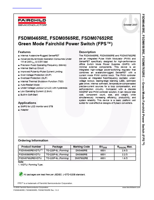
SMPS for LCD monitor and STB Adaptor
Description
The FSDM0465RE, FSDM0565RE and FSDM07652RE are an integrated Pulse Width Modulator (PWM) and SenseFET specifically designed for high-performance offline Switch Mode Power Supplies (SMPS) with minimal external components. This device is an integrated high-voltage power-switching regulator that combines an avalanche-rugged SenseFET with a current mode PWM control block. The PWM controller includes an integrated fixed-frequency oscillator, undervoltage lockout, leading-edge blanking (LEB), optimized gate driver, internal soft-start, temperature-compensated precise-current sources for a loop compensation, and self-protection circuitry. Compared with a discrete MOSFET and PWM controller solution, it can reduce total cost; component count, size, and weight; while simultaneously increasing efficiency, productivity, and system reliability. This device is a basic platform well suited for cost-effective designs of flyback converters.
赛普拉斯推出单芯片True Touch

的一部 分 ,可提供业 界首 批多 种通信 接 口支持 的可 编程 单相位 计量 器件 。 系列微控 制器 支持 电表 、 该 家 庭 自动化 、辅助计 量 以及节 能系统 等计量 应用 的系 统 分 区 ,可实 现 高 度灵 活 的独 立 高 质量 测 量 。
成 电路 C S MS 台 ,该 平 台能够 在单 一芯 片 MO ME 平
上整合 麦克 风的机 械功 能以及其 他包 含模拟 和数 字 电子器 件的传 感器 。 A U3 K 2 0单 片集成 电路麦 克风裸 片 ( 包含 麦克 风膜片、 放大 器 及西 格 玛 一德 尔塔 转 换器 ) 的尺 寸 仅 为 08 m .4 . m X 8 mm,被认 为 是世 界 上 最小 的全 4 0
立2 4位 一 转换 器可帮助 该系列 微控 制器在 △
2 0: 4 01的宽 泛 动态 下 实 现不 足 01 .%的 能 源精 度 误
蒡。
意法 半 导体 推 出 lt r _ 推 出用 于 高速 应 用 的 eS l n
A C驱 动 器 IL 5 1 D 520 S
意法 半导体 扩 大运动 传感器 产 品阵容 ,推 出市
杂 散 动态 范 围 ( F R) 信 噪 比 ( N 性 能 的 超 SD 和 S R)
低失 真 、 低功 耗差分 I / 大器- IL 5 1 。这一 空 O放 - S 52 0
前ห้องสมุดไป่ตู้的高性 能 和低功耗 组合使 客户 能够 实现非 常高效
机、 平板电脑 、 游戏控制以及其它消费电子产品实现
MS 4 0 F P 3 A E系列建 立在 1 6位 R S IC架 构基础 之上 ,
泰克公司推出用于MIPI AIIiance M-PHYSM测试解决方案
能优势 。( 自德州仪器 ) 来
意法半导体 (T 向歌华有线 S) 提供集成机顶盒芯 片
意法半导体 日前宣布北京歌华有线 电视网络公 司的机顶盒已经大规模采用意法半导体集成高清有
线 调 制解 调 器 ( alMoe ) 片 一 T7 4 , 产 C be dm 芯 S i1 1该
通 过将设计规则 紧密结合 到 Cdne aec 实现技
术 , 计 团 队可 以在 编辑 时根据 签 收 D C验证 进行 设 R
检验 , 在其流程 中更早地发现并修正错误 , 同时通过 独立签收解决方案 ,帮助其在漫长的周期 中节省时 间, 实现更快流片。C dne X F B继续紧密合 aec 与 — A 作, 为其混合信号客户提供经检验的签收验证方案。
泰克公 司近 日 宣布 ,推 出用于新 出台 M P Y —H
v. 范 的 MII lac _ H 1 0规 P lne P Y测试 解 决方案 。 A i M. 在
S i1 1 T74 支持 M E 4H24 C 最新高清广播 P G /. / 6V 1
标准 , 集成 D C I E mD c I C b oe 使用 O Ss u O sS al M dm, / e 户可以实现永久在线连接 , 并支持基于 I 协议 的交 P 互电视服务和网络 电话 。S i1 1 T74 具有以太 网接 口 同时支持 D C I3 O SS. 0的信道绑定功能 , 可支持宽带
L 业要 一 界闻
H MI S。 瑞萨 电子认 为 ,这项新技术会成为未来几年 下 载 、 D 以及 U B
惹
【j !j i J
“ 物联网” 产业发展的基础 , 以及实现更高效 的、 有
助 于构 建 生 态 友好 的绿 色 “ 能 城 市 ”的 “ 智 器件 控
MSI中英文对照
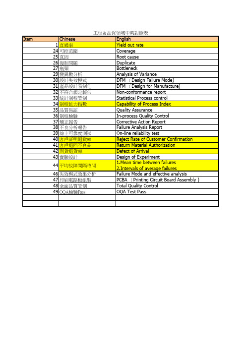
工程&品保領域中英對照表 Chinese English 直通率 Yield out rate 可控范圍 Coverage 真因 Root cause 復制問題 Duplicate 瓶頸 Bottleneck 變異數分析 Analysis of Variance 設計失效模式 DFM (Design Failure Mode) 產品設計易制化 DFM (Design for Manufacture) 不符合規定報告 Non-conformance report 統計制程管制 Statistical Process control 制程能力指數 Capability of Process Index 品質保証 Quality Assurance 制程檢驗 In-process Quality Control 矯正報告 Corrective Action Report 不良分析報告 Failure Analysis Report 線上可靠度測試 On-line reliability test 客戶証明退貨率 Reject Rate of Customer Confirmation 客戶退回不良品 Return Material Authorization 到貨退貨率 Defect of Arrival 實驗設計 Design of Experiment 1.Mean time between failures 平均故障間隔時間 2.Intervals of average failures 失效模式效果分析 Failure Mode and effective analysis 印刷電路板組裝 PCBA (Printing Circuit Board Assembly ) 全面品質管制 Total Quality Control OQA檢驗Pass OQA Test Pass
AS1542中文资料
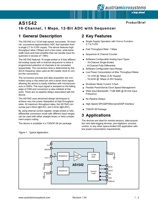
AS154216-Channel, 1 Msps, 12-Bit ADC with SequencerP r o d uc t B r i e f1 General DescriptionThe AS1542 is a 12-bit high-speed, low-power, 16-chan-nel, successive-approximation ADC that operates from a single 2.7 to 5.25V supply. The device features high throughput rates (1Msps) and a low-noise, wide-band-width track-and-hold amplifier that can handle input fre-quencies in excess of 1 MHz.The AS1542 features 16 single-ended or 8 fully differen-tial analog inputs with a channel sequencer to allow a programmed selection of channels to be converted sequentially. The conversion time is determined by the SCLK frequency (also used as the master clock to con-trol the conversion).The conversion process and data acquisition are con-trolled using a chip select pin and a serial clock signal, allowing the device to easily interface with microproces-sors or DSPs. The input signal is sampled on the falling edge of CSN and conversion is also initiated at this point. There are no pipeline delays associated with the device.The AS1542 uses advanced design techniques to achieve very low power dissipation at high throughput rates. At maximum throughput rates, the AS1542 con-sumes just 2.8mA (@3.6V), and 3.5mA (@5.25V). By using internal control register, single-ended or fully-differential conversion mode with different input ranges can be used with either straight binary or twos comple-ment output coding.The device is available in a TSSOP-28 pin package.Figure 1. Typical Application2 Key Features! Single Supply Operation with V DRIVE Function:2.7 to 5.25V! Fast Throughput Rate: 1 Msps ! Sequencer & Channel Counter! Software-Configurable Analog Input Types:-16-Channel Single-Ended -8-Channel Fully-Differential! Software-Configurable Input Range! Low Power Consumption at Max Throughput Rates:-10.1mW @ 1Msps (3.6V Supply)-18.4mW @ 1Msps (5.25V Supply)! Shutdown Mode Current: 0.5µA! Flexible Power/Serial Clock Speed Management ! Wide Input Bandwidth: 71dB SNR @ 50 kHz InputFrequency! No Pipeline Delays! High Speed SPI/QSPI/Microwire/DSP Interface ! TSSOP-28 Package3 ApplicationsThe devices are ideal for remote sensors, data-acquisi-tion and data-logging devices, pen-digitizers, process control, or any other space-limited A/D application with low power-consumption requirements.SCLK AS1542REFINCSN V IN0:15DOUT AGNDMultiplexer16Track/HoldV DD SequencerControl Logic12-Bit ADCDIN VDRIVEGNDDGNDAS1542Product BriefCopyrightsCopyright © 1997-2007, austriamicrosystems AG, Schloss Premstaetten, 8141 Unterpremstaetten, Austria-Europe. Trademarks Registered ®. All rights reserved. The material herein may not be reproduced, adapted, merged, trans-lated, stored, or used without the prior written consent of the copyright owner.All products and companies mentioned are trademarks or registered trademarks of their respective companies. DisclaimerDevices sold by austriamicrosystems AG are covered by the warranty and patent indemnification provisions appearing in its Term of Sale. austriamicrosystems AG makes no warranty, express, statutory, implied, or by description regarding the information set forth herein or regarding the freedom of the described devices from patent infringement. austriami-crosystems AG reserves the right to change specifications and prices at any time and without notice. Therefore, prior to designing this product into a system, it is necessary to check with austriamicrosystems AG for current information. This product is intended for use in normal commercial applications. Applications requiring extended temperature range, unusual environmental requirements, or high reliability applications, such as military, medical life-support or life-sustaining equipment are specifically not recommended without additional processing by austriamicrosystems AG for each application. For shipments of less than 100 parts the manufacturing flow might show deviations from the standard production flow, such as test flow or test location.The information furnished here by austriamicrosystems AG is believed to be correct and accurate. However, austriamicrosystems AG shall not be liable to recipient or any third party for any damages, including but not limited to personal injury, property damage, loss of profits, loss of use, interruption of business or indirect, special, incidental or consequential damages, of any kind, in connection with or arising out of the furnishing, performance or use of the tech-nical data herein. No obligation or liability to recipient or any third party shall arise or flow out of austriamicrosystems AG rendering of technical or other services.Contact InformationHeadquartersaustriamicrosystems AGA-8141 Schloss Premstaetten, AustriaTel: +43 (0) 3136 500 0Fax: +43 (0) 3136 525 01For Sales Offices, Distributors and Representatives, please visit:/contact。
AS1357 LDO 数据手册说明书

AS1357Programmable Triple LDOD a ta S h e et1 General DescriptionThe AS1357 is a high-performance triple CMOS low-dropout voltage regulator in a single QFN package. The efficient set of programmable power supplies is opti-mized to deliver the best compromise between quies-cent current and regulator performance for mobilephones, PDAs, MP3 players, and other battery powered devices.The one-time-programmable (OTP) function provides greater design flexibility by allowing for independent pro-gramming of the output voltage for each regulator on-site. The OTP function allows for fast prototyping reduc-ing development times and costs significant. Factory trimmed versions for full-production are also available.Stability is guaranteed with ceramic output capacitors of only 1µF (±20% – X5R) up to 4.7µF (±20% – X5R). The low equivalent series resistance (ESR) of these capaci-tors ensures low output impedance at high frequencies. Regulation performance is excellent even under low dropout conditions, when the power transistor has to operate in linear mode.The low-noise performance allows direct connection of noise sensitive circuits without additional filtering net-works.The AS1357 is available in a 12-pin QFN 4x4 or 16-pin QFN 3x3 package.Figure 1. Pinout Assignments (Top View)2 Key Features! 3 Independent Voltage Regulators with Shutdown ! Output Current: 200mA each LDO ! One Time Programmable Output Voltage(User- or Factory-Trimmed)! Programmable Output Voltage Range: 1.8 to 3.3V in0.1V Steps! Accuracy: ±1.5%! PSRR: 70dB at 1kHz, 40dB at 100kHz ! Line Regulation: ±2mV ! Load Regulation: ±0.6mV ! Supply Range: 3 to 5.5V! 0.2V Dropout Voltage @ I = 200mA ! Shutdown Current: ≤1µA! Supply Current Without Load: 175µA (typ) ! Softstart for Low Inrush Current! Stable with low ESR Ceramic Capacitors from 1 to4.7µF! Low Noise: 40µV rms @10Hz to 100kHz Bandwidth ! Thermal Protection ! Over-Current Protection! Temperature Range: -40 to +85°C ! Package Types: 12-pin QFN 4x4 and16-pin QFN 3x33 ApplicationsThe AS1357 is ideal for cordless and mobile phones, MP3 players, CD and DVD players, PDAs, handheld computers, digital cameras, and any other hand-held battery-powered device.GNDV OUT2V OUT1EN3N/C REF 13612V DD1051415EN11V DD2V DD4AS135716-pin QFN3x3V DD3V OUT37N/C8V DD9GND11EN216AS135712-pin QFN4x4GNDV OUT3V OUT2V OUT1EN3N/C REF 1069(Exposed Pad)V DD8N/C7541112EN21EN12V DD 3GND13Data Sheet - Pi n o u t4 PinoutPin AssignmentsFigure 2. Pin Assignments (Top View – Not To Scale)Pin DescriptionsTable 1. Pin Descriptions12-pin QFN 4x4 Pin Number 16-pin QFN 3x3 Pin NumberPin Name Description21EN1V OUT1 Digital Input Enable 116EN2V OUT2 Digital Input Enable 1215EN3 V OUT3 Digital Input Enable911, 12GND Negative Supply Voltage .Note:All GND pins must be connected together externally.13 -GND Negative Supply Voltage . This pin is the exposed pad. Note:All GND pins must be connected together externally.1013REF Analog Reference Voltage .Note:Connect to 100nF capacitor during normal operation.3, 82, 3, 4, 9, 10V DD Positive Supply Voltage .Note:All V DD pins must be connected together externally.45V OUT1Regulated Analog Output Voltage 156V OUT2Regulated Analog Output Voltage 267V OUT3Regulated Analog Output Voltage 37,118, 14N/CNot connected.AS135712-pin QFN4x4GNDV OUT3V OUT2V OUT1EN3N/C REF 1069(Exposed Pad)V DD8N/C7541112EN21EN12V DD 3GND13GNDV OUT2V OUT1EN3N/C REF 13612V DD1051415EN11V DD2V DD4AS135716-pin QFN3x3V DD3V OUT37N/C8V DD9GND11EN216Data Sheet- Ab s o l u te M a x i m u m R a t in g s5 Absolute Maximum RatingsStresses beyond those listed in Table 3 may cause permanent damage to the device. These are stress ratings only, and functional operation of the device at these or any other conditions beyond those indicated in the operational sec-tions of the specifications is not implied. Exposure to absolute maximum rating conditions for extended periods may affect device reliability.Table 2. Absolute Maximum RatingsParameter Min Max Units CommentsV DD to GND-0.37VAny other pin to GND-0.3V DD + 0.3VContinuous Power DissipationQFN12 4x4mm11002800mW Min value measured at T AMB = 85°C; max value measured at T AMB = 25°C.Package-Body PeakTemperature 260 °C The reflow peak soldering temperature (body temperature) specified is in accordance with IPC/JEDEC J-STD-020C “Moisture/Reflow Sensitivity Classification for non-hermetic Solid State Surface Mount Devices”.Operating Temperature-4085°CStorage Temperature-65150°CElectrostatic DischargeProtection (ESD) Level 1kV HBM – Norm: MIL 883 E method 3015.Data Sheet - El e c t ri c al C ha r a c te r i s ti c s6 Electrical CharacteristicsV DD = 4V; T AMB = -40 to +85°C (Typ values are for T AMB = 25°C); C LOAD = 1µF (Ceramic); unless otherwise specified .Notes:1. Guaranteed by design and verified by lab evaluation.2. Startup is performed if any EN pin goes high.Table 3. Electrical Characteristics Symbol Parameter ConditionsMin TypMax Unit V DD Supply Voltage Range 3 5.5V V OUT Output Voltage Range1.83.3V R ON On Resistance 1ΩPSRR 1Power Supply Rejection Ratio f = 1kHz, C REF = 100nF 70dB f = 100kHz, C REF = 100nF40I OFF Shut Down Current ENx = Low 1µA I VDD Supply Current Without Load175275µA t set 1Output Voltage Settling Time I LOAD Switched from 0 to 100mA 50µs t start 1Start-up Time 2C REF = 100nF Pre-charged300µs C REF = 0nF Uncharged 300µs C REF = 100nF Uncharged15ms V OUTOutput Voltage ToleranceI LOAD = 0mA, T AMB = 25°C-1.5 1.5%I LOAD = 0 to 200mA-22%V LINEREG Line Regulation, StaticV DD = 5.5V -11%V DD = 3 to 4.5V -22mV 1V LOADREGLoad Regulation, Static I LOAD = 0 to 50 mA0.3 2.5mV 1I LOAD = 0 to 200 mA (referenced to 100mA)0.65mV 1V IH Enable Input Voltage High 0.6 x V DDV V IL Enable Input Voltage Low0.8V I LOAD Output Current 0200mA I LIMIT Output Current Limitation 400mA V NoiseOutput Noise Voltage 10 to 100kHz, C REF = 100nF40µV RMS Thermal Protection145°C7 Typical ApplicationFigure 3. Typical AS1357_uxy ApplicationOne-Time Programming Procedure Output VoltagesThe three LDOs can be programmed and burned to any output voltage between 1.8 and 3.3V in steps of 0.1V. Cus-tomers can burn the desired output voltages onsite using the austriamicrosystems programming board.Furthermore, the AS1357 is available in pre-programmed versions with fixed output voltages (see Ordering Information on page 9.)1µF ±20% (X5R)2.2µF +100/-50% (Z5U)V PERIV CORECMOS Sensor2.8V2.5VV PERIMicroprocessor2.8V100nF (Improved Noise Performance)MicroprocessorAS1357_A7AV OUT11µF ±20% (X5R)2.2µF +100/-50% (Z5U)V OUT21µF ±20% (X5R)2.2µF +100/-50% (Z5U)V OUT3V DDEN1EN2EN3GND GNDREF3VFigure 4. AS1357 Block DiagramThermal Protection Overcurrent Protection SoftstartControlThermal Protection Overcurrent Protection SoftstartControlReference VoltageThermal Protection Overcurrent Protection SoftstartControlV DDV DDV REFV REFV REFEN1EN2EN3GNDREFV OUT1V OUT2V OUT3AS1357Data Sheet- Pa c k ag e D r a w i n gs a n d M a rk in g s8 Package Drawings and MarkingsThe AS1357 is available in a 12-pin QFN 4x4 package and a 16-pin QFN 3x3 package. Figure 5. 12-pin QFN 4x4 and 16-pin QFN 3x3 PackagesNotes:1. Dimensioning and tolerancing conform to ASME Y14.5M-1994.2. All dimensions are in millimeters; angles in degrees.3. N is the total number of terminals.4. The terminal #1 identifier and terminal numbering convention shall conform to JEDEC 95 SPP-012. Details of termi-nal #1 identifier are optional but must be located within the zone indicated. The terminal #1 identifier may be either a mold or marked feature.5. Dimension b applies to metallized terminal and is measured between 0.15 and 0.30mm from terminal tip. If one end of the terminal has the optional radius, the b dimension should not be measured in that radius area.6. Dimensions ND and NE refer to the number of terminals on each D and E side, respectively.7. Depopulation is possible in a symmetrical fashion.8. Figure 5 is shown for illustration only and does not represent any specific variation.9. All variations may be constructed per Figure 5, however variations may alternately be constructed between square or rectangle shape per dimensions D and E.10. Refer to the Dimensions Table for a complete set of dimensions.11. Bilateral coplanarity zone applies to the exposed heat sink slug as well as the terminals.12. Depending on the method of lead termination at the edge of the package, pullback (L1) may be present. L minusL1 to be ≥ 0.33mm.13. For variations with more than one lead count for a given body size and terminal pitch, each lead count for that vari-ation is denoted by a dash number (e.g., -1 or -2).12-pin QFN 4x4 Dimensions SymbolMinNom MaxNotes aaa0.151, 2bbb 0.101, 2ccc 0.101, 2ddd 0.051, 2b 0.250.300.351, 2e 0.80A 0.800.90 1.001, 2A10.000.020.051, 2A30.20 REF1, 2L10.030.151, 2D BSC 4.001, 2, 10E BSC 4.001, 2, 10D2 2.00 2.15 2.251, 2, 10E2 2.00 2.15 2.251, 2, 10L 0.450.550.651, 2, 10N 121, 2, 10ND 31, 2, 10NE31, 2, 1016-pin QFN 3x3 Dimensions Symbol MinNom MaxNotes aaa0.151, 2bbb 0.101, 2ccc 0.101, 2ddd 0.051, 2b 0.180.250.301, 2e 0.50A 0.800.90 1.001, 2A10.000.020.051, 2A30.20REF1, 2L10.030.151, 2D BSC 3.001, 2, 10E BSC 3.001, 2, 10D2 1.30 1.45 1.551, 2, 10E2 1.30 1.45 1.551, 2, 10L 0.300.400.501, 2, 10N 161, 2, 10ND 41, 2, 10NE41, 2, 109 Ordering InformationThe AS1357 is available with preset LDO output voltages or customer-specific versions (with a minimum order quantity of 30,000). Each customer-specific device is factory trimmed to the desired output voltage (see Table 9).Table 4. Ordering InformationPart LDO ValuesDelivery Form Package AS1357-T User-programmable LDO values 11.The values are programmed via the AS1352/57 programming board.Tape and Reel12-pin QFN 4x4AS1357User-programmable LDO values 1Tray 12-pin QFN 4x4AS1357V-T 22.Available upon request. Contact austriamicrosystems, AG for more er-programmable LDO values 1Tape and Reel16-pin QFN 3x3AS1357V 2User-programmable LDO values 1Tray 16-pin QFN 3x3AS1357_A7A-T V OUT1 = 2.8V, V OUT2 = 2.5V, V OUT3 = 2.8VTape and Reel12-pin QFN 4x4AS1357_uxy-T 3, 43.Customer-specific values are as follows:u = Customer-specific V OUT1 value suffix.x = Customer-specific V OUT2 value suffix.y = Customer-specific V OUT3 value suffix.4.“-T” suffix for tape and reel, no suffix for tray delivery form.Customer-specific LDO values --- 12-pin QFN 4x4AS1357V_uxy-T 2, 3, 4Customer-specific LDO values---16-pin QFN 3x3Table 5. Output Voltages Suffix GuidePartSuffix Output VoltageAS1357_uxyF 3.3 V E 3.2 V D 3.1 V C 3.0 V B 2.9 V A 2.8 V 92.7 V 8 2.6 V 7 2.5 V 6 2.4 V 5 2.3 V 4 2.2 V 3 2.1 V 2 2.0 V 1 1.9 V 01.8 VData Sheet- Or d e ri n g I nf or m a ti o nCopyrightsCopyright © 1997-2007, austriamicrosystems AG, Schloss Premstaetten, 8141 Unterpremstaetten, Austria-Europe. Trademarks Registered ®. All rights reserved. The material herein may not be reproduced, adapted, merged, trans-lated, stored, or used without the prior written consent of the copyright owner.All products and companies mentioned are trademarks or registered trademarks of their respective companies. DisclaimerDevices sold by austriamicrosystems AG are covered by the warranty and patent indemnification provisions appearing in its Term of Sale. austriamicrosystems AG makes no warranty, express, statutory, implied, or by description regarding the information set forth herein or regarding the freedom of the described devices from patent infringement. austriami-crosystems AG reserves the right to change specifications and prices at any time and without notice. Therefore, prior to designing this product into a system, it is necessary to check with austriamicrosystems AG for current information. This product is intended for use in normal commercial applications. Applications requiring extended temperature range, unusual environmental requirements, or high reliability applications, such as military, medical life-support or life-sustaining equipment are specifically not recommended without additional processing by austriamicrosystems AG for each application. For shipments of less than 100 parts the manufacturing flow might show deviations from the standard production flow, such as test flow or test location.The information furnished here by austriamicrosystems AG is believed to be correct and accurate. However, austriamicrosystems AG shall not be liable to recipient or any third party for any damages, including but not limited to personal injury, property damage, loss of profits, loss of use, interruption of business or indirect, special, incidental or consequential damages, of any kind, in connection with or arising out of the furnishing, performance or use of the tech-nical data herein. No obligation or liability to recipient or any third party shall arise or flow out of austriamicrosystems AG rendering of technical or other services.Contact InformationHeadquartersaustriamicrosystems AGA-8141 Schloss Premstaetten, AustriaTel: +43 (0) 3136 500 0Fax: +43 (0) 3136 525 01For Sales Offices, Distributors and Representatives, please visit:/contact。
ADM1040资料
=Power Supply Monitor ASICADM1040FEATURESMonitors Multiple Volta ge Ra ils (240VA Lim-ited)Monitors Bulk DC, Op-Amp Supply, 5V Supply Monitors Volta ge Ra ils 1,2 a nd 3 Currents Up to 3 Fa n Speed Mea surement Cha nnels Up to 6 General-Purpose Logic InputsExterna l Tempera ture Mea surement with Remote Diode (Two Channels)On-Chip Tempera ture SensorLimit Compa rison of a ll Monitored Va luesFUNCTIONAL BLOCK DIAGRAMREV. PrG 01/'01Information furnished by Analog Devices is believed to be accurate and reliable. However, no responsibility is assumed by Analog Devices for its use, nor for any infringements of patents or other rights of third parties which may result from its use. No license is granted by implication or otherwise under any patent or patent rights of Analog Devices.One Technology Way, P .O. Box 9106, Norwood, MA 02062-9106, U.S.A.Tel: 617/329-4700World Wide Web Site: Fax: 617/326-8703© Analog Devices, Inc., 2001Preliminary T echnical D ataSMBus is a trademarkAna log Fa n Speed Control Output SMBus TM Compa tible Seria l Interfa ce SMBus ALERT Ca pa bility512 Bytes On-Chip, Write-Protected E 2PROM Shutdown Output for Overtemperature and 240VA FaultsAPPLICATIONSNetwork Servers and Personal Computers Microprocessor-Ba sed Office Equipment Test Equipment and Measuring InstrumentsPRELIMINARY TECHNICAL DATAGNDSCL SDA A0/NTEST_OUT V DD /5VSBGPI3/I2_-/AIN2D1-/GPI2D1+/GPI3D2-/GPI4/FAN2D2+/GPI5/FAN3I1_-/AIN1AIN3AIN4AIN5GPI0FAN1/GPI1ALERTA1SHDNDAC/NTEST_IN元器件交易网。
831 Aerosol Mass Monitor 小型可靠低成本气体质量监测仪说明书
831 Aerosol Mass Monitor Small - Reliable - AffordableFour Mass Ranges (PM1, PM2.5, PM4, PM10)A mass monitor that simultaneously provides data of four important mass ranges in one minute. Battery Powered24 hours of typical intermittent operation and up to 8 hours of continuous use. Recharge time is only2.5 hours. The included AC charger / adapter operates the counter even when the batter pack is discharged. Simple OperationOnly two front-panel buttons accompany the multifunction rotary scroll wheel to provide simple and efficient operation. Just press and rotate to scroll thru the menu driven platform.Sample HistoryView sample history easily on the display or export data via the USB port using the included software. Unit stores up to 2500 sample events. USB interface provides quick data download and field firmware upgrades.ApplicationsIndustrial/occupational hygienePoint source location monitoring Indoor/Outdoor Air QualityProcess Control HVAC Applications Filter Testing Mining & Ore Processing Remote Sampling Handheld OperationSurvey the environment with this extremelyportable, size selective mass monitor. This small lightweight instrument is only 28 ounces and is the perfect survey tool for a wide range of applications. Whatever your particular needs, The right choice is only natural.Met One Instruments, Inc. Figure 1 – Model 831 pictured with optional protective bootSpecifications 831 Operating Principle Particle count to mass conversion FeaturesSample Duration 1 minute Data storage2,500 records Display2-line by 16-character LCD Controls2 button keypad with rotary dial Performance PM RangesPM1, PM2.5, PM4 and PM10 Concentration Range 0 – 1,000 µg/m 3 Resolution0.1µg/m 3 (display / serial output) Sensitivity0.5µm Accuracy± 10% to calibration aerosol Flow rate0.1 CFM (2.83 lpm) ElectricalLight SourceLaser Diode, 780 nm, 40 mW typical AC Adapter/Charger AC to DC module, 100 – 240 VAC to 8.4 VDC Battery TypeLi-ion rechargeable Battery Battery Operating Time 8 hours continuous operation 24 hour intermittent operation Battery Recharge Time 2.5 hours typical Communication USB Mini B Type PhysicalSizeHeight: 6.25” (15.9 cm) Width: 3.63” (9.22 cm) Thickness: 2.00” (5.08 cm) Weight1.74 lbs – 28 ounces – (0.79 kg) EnvironmentalOperating Temperature 0º C to +50º C Storage Temperature -20º C to +60º C Accessories SuppliedBattery charger / adapterUSB CableOperation manualComet software OptionalCarrying Case (P/N 8517)Protective Boot (P/N 80450)Zero Filter Kit (P/N 80846)Flow Meter Kit (P/N 80530) 1600 Washington Blvd., Grants Pass, OR 97526 Tel: 541.471.7111 | Fax: 541.471.7116 E-mail: ********************|Met One Instruments, Inc. 5/8/2012。
S32K 培训资料 单片机介绍
KFA family, rev A
Carl Culshaw, Systems Engineering, Automotive MCU
Oct 24.2014
TM
Confidential and Proprietary
Complex Safety Function
(e.g. EPS)
Simple Safety Function
(e.g. Airbag)
ASIL D target ASIL C target ASIL B target ASIL A target
EPS, ESP, Engine Vision based Management ADAS… MCU HEV… HW
(10.9 Safety Element out of Context)
SafeAssure Standard HW Airbag, Body, DIS…
(8.13 Qualification of Hardware Components)
Enabled for ISO 26262
Where we enable the customer to do the Qualification, testing and analysis to prove that our component is suitable for the purpose of his safety concept.
8
Functional Safety
Single Point Fault Metric
• •
Diversity of safety levels
AS-Interface数据解耦单元说明书
Data sheet3RK7271-1AA30-0AA0SIMATIC S7-1200, DCM 1271, DATA DECOUPLINGMODULE, FOR AS-I MASTER CM 1243-2 IN: DC 24 V /30 V OUT: 1 X AS-I, 4 A INTEGR. OVERLOADPROTECTION, INTEGR. EARTH FAULT DETECTION,SIGNALING CONTACT
General technical data:product brand nameAS-InterfaceProduct designationAS-Interface data decoupling unitDesign of the productCommunication module 30 mm for SIMATIC S7-1200Protection class IPIP20Installation altitude at height above sea levelmaximumm2 000
Ambient temperature● during operation°C0 ... 55● during storage°C-40 ... +70Relative humidity at 25 °C during operation maximum%95Equipment marking acc. to DIN 40719 extendedaccording to IEC 204-2 acc. to IEC 750A
Equipment marking acc. to DIN EN 61346-2AActive power suppliedW120Product function● Auto-resetYes● External resetNo● Manual RESETNo● Ground fault detectionYes● Test function of signaling contactsNo● suitable for grounded AS-i networksYes● adapted for non-grounded AS-i networksYes● suitable for AS-i Power24VYes● sequential connected time-delayNo
- 1、下载文档前请自行甄别文档内容的完整性,平台不提供额外的编辑、内容补充、找答案等附加服务。
- 2、"仅部分预览"的文档,不可在线预览部分如存在完整性等问题,可反馈申请退款(可完整预览的文档不适用该条件!)。
- 3、如文档侵犯您的权益,请联系客服反馈,我们会尽快为您处理(人工客服工作时间:9:00-18:30)。
2 4l
蠡 塞 21 2 第 期 I o 年 月 1 2
导体设备供应商 ,在 中国拥有完善 的销售与服务体系及
扎实的客 户基础 。由美亚作为我们在 中国的战略合作伙 伴,也是我们进军中国市场 的重要策略之一。”
.
您将可 以更轻松地应用古老的流程优化准则,即 “ 无 您 法改进您不能衡量 的方面 ”。这一软件能够实时收集 有 关各种机器和生产线 的全部性能参数 。由于用户也可 以 在软件中为其重要 的关键性能指标 (P )输入 目标值, II (
随着全新SP AE P rom n eM n rn 的推 出, IL C e fr ac oi oig t
泰 时 自动 系统 携 手 美 亚进 军 中国市 场
全球领先 的半导体及 电子设备之设计及制造供 货商
泰时 自动系统有 限公司 ( ISA T MT O ) 日前正式与 D A U O AIN
优化 效率和加强亮度, 更提供极高可靠性能并且 降低光通
量单 位 的成本 。 ”A PA LH 能源 技术 副总裁 Rv h ta a i Ba k l
m ne M nt rn 的实 时比较功能 ,我们 能够支 持技术 ac o io ig 人 员和操作人员更有效地开展性能改进工作 。过去的经 验表 明,如果您 能够及时按班次提供偏差相关信息 ,操 作 人员将 能够更早采取相关应对措施 ,进而在许多情况 中能够取得更大 的成功 。由于 目标值可在各个生产环节
美亚科技确立战略合作伙伴关系 ,美亚科技将作为DA IS 在 中国地 区的主要代理 ,负责DA 旗 下产品在中国市场 IS
的经销事务 。
DA E 梁伟生表示 : “ IS CO 目前,中国在 全球半导体
产 品生产 中的份额在 日益增加 ,但 中国的半导体产 品生
产 的规模 并没有赶上其消费速度 ,产业缺 口仍十分 巨大, 我们 非常看好 中国的半 导体产业前景 。美亚是成熟 的半
根 据进展情况进 行调整 ,SPA E Pr om n eM n tr ILC ef ra c o io
说。 “ 我们举世 闻名的专业焊接材料知识 , 让我们能深入 了解LD装配过程会遇到的各种具挑觇 }的难题。” E 生 A PA Lm t A 焊膏产品系列和新的M XE 金 LH u e SC A RL 合
成 型焊锡、SC ls AX P u ;低银合金焊条 、Ag mx ro a烧结 银
产 品以及A rx 电胶 。 to 导
A M全 新 推 出 SP A efr n e S IL CE P r ma c o
Mo i r g nt i o n
A M A sm l y tm 宣 布 推 出另 一 项 软 件 创 新 S s eby Ss es SPA E P r omn e M n trn 。此软 件 能够 实 时确 ILC efr ac oio ig 定生产线状态和重要的关键性能指标 ( I 。这些指标 以 K ) P 绝对值 的形式,在 易于观看 的实时K I 目标 比较 图中显 P与 示 ,同时此类图表 中还包含有可轻松定制 的参考值 。此 软件 不仅 可 以为 技术 人员 和流程 工程 师提 供详细 的信 息 ,同时还能够通过大尺寸显示屏让生 产人员掌握最新 情况 ,包括订单进展、 目标实现 情况和 各个环 节可能的 改进 ,如吞吐时间、物料设置时间、贴装速率 、元件抛 料率和单板生产周期时 间等。
分图表 也可 以在工厂 中的大尺寸显示器上显示 ,为员工 提供有关其活动的班 次相关 数据 ,以及改进建议 。在此 基础之上 ,员工能够 更轻松地监控 有关订 单进展 、吞吐
未来规划让我们看到 了更多的商机与发展空间 。七 大战
略领域都和半导体行业有直接和间接的关系。我们期望 通过与DA 的战略合作 ,加 强并深化 我们在 中国半导体 IS 产业的发展。” 0
领域并提供客户一个最具性价 比的设备。
实时K I 目标 比较 图中,显示有关单个工厂 、S I P与 M 生产 线或班次的信息。 更 多生产线信息和行动
美亚科技半导体部 的何建锡表示 : “ IS DA 全线 设备 将对我们现有半导体业务体系的加强与延伸 。十二五的
进 展和性 能数据在现实和 目标 值 比较 图中的图形化 显示 ,对 于技 术人 员和工程师有着重要作用 。同时 ,部
SP AE P ro mn e M nt rn 还 能够在 易于观 看 的 IL C e fra c o io ig
DA 公司 的主打产 品第三ቤተ መጻሕፍቲ ባይዱ光学检查 设备I一 3 IS s3 /
I一 视像检验设备将帮助封测厂更快 的查纠生产 问题 、 s5 高度集成的软件也帮助工厂数据的一体化整合 。DA 公 IS 司生产的超声波 自动焊 线机 ,固晶机 以及高精度 点胶机 系统是具有竞争力、先进 性的机 型适用于专 门的半 导体
在本次盛会上推 出。这些新产品能提供 极优异 的热循环
性能 ,优化抗振动能力并大大 降低LD E受到的热辐射 。此
外,还将展 出AP A 有芯焊 丝、E at lo ;MXE 预 LH xc a ly AR L
ig n 将能够支持制造商在 电子生产过程中不断改进流程 。 SPA E P rom n e M n trn 支 持在 生 产过 程 ILC ef ra c o io ig 中更有效分析现实情况与 目标的偏差, 以及实际性能 。
及透 彻 了解客户在L D E 生产过程 中的需求, 从而在每个关
键制造步骤 中创造价值 的成果 。我们 的产 品不仅关注于
时间或丢弃率偏差,采取纠正措施 ,并查看成功情况。 S PAE IL C 中国软件部门负责人李飞涛表示 : “ 明度 透
是任意流程优化工作的先决条件 。通过SPA E P ro— ILC e fr