Optically induced effects in thin films of indandione type organic 在2型有机薄膜光诱导的影响
双钙钛矿Ba2LuNbO6∶Tb3+闪烁体多模式X_射线探测

第 44 卷第 9 期2023年 9 月Vol.44 No.9Sept., 2023发光学报CHINESE JOURNAL OF LUMINESCENCE双钙钛矿Ba2LuNbO6∶Tb3+闪烁体多模式X射线探测岳杨1,郭龙超1,刘昊哲2,卜卫芳1,徐旭辉3,谢俊奎4,仇广宇4,王婷2*,余雪1*(1. 成都大学机械工程学院,四川成都 610106; 2.成都理工大学材料与化学化工学院,四川成都 610059;3. 昆明理工大学材料科学与工程学院,云南省新材料制备与加工重点实验室,云南昆明 650093;4. 交通运输部南海航海保障中心北海航标处,广西北海 536000)摘要:采用高温固相法制备了双钙钛矿结构的Ba2LuNbO6∶x Tb3+(x = 0.01,0.02,0.05,0.10,0.20)闪烁体材料,并系统地研究了其晶体结构、形貌和X射线激发的光学性能。
研究表明,在X射线激发下,Ba2LuNbO6∶Tb3+的发射光谱主要由Tb3+的特征发射组成,其中最强发射峰位于545 nm处。
X射线发射(RL)强度随Tb3+浓度的增加逐渐增大,当x = 0.1时发射强度达到最大值。
此外,X射线辐照5 min后的热释光(TL)曲线显示该样品存在位于T1(377 K)和T2(460 K)的两个陷阱。
其陷阱深度分别为0.754 eV和0.920 eV,这表明该材料具有潜在的X射线信息存储性能。
因此,我们可通过加热或者980 nm激光二极管激发,有效诱导读出存储在深陷阱中的载流子,实现高亮度光激励发光(PSL)和热刺激发光(TSL)。
基于此,由Ba2LuNbO6∶Tb3+与聚二甲基硅氧烷(PDMS)所制备的柔性闪烁体薄膜,在低X射线剂量辐照下表现出优异的X射线成像分辨率(12.5 lp/mm)以及延时成像特性。
以上结果表明,所制备的Ba2LuNbO6∶0.1Tb3+在X射线探测和X射线信息存储方面具有潜在的应用前景。
焙烧温度对TiO2薄膜的光催化氧化性能的影响

焙烧温度对TiO2薄膜的光催化氧化性能的影响
焙烧温度对TiO2薄膜的光催化氧化性能的影响
采用溶胶-凝胶法制备TiO2薄膜(玻片为载体),比较在不同的焙烧温度下制备的TiO2薄膜对有机物的光催化氧化性能,用D/XAX-1200全自动X射线衍射仪检测在不同的焙烧温度下制备的TiO2薄膜的晶型结构,计算其锐钛型和晶红石晶型所占比例,从而确定通过控制焙烧温度来控制各种不同比例的晶型结构,提出温度对TiO2薄膜对有机物的光催化氧化性能的影响机制.
作者:刘仁龙张丙怀张云怀作者单位:刘仁龙(重庆大学,动力工程学院,重庆,400044)
张丙怀(重庆大学,材料科学与工程学院,重庆,400044)
张云怀(重庆大学,化学化工学院,重庆,400044)
刊名:重庆大学学报(自然科学版) ISTIC EI PKU英文刊名:JOURNAL OF CHONGQING UNIVERSITY(NATURAL SCIECNE EDITION) 年,卷(期):2002 25(7) 分类号:O644 关键词:焙烧温度 TiO2薄膜晶型光催化活性。
扫描隧道显微镜
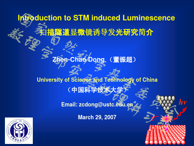
国 家 数 自 理 hv 然 学 科 e 部 学 实 基 验 金 物 委 理 }员 讲 会 习 班 I=I + I
Definition: STM Induced Luminescence (STML) Beyond imaging and manipulation Elastic Tunneling Process:
Theoretical calculations
国 Introduction to the Background Brief 家 数 自 理 然 学 科 部 学 Experimental Techniques 实 基 验 金 物 委 Status of STM Induced Luminescence 员 理 讲 会 习 班
_
hv
原子分辨 STM
+
e–
ET
e–h
单光子计数 Optical Detectors
h+
recombination
HT
空间、能量、时间 高分辨
+
能量转化动力学
纳米元件、生物分子识别?
国分子尺度调控研究的多功能复合技术 家 数 自 理 扫描探针技术 伏安曲线测量 光学技术 然 学 科 部 学 实 基 验 金 物 委 + “Z” (X,Y) (X,Y) 理 (X,Y) + I-V 员 讲 + dI/dV 会 (X,Y) 习 (X,Y) 班 I/dV + d
Interface parameter control for organic electronics (e.g., OLED, η↑) Spectral imaging of single defects or impurities in electronic devices Radiative decay engineering for bio-molecular (DNA) mapping Nanoscale light source for optical spectroscopy and imaging Single-molecule electroluminescence and single-photon sources
SSPC-Paint 20
Editorial Revisions November 1, 2004
SSPC: The Society for Protective Coatings
PAINT SPECIFICATION NO. 20
Zinc-Rich Coating Type I – Inorganic and Type II – Organic
Paint 30
Weld-Through Inorganic Zinc
Primer
SP 1
Solvent Cleaning
SP 5/NACE No. 1 White Metal Blast Cleaning
PS Guide 12.00 Guide to Zinc-Rich Coating
Systems
* PS 12.01
One-Coat Zinc-Rich Painting
System
3.4 ASTM INTERNATIONAL STANDARDS:1
A 572 Standard Specification for High-Strength Low-Alloy Columbium-Vanadium Structural Steel
Level 1 — equal to or greater than 85% Level 2 — equal to or greater than 77% and less
than 85% Level 3 — equal to or greater than 65% and less
than 77%
1.5 This coating is intended for application by spray for use by itself or as a primer in a multi-coat system.
银铜双金属薄膜的激光诱导换膜和光伏性质
d p s e n teT O u srt i I T p o e sn .I o ta t oJ— Vc re fTO2 h ta o e i e oi d o h i 2s b t ew t L F r c sig n c nrc t a h t uv so i oo n d ,sl p —
o t O2s b ta e frv ro s c n r le a e r c s i g p r mee s a d c p e n o a Ti u sr t o a iu o to ld ls rp o e sn a a t r n o p r—sle o o iin r — i rc mp sto a v to .Th i co tu t r is e r mir sr c u e,moph lg n h tv l i r p ris we e h r ce ie b r oo y a d p o o ot c p o e t r c a a t rz d y XRD, S a e EM ,
g r o n c r u tv la e wih i c e sn ft e mo a ai fsl e n t e bi t l c fl . e pe ic i ot g t n r a i g o h lrr to o i ri h meal ms v i i
s bsr t c me s le fe F a d t e ut d p oo a o e e h b t ih rs o ic i u e td n— u ta ebe o mal rat rLI T n he r s l h t n d x i ish g e h r cr u tc r n e e t st n a g r o e ic i o tg iy a d l r e p n cr u t v l e,whih i c e s d wh n t ls r pr c si g po r i u h r i a c s de r a e e he a e o e sn we s f r e m— t
nature
本科生科研训练题目高能量密度柔性赝电容器中的二维磷酸氧钒超薄结构(翻译)院系物理科学与技术学院专业物理学基地班年级2012级学生姓名李赫学号**********二0一三年十二月二十日natureCOMMUNICATIONS2013年2月5号收到稿件2013年8月12日接受稿件2013年9月12日发表稿件DOI: 10.1038/ncomms3431高能量密度柔性赝电容器中的二维磷酸氧钒超薄结构二维材料一直以来在柔性薄膜型超级电容器,以及表现有关灵活性,超薄度甚至透明度的强劲优势上都是一个理想的构建平台。
要探索新的具有高电化学活性的二维赝电容材料,我们需要获得具有高能量密度的柔性薄膜超级电容器。
这里我们介绍一个无机石墨烯类似物,a1钒,一种少于6个电子层的磷酸盐超薄纳米片来作为一个有发展前景的材料去构建柔性全固态超薄赝电容器。
这种材料展示了一个在水溶液中氧化还原电位(~1.0V)接近纯水电化学窗口电压(1.23V)的赝电容柔性平面超级电容器。
通过层层组装构建出的柔性薄膜型超级电容器的氧化还原电位高达1.0V,比容量高达8360.5 μF∙cm-2,能量密度达1.7 mWh ∙cm-2,功率密度达5.2 mW∙cm-2。
现在,便携式消费电子产品的需求在快速增长,如柔性显示器,手机和笔记本电脑,极大推动了在全固态下的柔性能源设备的开发。
作为未来一代的储能装置,柔性薄膜型超级电容器在全固态下提供柔韧性,超薄型和透明度的协同效益。
在不同的类型的超级电容器中,与电双层电容器相比,赝电容器因为自身的高活性表面的电极材料可以快速发生的氧化还原反应而具有明显优势。
与锂离子电池相比,它表现出更高的能量密度,以及更高的功率密度。
因此,承载着为实现高性能的柔性薄膜型超级电容器的全固态伟大的承诺(FUSA)与电容行为。
具有赝电容特性的二维(2D)类石墨烯材料代表着一个有前途的方向可以去实现全固态下的高能量密度柔性超级电容器,和潜在的优良的机械柔性。
NBTIPMOS薄栅氧PMOS器件的HCI效应和NBTI效应
可靠性:PMOS 薄栅氧PMOS 器件的HCI 效应和NBTI 效应《半导体制造》 2006 年 10 月刊作者: Joyce Zhou 、 Jeff Wu、 Jack Chen 、 Wei-Ting Kary Chien, 中芯国际随着 CMOS 晶体管尺寸的不断微缩,人们越来越关注 PMOS HCI(热载流子注入)可靠性问题。
本文对薄栅氧PM OS 晶体管的可靠性进行了准确的表征,并且深入研究了其衰减机制。
此外,我们还对引起PMOS 器件衰减的 N BTI(负偏压温度不稳定性)效应进行了解释说明。
对 PMOS 而言,最坏的衰减条件与 Vg 大小非常相关。
为此,我们提出一种方法以证明 PMOS 衰减是在较大Vg 条件下由HCI 效应导致的漏极缺陷引起的,它与NBTI 效应完全不同。
此外,我们还分别解释了HCI 和 NBTI 效应的机理。
最后,我们研究了 HCI和NBTI 的综合效应。
在 HCI 和NBTI的综合作用下,超薄栅氧 PMOS 器件参数的衰减程度比单独的 HCI 或 NBTI 效应要严重得多。
为了找到薄栅氧 PMOS 器件 HCI效应的最坏条件,实验中我们对 1.2V和1.5V 短沟道 PMOS 器件进行了测试。
我们提出了一种在较高栅电场下区分 HCI 效应和 NBTI 效应的方法。
此外,我们还对这两种效应(即 HCI 和 NBTI)导致的器件参数偏移之间的相关性进行了研究,并且探讨了 HCI-NBTI 综合效应对薄栅氧 PMOS 器件可靠性的严重影响。
下一节我们将介绍 HCI 的最坏条件。
为了检测 HCI 效应引起的漏极损伤问题,我们在下一节中引入了“偏移”参数(Offset)。
然后,我们对非均匀 NBTI 效应进行了描述。
薄栅氧 PMOS 器件 HCI 效应的最坏条件正如JEDEC-60 提到的那样,在施加大小为 Vg 的栅偏压条件下, p沟道器件的参数变化程度最大,此时栅电流也处于最大值(Ig)[1] 。
周利芬翻译
纳米Cu-ZnO, Cu-CdO, CuO的固相合成及温度对其光学性能的影响摘要:控制新颖的形态和发展有效的掺杂的策略是促进两个重要的任务基于纳米ZnO 和CdO。
大小控制通过调制频带能量提供了新的控制的太阳能电池的光响应和光电转换效率的方法。
P型半导体CuO和ZnO是用于光伏电池的一个重要的功能材料。
CuO的吸引力在于作为一种选择性太阳能吸收器由于具有高的太阳能吸收率和低的热辐射率。
这项工作介绍了半导体纳米粒子的合成与表征(ZnO,CuO,Cu-CdO,ZnO,Cu-CdO)通过一步,在聚乙二醇400存在下的固态反应。
1.简介自从1991年教授在染料敏化太阳能电池(DSSCs)上发表了历史论文后,由于其低廉的成本和广泛的科学兴趣,染料敏化太阳能电池已经迅速吸引了大量的来自不同领域的人的注意。
【1-3】最大的DSSCs的太阳能能源电力转换效率已经从%提高到11%,各种最近的努力主要是面向发展更好的无机电极材料和有机敏化剂。
【4】已经有越来越多的研究致力于掺杂半导体,掺杂是一个功能强大的工具定制的光学和电学性能。
Cu掺杂修改通过创建本地化的杂质在ZnO发光跃迁水平。
此外,铜作为其能量在ZnO受体水平位于的下方的导带的底部,使其成为创建P型ZnO的很好的实验对象。
【1】ZnO是一种重要的和通用的在室温下有的直接带隙宽的半导体。
其强大的激子为60meV结合能使它对激光的激子应用具有强大的吸引力。
ZnO也在太阳能电池、气体传感器、光催化、光电探测器、光电二极管、光调制器、化学和生物传感器、压敏电阻、透明薄膜、晶体管等方面具有巨大的潜力。
【1-6】最近,在研究前沿的ZnO纳米材料在基本的科学和潜在的先进技术激发方面取得了巨大的进展。
ZnO(粉的形式)被用来制备第三代太阳能电池即染料敏化太阳能电池(DSSCs)。
【2】由于其较低的制造成本、耐久性、环境相容性和简单的制造过程,对小型电子设备和光电致变色窗低功率器件的应用兴趣已经大幅增长。
光学薄膜技术-02光学特性(3)
E0 E11, E0 E11 E0 E0 E0 E11 E11 E11
H 0
H
0
H
0
H11
H11
H11
于是,可得:k0
E0
k0
( E11
E11 )
H 0 (H11 1 (k0 E11) 1(k0 E11) 1(k0 E11 k0 E11)
(2)在界面1,2的内侧,不同纵坐标、相同横坐标的两点,只要改变波的位相因子,
a)
b)
当膜的光学厚度取 0 4 的偶数倍时,反射率也是极 值,且视它们的折射率而定, 只是情况恰巧相反,如图所 4示。
图4 单层介质膜的反射率随其光学厚度的变化关系,其
中n0=1,n2=1.5,膜的折射率为n1,入射角 0 0。
20
单层介质膜的光学特性
注意:
(1)因为R是 的函数,所以,这里所说的“极值”、“虚
系和基底的参数N1 、 N2、d1等有关);
➢基于等效界面思想,建立 E0与E2 '、H0与H2的' 联系,又有等效介 质的等效光学导纳Y和介质2的光学导纳的定义式,最终建立Y与 膜系和基底的参数的关系。
9
等效介质的等效光学导纳
(1)用E和H的切 向分量在界面两侧连 续的 边界条件写出在界面1上:
'
2
E0 ,将其带入上式可得:H 0
Y (k0 E0 );
将H
2
和H
0带入(4)的矩阵k
0 H
E0
0
c os 1
i1 sin 1
i
1 c
sin 1 os1
k
0
H
E2
2
,即可得
Y
Observation of long-lived interlayer excitons in monolayer MoSe2–WSe2 heterostructures
ARTICLEReceived1Apr2014|Accepted9Jan2015|Published24Feb2015Observation of long-lived interlayer excitonsin monolayer MoSe2–WSe2heterostructuresPasqual Rivera1,John R.Schaibley1,Aaron M.Jones1,Jason S.Ross2,Sanfeng Wu1,Grant Aivazian1,Philip Klement1,Kyle Seyler1,Genevieve Clark2,Nirmal J.Ghimire3,4,Jiaqiang Yan4,5,D.G.Mandrus3,4,5, Wang Yao6&Xiaodong Xu1,2Van der Waals bound heterostructures constructed with two-dimensional materials,such asgraphene,boron nitride and transition metal dichalcogenides,have sparked wide interest indevice physics and technologies at the two-dimensional limit.One highly coveted hetero-structure is that of differing monolayer transition metal dichalcogenides with type-II bandalignment,with bound electrons and holes localized in individual monolayers,that is,interlayer excitons.Here,we report the observation of interlayer excitons in monolayerMoSe2–WSe2heterostructures by photoluminescence and photoluminescence excitationspectroscopy.Wefind that their energy and luminescence intensity are highly tunable by anapplied vertical gate voltage.Moreover,we measure an interlayer exciton lifetime of B1.8ns,an order of magnitude longer than intralayer excitons in monolayers.Our work demonstratesoptical pumping of interlayer electric polarization,which may provoke further explorationof interlayer exciton condensation,as well as new applications in two-dimensional lasers,light-emitting diodes and photovoltaic devices.1Department of Physics,University of Washington,Seattle,Washington98195,USA.2Department of Materials Science and Engineering,University of Washington,Seattle,Washington98195,USA.3Department of Physics and Astronomy,University of T ennessee,Knoxville,T ennessee37996,USA.4Materials Science and T echnology Division,Oak Ridge National Laboratory,Oak Ridge,T ennessee37831,USA.5Department of Materials Science and Engineering,University of T ennessee,Knoxville,T ennessee37996,USA.6Department of Physics and Center of Theoretical and Computational Physics, University of Hong Kong,Hong Kong,China.Correspondence and requests for materials should be addressed to P.R.(email:pasqual@)or to X.X. (email:xuxd@).T he recently developed ability to vertically assemble different two-dimensional(2D)materials heralds a newrealm of device physics based on van der Waals heterostructures(HSs)1.The most successful example to date is the vertical integration of graphene on boron nitride.Such novel HSs not only markedly enhance graphene’s electronic properties2, but also give rise to superlattice structures demonstrating exotic physical phenomena3–5.A fascinating counterpart to gapless graphene is a class of monolayer direct bandgap semiconductors, namely transition metal dichalcogenides(TMDs)6–8.Due to the large binding energy in these2D semiconductors,excitons dominate the optical response,exhibiting strong light–matter interactions that are electrically tunable9,10.The discovery of excitonic valley physics11–15and strongly coupled spin and pseudospin physics16,17in2D TMDs opens up new possibilities for device concepts not possible in other material systems. Monolayer TMDs have the chemical formula MX2where the M is tungsten(W)or molybdenum(Mo),and the X is sulfur(S) or selenium(Se).Although these TMDs share the same crystalline structure,their physical properties,such as bandgap,exciton resonance and spin–orbit coupling strength,can vary signifi-cantly.Therefore,an intriguing possibility is to stack different TMD monolayers on top of one another to form2D HSs.First-principle calculations show that heterojunctions formed between monolayer tungsten and molybdenum dichalcogenides have type-II band alignment18–20.Recently,this has been confirmed by X-ray photoelectron spectroscopy and scanning tunnelling spectroscopy21.Since the Coulomb binding energy in2D TMDs is much stronger than in conventional semiconductors, it is possible to realize interlayer excitonic states in van der Waals bound heterobilayers,that is,bound electrons and holes that are localized in different layers.Such interlayer excitons have been intensely pursued in bilayer graphene for possible exciton condensation22,but direct optical observation demonstrating the existence of such excitons is challenging owing to the lack of a sizable bandgap in graphene.Monolayer TMDs with bandgaps in the visible range provide the opportunity to optically pump interlayer excitons,which can be directly observed through photoluminescence(PL)measurements.In this report,we present direct observation of interlayer excitons in vertically stacked monolayer MoSe2–WSe2HSs.We show that interlayer exciton PL is enhanced under optical excitation resonant with the intralayer excitons in isolated monolayers,consistent with the interlayer charge transfer resulting from the underlying type-II band structure.We demonstrate the tuning of the interlayer exciton energy by applying a vertical gate voltage,which is consistent with the permanent out-of-plane electric dipole nature of interlayer excitons.Moreover,wefind a blue shift in PL energy at increasing excitation power,a hallmark of repulsive dipole–dipole interac-tions between spatially indirect excitons.Finally,time-resolved PL measurements yield a lifetime of1.8ns,which is at least an order of magnitude longer than that of intralayer excitons.Our work shows that monolayer semiconducting HSs are a promising platform for exploring new optoelectronic phenomena.ResultsMoSe2–WSe2HS photoluminescence.HSs are prepared by standard polymethyl methacrylate(PMMA)transfer techniques using mechanically exfoliated monolayers of WSe2and MoSe2(see Methods).Since there is no effort made to match the crystal lattices of the two monolayers,the obtained HSs are considered incom-mensurate.An idealized depiction of the vertical MoSe2–WSe2HS is shown in Fig.1a.We have fabricated six devices that all show similar results as those reported below.The data presented here are from two independent MoSe2–WSe2HSs,labelled device1and device2.Figure1b shows an optical micrograph of device1,which has individual monolayers,as well as a large area of vertically stacked HS.This device architecture allows for the comparison of the excitonic spectrum of individual monolayers with that of the HS region,allowing for a controlled identification of spectral changes resulting from interlayer coupling.We characterize the MoSe2–WSe2monolayers and HS using PL measurements.Inspection of the PL from the HS at room temperature reveals three dominant spectral features(Fig.1c). The emission at1.65and1.57eV corresponds to the excitonic states from monolayer WSe2and MoSe2(refs10,15),respectively. PL from the HS region,outlined by the dashed white line in Fig.1a,reveals a distinct spectral feature at1.35eV(X I).Two-dimensional mapping of the spectrally integrated PL from X I shows that it is isolated entirely to the HS region(inset,Fig.1c), with highly uniform peak intensity and spectral position (Supplementary Materials1).Low-temperature characterization of the HS is performed with 1.88eV laser excitation at20K.PL from individual monolayer WSe2(top),MoSe2(bottom)and the HS area(middle)are shown with the same scale in Fig.1d.At low temperature,the intralayer neutral(X M o)and charged(X MÀ)excitons are resolved10,15,where M labels either W or parison of the three spectra shows that both intralayer X M o and X MÀexist in the HS with emission at the same energy as from isolated monolayers,demonstrating the preservation of intralayer excitons in the HS region.PL from X I becomes more pronounced and is comparable to the intralayer excitons at low temperature.We note that the X I energy position has variation across the pool of HS samples we have studied (Supplementary Fig.1),which we attribute to differences in the interlayer separation,possibly due to imperfect transfer and a different twisting angle between monolayers.We further perform PL excitation(PLE)spectroscopy to investigate the correlation between X I and intralayer excitons.A narrow bandwidth(o50kHz)frequency tunable laser is swept across the energy resonances of intralayer excitons(from1.6to 1.75eV)while monitoring X I PL response.Figure2a shows an intensity plot of X I emission as a function of photoexcitation energy from device2.We clearly observe the enhancement of X I emission when the excitation energy is resonant with intralayer exciton states(Fig.2b).Now we discuss the origin of X I.Since X I has never been observed in our exfoliated monolayer and bilayer samples,if its origin were related to defects,they must be introduced by the fabrication process.This would result in sample-dependent X I properties with non-uniform spatial dependence.However,our data show that key physical properties of X I,such as the resonance energy and intensity,are spatially uniform and isolated to the HS region(inset of Fig.1c and Supplementary Fig.2).In addition,X I has not been observed in WSe2–WSe2homo-structures constructed from exfoliated or physical vapor deposi-tion(PVD)grown monolayers(Supplementary Fig.3).All these facts suggest that X I is not a defect-related exciton.Instead,the experimental results support the observation of an interlayer exciton.Due to the type-II band alignment of the MoSe2–WSe2HS18–20,as shown in Fig.2c,photoexcited electrons and holes will relax(dashed lines)to the conduction band edge of MoSe2and the valence band edge of WSe2,respectively.The Coulomb attraction between electrons in the MoSe2and holes in the WSe2gives rise to an interlayer exciton,X I,analogous to spatially indirect excitons in coupled quantum wells.The interlayer coupling yields the lowest energy bright exciton in the HS,which is consistent with the temperature dependence of X I PL,that is,it increases as temperature decreases (Supplementary Fig.4).From the intralayer and interlayer exciton spectral positions,we can infer the band offsets between the WSe 2and MoSe 2monolayers (Fig.2c).The energy difference between X W and X I at room temperature is 310meV.Considering the smaller binding energy of interlayer than intralayer excitons,this sets a lower bound on the conduction band offset.The energy difference between X M and X I then provides a lower bound on the valence band offset of 230meV.This value is consistent with the valence band offset of 228meV found in MoS 2–WSe 2HSs by micro X-ray photoelectron spectroscopy and scanning tunnelling spectro-scopy measurements 21.This experimental evidence strongly corroborates X I as an interlayer exciton.The observation of bright interlayer excitons in monolayer semiconducting HSs is of central importance,and the remainder of this paper will focus on their physical properties resulting from their spatially indirect nature and the underlying type-II band alignment.WSe 2HSMoSe 2W M SeIn te n s i t y (a .u .)1.31.51.7Energy (eV)MoSe 2HeterostructureWSe 2W0WX X X X −0MoMo−e hehe h1.3 1.41.51.6 1.7I n t e n s i t y (a .u .)Energy (eV)5μm 0123×104Y (μm )246X (μm)0246Figure 1|Intralayer and interlayer excitons of a monolayer MoSe 2–WSe 2vertical heterostructure.(a )Cartoon depiction of a MoSe 2–WSe 2heterostructure (HS).(b )Microscope image of a MoSe 2–WSe 2HS (device 1)with a white dashed line outlining the HS region.(c )Room-temperature photoluminescence of the heterostructure under 20m W laser excitation at 2.33eV.Inset:spatial map of integrated PL intensity from the low-energy peak (1.273–1.400eV),which is only appreciable in the heterostructure area,outlined by the dashed black line.(d )Photoluminescence of individual monolayers and the HS at 20K under 20m W excitation at 1.88eV (plotted on the samescale).Energy (eV)WSe MoSe PL energy (eV)E x c i t a t i o n e n e r g y (e V )1.28 1.3 1.32 1.34 1.36 1.381.61.651.71.754,0006,0008,00010,000IntensityFigure 2|Photoluminescence excitation spectroscopy of the interlayer exciton at 20K.(a )PLE intensity plot of the heterostructure region with an excitation power of 30m W and 5s charge-coupled device CCD integration time.(b )Spectrally integrated PLE response (red dots)overlaid on PL (black line)with 100m W excitation at 1.88eV.(c )Type-II semiconductor band alignment diagram for the 2D MoSe 2–WSe 2heterojunction.interlayer exciton .Applying vertical energy of Figure 3a contact stacked insu-Electrostatic contact shows the 100to about analogue of reversed,varied expected for from reduces device 2,conduction 3b,c.of the in the on top band-offset at X I PL energy of basis of would should have X I PL This effect,intensity.further Power dependence and lifetime of interlayer exciton PL .The interlayer exciton PLE spectrum as a function of laser power with excitation energy in resonance with X W o reveals several properties of the X I .Inspection of the normalized PLE intensity (Fig.4a)shows the evolution of a doublet in the interlayer excitonspectrum,highlighted by the red and Both peaks of the doublet display a consistent increased laser intensity,shown by the dashed which are included as a guide to the eye.intensity of X I also exhibits a strong saturation laser power,as shown in Fig.4b (absolute Supplementary Fig.6).The sublinear power excitation powers above 0.5m W is distinctly the intralayer excitons in isolated monolayers,saturation power threshold of about Fig.7).The low power saturation of X I PL lifetime than that of intralayer excitons.the intralayer exciton is substantially reduced interlayer charge hopping 23,which is quenching of intralayer exciton PL (Fig.Fig.8).Moreover,the lifetime of the interlayer because it is the lowest energy configuration indirect nature leads to a reduced optical long lifetime is confirmed by time-resolved Fig.4c.A fit to a single exponential decay exciton lifetime of 1.8±0.3ns.This timescale the intralayer exciton lifetime,which is ps 24–27.By modelling the saturation behaviour three-level diagram,the calculated saturation interlayer exciton is about 180times (Supplementary Fig.7;Supplementary with our observation of low saturation intensity DiscussionWe attribute the observed doublet feature splitting of the monolayer MoSe 2conduction assignment is mainly based on the fact difference between the doublet is B 25with MoSe 2conduction band splitting predicted calculations 28.This explanation is also supported by the evolution of the relative strength of the two peaks with increasing excitation power,as shown in Fig.4a (similar results in device 1with 1.88eV excitation shown in Supplementary Fig.9).At low power,the lowest energy configuration of interlayer excitons,with the electron in the lower spin-split band of MoSe 2,is populated first.Due to phase space filling effects,the interlayer excitonSiO 2n + Si2MoSe 2e –h +e –h +P Ee –h +V g < 0WSe 2MoSe 2WSe 2MoSe 2h ωV g = 0Photon energy (eV)1.321.361.41.444080e –h +h +PL intensity (a.u.) -hω’-the interlayer exciton and band alignment.(a )Device 2geometry.The interlayer exciton has a out-of-plane electric polarization.(b )Electrostatic control of the band alignment and the interlayer exciton photoluminescence as a function of applied gate voltage under 70m W excitation at 1.744eV,1s integrationconfiguration with the electron in the higher energy spin-split band starts to be filled at higher laser power.Consequently,the higher energy peak of the doublet becomes more prominent at higher excitation powers.The observed blue shift of X I as the excitation power increases,indicated by the dashed arrows in Fig.4a,is a signature of the repulsive interaction between the dipole-aligned interlayer excitons (cf.Fig.3a).This is a hallmark of spatially indirect excitons in gallium arsenide (GaAs)coupled quantum wells,which have been intensely studied for exciton Bose-Einstein condensation (BEC)phenomena 29.The observation of spatially indirect interlayer excitons in a type-II semiconducting 2D HS provides an intriguing platform to explore exciton BEC,where the observed extended lifetimes and repulsive interactions are two key ingredients towards the realization of this exotic state of matter.Moreover,the extraordinarily high binding energy for excitons in this truly 2D system may provide for degenerate exciton gases at elevated temperatures compared with other material systems 30.The long-lived interlayer exciton may also lead to new optoelectronic applications,such as photovoltaics 31–34and 2D HS nanolasers.MethodsDevice fabrication .Monolayers of MoSe 2are mechanically exfoliated onto 300nm SiO 2on heavily doped Si wafers and monolayers of WSe 2onto a layer of PMMA atop polyvinyl alcohol on Si.Both monolayers are identified with an opticalmicroscope and confirmed by their PL spectra.Polyvinyl alcohol is dissolved in H 2O and the PMMA layer is then placed on a transfer loop or thin layer of poly-dimethylsiloxane (PDMS).The top monolayer is then placed in contact with the bottom monolayer with the aid of an optical microscope and micromanipulators.The substrate is then heated to cause the PMMA layer to release from the transfer media.The PMMA is subsequently dissolved in acetone for B 30min and then rinsed with isopropyl alcohol.Low-temperature PL measurements .Low-temperature measurements are con-ducted in a temperature-controlled Janis cold finger cryostat (sample in vacuum)with a diffraction-limited excitation beam diameter of B 1m m.PL is spectrally filtered through a 0.5-m monochromator (Andor–Shamrock)and detected on a charge-coupled device (Andor—Newton).Spatial PL mapping is performed using a Mad City Labs Nano-T555nanopositioning system.For PLE measurements,a continuous wave Ti:sapphire laser (MSquared—SolsTiS)is used for excitation and filtered from the PL signal using an 815-nm-long pass optical filter (Semrock).Electrostatic doping is accomplished with an indium drain contact deposited onto the monolayer WSe 2region of device 2and using the heavily doped Si as a tunable backgate.Time-resolved PL measurements .For interlayer lifetime measurements,we excite the sample with a o 200-fs pulsed Ti:sapphire laser (Coherent—MIRA).Interlayer PL is spectrally filtered through a 0.5-m monochromator (Princeton—Acton 2500),and detected with a fast time-correlated single-photon counting system composed of a fast (o 30ps full width at half maximum)single-photon avalanche detector (Micro Photon Devices—PDM series)and a picosecond event timer (PicoQuant—PicoHarp 300).References1.Geim,A.K.&Grigorieva,I.V.Van der Waals heterostructures.Nature 499,419–425(2013).2.Dean,C.R.et al.Boron nitride substrates for high-quality graphene electronics.Nat.Nanotechnol.5,722–726(2010).3.Hunt,B.et al.Massive Dirac fermions and Hofstadter butterfly in a van derWaals heterostructure.Science 340,1427–1430(2013).4.Dean,C.R.et al.Hofstadter’s butterfly and the fractal quantum Hall effect inmoire superlattices.Nature 497,598–602(2013).5.Ponomarenko,L.A.et al.Cloning of Dirac fermions in graphene superlattices.Nature 497,594–597(2013).6.Novoselov,K.S.et al.Two-dimensional atomic crystals.Proc.Natl Acad.SciUSA 102,10451–10453(2005).7.Mak,K.F.,Lee,C.,Hone,J.,Shan,J.&Heinz,T.F.Atomically thin MoS 2:anew direct-gap semiconductor.Phys.Rev.Lett.105,136805(2010).8.Splendiani,A.et al.Emerging photoluminescence in monolayer MoS 2.NanoLett.10,1271–1275(2010).MoSe2WSe 2dPhoton energy (eV)Laser power (μW)Time (ns)I n t e n s i t y (a .u .)N o r m a l i z e d P L E i n t e n s i t y (c o u n t s (μW s )–1)Power (μW)I n t e g r a t e d P L E i n t e n s i t y (C o u n t s (μW s )–1)2060404Figure 4|Power-dependent photoluminescence of interlayer exciton and its lifetime at 20K.(a )Power dependence of the interlayer exciton for 1.722eV excitation with a bi-Lorentzian fit to the 5and 100m W plots,normalized for power and charge-coupled device (CCD)integration time.(b )Spectrally integrated intensity of the interlayer exciton emission as a function of excitation power shows the saturation effect.(c )Time-resolvedphotoluminescence of the interlayer exciton (1.35eV)shows a lifetime of about 1.8ns.The dashed curve is the instrument response to the excitation laser pulse.(d )Illustration of the heterojunction band diagram,including the spin levels of the MoSe 2conduction band.The X I doublet has energy splitting equal to (o 0I Ào I )E 25meV.9.Mak,K.F.et al.Tightly bound trions in monolayer MoS2.Nat.Mater.12,207–211(2013).10.Ross,J.S.et al.Electrical control of neutral and charged excitons in amonolayer mun.4,1474(2013).11.Xiao,D.,Liu,G.-B.,Feng,W.,Xu,X.&Yao,W.Coupled spin and valleyphysics in monolayers of MoS2and other group-VI dichalcogenides.Phys.Rev.Lett.108,196802(2012).12.Cao,T.et al.Valley-selective circular dichroism of monolayer molybdenummun.3,887(2012).13.Zeng,H.,Dai,J.,Yao,W.,Xiao,D.&Cui,X.Valley polarization inMoS2monolayers by optical pumping.Nat.Nanotechnol.7,490–493(2012).14.Mak,K.F.,He,K.,Shan,J.&Heinz,T.F.Control of valley polarization inmonolayer MoS2by optical helicity.Nat.Nanotechnol.7,494–498(2012). 15.Jones,A.M.et al.Optical generation of excitonic valley coherence inmonolayer WSe2.Nat.Nanotechnol.8,634–638(2013).16.Gong,Z.et al.Magnetoelectric effects and valley-controlled spin quantumgates in transition metal dichalcogenide mun.4,2053(2013).17.Jones,A.M.et al.Spin-layer locking effects in optical orientation of excitonspin in bilayer WSe2.Nat.Phys.10,130–134(2014).18.Kang,J.,Tongay,S.,Zhou,J.,Li,J.&Wu,J.Band offsets and heterostructuresof two-dimensional semiconductors.Appl.Phys.Lett.102,012111–012114 (2013).19.Kos´mider,K.&Ferna´ndez-Rossier,J.Electronic properties of the MoS2-WS2heterojunction.Phys.Rev.B87,075451(2013).20.Terrones,H.,Lopez-Urias,F.&Terrones,M.Novel hetero-layered materialswith tunable direct band gaps by sandwiching different metal disulfides and diselenides.Sci.Rep.3,1549(2013).21.Chiu,M.-H.et al.Determination of band alignment in transition metaldichalcogenide heterojunctions,Preprint at http://arXiv:1406.5137(2014). 22.Su,J.-J.&MacDonald,A.H.How to make a bilayer exciton condensateflow.Nat.Phys.4,799–802(2008).23.Hong,X.P.et al.Ultrafast charge transfer in atomically thin MoS2/WS2heterostructures.Nat.Nanotechnol.9,682–686(2014).24.Wang,G.et al.Valley dynamics probed through charged and neutral excitonemission in monolayer WSe2.Phys.Rev.B90,075413(2014).garde,D.et al.Carrier and polarization dynamics in monolayer MoS2.Phys.Rev.Lett.112,047401(2014).26.Mai,C.et al.Many-body effects in valleytronics:direct measurement of valleylifetimes in single-layer MoS2.Nano Lett.14,202–206(2013).27.Shi,H.et al.Exciton dynamics in suspended monolayer and few-layer MoS22Dcrystals.ACS Nano7,1072–1080(2012).28.Korma´nyos,A.,Zo´lyomi,V.,Drummond,N.D.&Burkard,G.Spin-orbitcoupling,quantum dots,and qubits in monolayer transition metaldichalcogenides.Phys.Rev.X4,011034(2014).29.Butov,L.V.,Lai,C.W.,Ivanov,A.L.,Gossard,A.C.&Chemla,D.S.TowardsBose-Einstein condensation of excitons in potential traps.Nature417,47–52 (2002).30.Fogler,M.M.,Butov,L.V.&Novoselov,K.S.High-temperature superfluiditywith indirect excitons in van der Waals mun.5,4555 (2014).31.Lee,C.H.et al.Atomically thin p-n junctions with van der Waalsheterointerfaces.Nat.Nanotechnol.9,676–681(2014).32.Furchi,M.M.,Pospischil,A.,Libisch,F.,Burgdorfer,J.&Mueller,T.Photovoltaic effect in an electrically tunable van der Waals heterojunction.Nano Lett.14,4785–4791(2014).33.Cheng,R.et al.Electroluminescence and photocurrent generation fromatomically sharp WSe2/MoS2heterojunction p-n diodes.Nano Lett.14,5590–5597(2014).34.Fang,H.et al.Strong interlayer coupling in van der Waals heterostructuresbuilt from single-layer chalcogenides.Proc.Natl A111,6198–6202 (2014).AcknowledgementsThis work is mainly supported by the US DoE,BES,Materials Sciences and Engineering Division(DE-SC0008145).N.J.G.,J.Y.and D.G.M.are supported by US DoE,BES, Materials Sciences and Engineering Division.W.Y.is supported by the Research Grant Council of Hong Kong(HKU17305914P,HKU9/CRF/13G),and the Croucher Foun-dation under the Croucher Innovation Award.X.X.thanks the support of the Cottrell Scholar Award.P.R.thanks the UW GO-MAP program for their support.A.M.J.is partially supported by the NSF(DGE-0718124).J.S.R.is partially supported by the NSF (DGE-1256082).S.W.and G.C.are partially supported by the State of Washington through the UW Clean Energy Institute.Device fabrication was performed at the Washington Nanofabrication Facility and NSF-funded Nanotech User Facility. Author contributionsX.X.and P.R.conceived the experiments.P.R.and P.K.fabricated the devices,assisted by J.S.R.P.R.performed the measurements,assisted by J.R.S.,A.M.J.,J.S.R.,S.W.and G.A. P.R.and X.X.performed data analysis,with input from W.Y.N.J.G.,J.Y.and D.G.M. synthesized and characterized the bulk WSe2crystals.X.X.,P.R.,J.R.S.and W.Y.wrote the paper.All authors discussed the results.Additional informationSupplementary Information accompanies this paper at / naturecommunicationsCompetingfinancial interests:The authors declare no competingfinancial interests. Reprints and permission information is available online at / reprintsandpermissions/How to cite this article:Rivera,P.et al.Observation of long-lived interlayer excitons in monolayer MoSe2–mun.6:6242doi:10.1038/ncomms7242(2015).。