FPGA可编程逻辑器件芯片XC4VFX20-11FFG672C中文规格书
FPGA可编程逻辑器件芯片XC2V1000-4FGG256C中文规格书
No direct replacement No direct replacement No direct replacement No direct replacement No direct replacement No direct replacement No direct replacement No direct replacement No direct replacement No direct replacement No direct replacement No direct replacement No direct replacement No direct replacement No direct replacement
Part Number
Replacement Part
XCV405E-6BG560C XCV405E-6BG560I XCV405E-6BGG560C XCV405E-6BGG560I XCV405E-6FG676C XCV405E-6FG676I XCV405E-7BG560C XCV405E-7BG560I XCV405E-7BGG560C XCV405E-7BGG560I XCV405E-7FG676C XCV405E-7FG676I XCV405E-8BG560C XCV405E-8BGG560C XCV405E-8FG676C
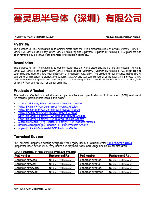
• Spartan-IIE Family FPGA Commercial Products Affected • Virtex-E Family FPGA Commercial Products Affected • Virtex-EM Family FPGA Commercial Products Affected • Virtex-II Family FPGA Commercial Products Affected • EasyPath Virtex-II Family FPGA Ordering Products Affected • EasyPath Virtex-II Family FPGA Quoting Products Affected • Automotive Market (XA) Spartan-IIE Family FPGA Products Affected • Defense/Aerospace (XQ) Spartan-IIE FPGA Products Affected • Appendix A – All Commercial SCD Products Affected
FPGA可编程逻辑器件芯片XC7Z030-1FFG676C中文规格书

Serial Transceiver Channels by Device/PackageTable 1-3 lists the quantity of GTX serial transceiver channels for most of the Zynq-7000SoC devices. In all devices, a serial transceiver channel is one set of MGTRXP, MGTRXN, MGTTXP, and MGTTXN pins. The XC7Z012S and XC7Z015, in the CLG485 package, have four GTP serial transceiver channels.Table 1-4 shows the number of available SelectIO resources (SIO), the number of differential SIO pairs, and the number of available PS I/Os for each Zynq-7000SoC device/package combination. When applicable, it also lists the number of SIOs in the 3.3V-capablehigh-range (HR) banks and the number of 1.8V-capable high-performance (HP) banks.Vivado Design Suite report_ssn tool. See the Simultaneous Switching Outputs section of the 7Series FPGAs SelectIO Resources User Guide (UG471) [Ref 8] for more information.Table 1-3:Serial Transceiver Channels by Device/PackageDeviceGTX (or GTP) Channels by PackageCL/CLG225CL/CLG400CL/CLG484CL/CLG485FB/FBG/FBV484SBG/SBV485RB484FB/FBG/FBV676FF/FFG/FFV676RF/RFG676FF/FFG/FFV900RF900FF/FFG/FFV1156RF1156XC7Z007S ––––––XC7Z010XA7Z010––––––XC7Z012S – 4 (GTP)––––XC7Z015– 4 (GTP)––––XC7Z014S ––––––XC7Z020XA7Z020––––––XC7Z030––44––XA7Z030––4–––XC7Z035–––816–XC7Z045–––816–XC7Z100––––1616XQ7Z020––––––XQ7Z030––44––XQ7Z045–––816–XQ7Z100––––1616Table 1-4:Available SIO and PS I/O Pins by Device/Package CombinationDevice I/O PinsCL225CLG225CL400CLG400CL484CLG484CLG485FB484FBG484FBV484RB484SBG485SBV485FB676FBG676FBV676FF676FFG676FFV676RF676RFG676FF900FFG900FFV900RF900FF1156FFG1156FFV1156RF1156SIO PSI/OSIO PSI/OSIO PSI/OSIO PSI/OSIO PSI/OSIO PSI/OSIO PSI/OSIO PSI/O HR HP HR HP HR HP HR HP HR HP HR HP HR HP HR HPXC7Z007S User I/O540861000128––––––––––––––––––Differential270–480–––––––––––––––––––XC7Z010 XA7Z010User I/O540861000128––––––––––––––––––Differential270–480–––––––––––––––––––XC7Z012S User I/O––––––1500128–––––––––––––––Differential––––––720––––––––––––––––XC7Z015User I/O––––––1500128–––––––––––––––Differential––––––720––––––––––––––––XC7Z014S User I/O–––12501282000128–––––––––––––––Differential–––600–960––––––––––––––––XC7Z020 XA7Z020User I/O–––12501282000128–––––––––––––––Differential–––600–960––––––––––––––––XC7Z030User I/O–––––––––1006312850100128100150128––––––Differential–––––––––4829–2448–4872–––––––XA7Z030User I/O–––––––––10063128––––––––––––Differential–––––––––4829–––––––––––––XC7Z035User I/O–––––––––––––––100150128212150128–––Differential–––––––––––––––4872–10272––––XC7Z045User I/O–––––––––––––––100150128212150128–––Differential–––––––––––––––4872–10272––––XC7Z100User I/O––––––––––––––––––212150128250150128 Differential––––––––––––––––––10272–12072–XQ7Z020User I/O–––12501282000128–––––––––––––––Differential–––600–960––––––––––––––––XQ7Z030User I/O–––––––––10063128–––100150128––––––Differential–––––––––4829––––4872–––––––XQ7Z045User I/O–––––––––––––––100150128212150128–––Differential–––––––––––––––4872–10272––––XQ7Z100User I/O––––––––––––––––––212150128250150128 Differential––––––––––––––––––10272–12072–VRN(8)Multi-function N/A This pin is for the DCI voltage reference resistor of N transistor (per bank, to be pulled High with reference resistor).VRP(8)Multi-function N/A This pin is for the DCI voltage reference resistor of P transistor (per bank, to be pulled Low with reference resistor).DXP_0, DXN_0(9)Dedicated N/A Temperature-sensing diode pins (Anode: DXP; Cathode: DXN). The thermal diode is accessed by using the DXP and DXN pins in bank 0. When not used, tie to GND.To use the thermal diode an appropriate external thermal monitoring IC must be added.The recommended temperature monitoring solution for Zynq-7000SoC devices uses the temperature sensor in the XADC block.T0, T1, T2, or T3Multi-function N/A This pin belongs to the memory byte group 0-3.T0_DQS, T1_DQS,T2_DQS, or T3_DQS Multi-function Bidirectional The DDR DQS strobe pin that belongs to the memory byte group T0–T3.Table 1-5:Zynq-7000SoC Pin Definitions (Cont’d)Pin Name Type Direction DescriptionPackage Pin Compatible DevicesCL225/CLG2257Z007S7Z010CL400/CLG4007Z007S7Z0107Z014S7Z020CL484/CLG4847Z014S7Z020SB/SBG/SBV485 or7Z012S7Z0157Z030CL/CLG485FB/FBG/FBV484 or RB4847Z030FB/FBG/FBV676 or7Z0307Z0357Z045 FF/FFG/FFV676 or RF/RFG676FF/FFG/FFV900 or RF9007Z0357Z0457Z100FF/FFG/FFV1156 or RF11567Z100。
FPGA可编程逻辑器件芯片XCZU11EG-L2FFVB1517E中文规格书

Using the CoolRunner-II SMBus/I2C Port Expander Design
Start Condition
Both SCL and SDA remain high when the interface is inactive. The master signals the start condition by transitioning SDA from high to low while SCL is high (Figure 2). Once a start condition is recognized by the CPLD, an internal ‘start’ pulse is generated, and the state machine will begin.
Figure 2: Start Condition Initiated
Acknowledge
The acknowledge bit is sent every 9th bit, indicating receipt of each data byte. Each byte transferred effectively requires 9 bits. The master generates the 9th clock pulse, and the recipient pulls down SDA during the acknowledge pulse. This means that when the master is transmitting to the CPLD, the CPLD generates the acknowledge bit. When the CPLD is transmitting to the master, the master generates the acknowledge bit.
FPGA可编程逻辑器件芯片XC3SD1800A-4FGG676C中文规格书
occupied by the first module. Then, move the first module to the location of thesecond module. These steps can be done in XDC constraint file.•If there is no other location available to be used as a temporary location, use the reset_property command from Tcl command window on the first module before relocating the second module to this location. The reset_property commandcannot be done in XDC constraint file and must be called from the Tcl command file or typed directly into the Tcl Console.SimulationFor comprehensive information about Vivado simulation components, as well as information about using supported third-party tools, see the Vivado Design Suite User Guide: Logic Simulation (UG900) [Ref18].For information regarding simulating the example design, see Simulating the Example Design in Chapter5.PIPE Mode SimulationThe UltraScale Devices Gen3 Integrated Block for PCIe core supports the PIPE mode simulation where the PIPE interface of the core is connected to the PIPE interface of the link partner. This mode increases the simulation speed.Use the Enable External PIPE Interface option on the Basic page of the Customize IP dialog box to enable PIPE mode simulation in the current Vivado Design Suite solution example design, in either Endpoint mode or Root Port mode. The External PIPE Interface signals are generated at the core boundary for access to the external device. Enabling this feature also provides the necessary hooks to use third-party PCI Express VIPs/BFMs instead of the Root Port model provided with the example design.For details, see Enable External PIPE Interface, page209.Table4-11 and Table4-12 describe the PIPE bus signals available at the top level of the core and their corresponding mapping inside the EP core (pcie_top) PIPE signals.Post-Synthesis/Post-Implementation Netlist SimulationThe UltraScale Devices Gen3 Integrated Block for PCIe core supports post-synthesis/post-implementation netlist functional simulations. However, some configurations do not support this feature in this release. See Table 4-13 for the configuration support of netlist functional simulations.Note:Post-synthesis/implementation netlist timing simulations are not supported for any of the configurations this release.Table 4-11:Common In/Out Commands and Endpoint PIPE Signals Mappings In Commands Endpoint PIPE Signals MappingOut Commands Endpoint PIPE Signals Mapping common_commands_in[25:0]not used common_commands_out[0]pipe_clk (1)common_commands_out[2:1]pipe_tx_rate_gt (2)common_commands_out[3]pipe_tx_rcvr_det_gt common_commands_out[6:4]pipe_tx_margin_gt common_commands_out[7]pipe_tx_swing_gt common_commands_out[8]pipe_tx_reset_gt common_commands_out[9]pipe_tx_deemph_gt common_commands_out[16:10]not used (3)Notes:1.pipe_clk is an output clock based on the core configuration. For Gen1 rate, pipe_clk is 125 MHz. For Gen2 and Gen3,pipe_clk is 250 MHz.2.pipe_tx_rate_gt indicates the pipe rate (2’b00-Gen1, 2’b01-Gen2 and 2’b10-Gen3).3.This ports functionality has been deprecated and can be left unconnected.Table 4-12:Input/Output Buses With Endpoint PIPE Signals MappingInput Bus Endpoint PIPE Signals MappingOutput Bus Endpoint PIPE Signals Mapping pipe_rx_0_sigs[31:0]pipe_rx0_data_gtpipe_tx_0_sigs[31: 0]pipe_tx0_data_gt pipe_rx_0_sigs[33:32]pipe_rx0_char_is_k_gtpipe_tx_0_sigs[33:32]pipe_tx0_char_is_k_gt pipe_rx_0_sigs[34]pipe_rx0_elec_idle_gtpipe_tx_0_sigs[34]pipe_tx0_elec_idle_gt pipe_rx_0_sigs[35]pipe_rx0_data_valid_gtpipe_tx_0_sigs[35]pipe_tx0_data_valid_gt pipe_rx_0_sigs[36]pipe_rx0_start_block_gtpipe_tx_0_sigs[36]pipe_tx0_start_block_gt pipe_rx_0_sigs[38:37]pipe_rx0_syncheader_gtpipe_tx_0_sigs[38:37]pipe_tx0_syncheader_gt pipe_rx_0_sigs[83:39]not used pipe_tx_0_sigs[39]pipe_tx0_polarity_gt pipe_tx_0_sigs[41:40]pipe_tx0_powerdown_gt pipe_tx_0_sigs[69:42]not used (1)Notes:1.This ports functionality has been deprecated and can be left unconnected.Post-Synthesis Netlist Functional SimulationTo run a post-synthesis netlist functional simulation:1.Generate the core with required configuration2.Open the example design and run Synthesis3.After synthesis is completed, in the Flow Navigator, right-click the Run Simulation option and select Run Post-Synthesis Functional Simulation .Post-Implementation Netlist Functional SimulationTo run post-implementation netlist functional simulations:plete the above steps post-synthesis netlist function simulation.2.Run the implementation for the generated example design.3.After implementation is completed, in the Flow Navigator, right-click the Run Simulation option and select Run Post-Implementation Functional Simulation .Synthesis and ImplementationFor details about synthesis and implementation, see the Vivado Design Suite User Guide: Designing with IP (UG896) [Ref 14].For information regarding synthesizing and implementing the example design, see Synthesizing and Implementing the Example Design in Chapter 5.Table 4-13:Configuration Support for Functional Simulation Configuration VerilogVHDL External PIPE Interface Mode Shared Logic in Core Shared Logic in Example Design EndpointYes Yes (Except Tandem mode with External Startup Primitive selected)No Yes Yes Root Port Not Supported at this time。
FPGA可编程逻辑器件芯片XC2V1500-5FF1152C中文规格书
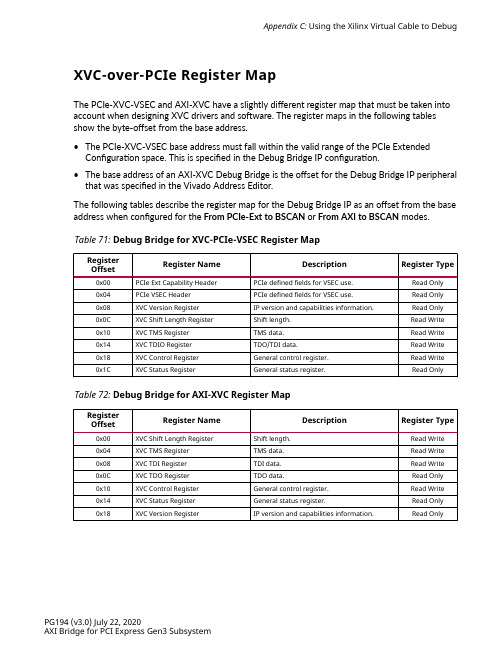
Appendix C: Using the Xilinx Virtual Cable to DebugXVC-over-PCIe Register MapThe PCIe-XVC-VSEC and AXI-XVC have a slightly different register map that must be taken into account when designing XVC drivers and software. The register maps in the following tablesshow the byte-offset from the base address.•The PCIe-XVC-VSEC base address must fall within the valid range of the PCIe Extended Configuration space. This is specified in the Debug Bridge IP configuration.•The base address of an AXI-XVC Debug Bridge is the offset for the Debug Bridge IP peripheral that was specified in the Vivado Address Editor.The following tables describe the register map for the Debug Bridge IP as an offset from the base address when configured for the From PCIe-Ext to BSCAN or From AXI to BSCAN modes.Table 71: Debug Bridge for XVC-PCIe-VSEC Register MapRegisterOffset Register Name Description Register Type0x00PCIe Ext Capability Header PCIe defined fields for VSEC use.Read Only0x04PCIe VSEC Header PCIe defined fields for VSEC use.Read Only0x08XVC Version Register IP version and capabilities information.Read Only0x0C XVC Shift Length Register Shift length.Read Write0x10XVC TMS Register TMS data.Read Write0x14XVC TDIO Register TDO/TDI data.Read Write0x18XVC Control Register General control register.Read Write0x1C XVC Status Register General status register.Read Only Table 72: Debug Bridge for AXI-XVC Register MapRegisterOffset Register Name Description Register Type0x00XVC Shift Length Register Shift length.Read Write0x04XVC TMS Register TMS data.Read Write0x08XVC TDI Register TDI data.Read Write0x0C XVC TDO Register TDO data.Read Only0x10XVC Control Register General control register.Read Write0x14XVC Status Register General status register.Read Only0x18XVC Version Register IP version and capabilities information.Read OnlyPG194 (v3.0) July 22, 2020AXI Bridge for PCI Express Gen3 SubsystemPCIe Ext Capability HeaderThis register is used to identify the PCIe-XVC-VSEC added to a PCIe design. The fields and values in the PCIe Ext Capability Header are defined by PCI-SIG and are used to identify the format of the extended capability and provide a pointer to the next extended capability, if applicable. When used as a PCIe-XVC-VSEC, the appropriate PCIe ID fields should be evaluated prior to interpretation. These can include PCIe Vendor ID, PCIe Device ID, PCIe Revision ID, Subsystem Vendor ID, and Subsystem ID. The provided drivers specifically check for a PCIe Vendor ID that matches Xilinx (0x10EE) before interpreting this register. The following table describes the fields within this register.Table 73: PCIe Ext Capability Header Register DescriptionBitLocation Field Description InitialValue Type15:0PCIeExtendedCapabilityIDThis field is a PCI-SIG defined ID number that indicates the natureand format of the Extended Capability. The Extended Capability IDfor a VSEC is 0x000B0x000B Read Only19:16CapabilityVersion This field is a PCI-SIG defined version number that indicates theversion of the capability structure present. Must be 0x1 for thisversion of the specification.0x1Read Only31:20NextCapabilityOffsetThis field is passed in from the user and contains the offset to thenext PCI Express Capability structure or 0x000 if no other itemsexist in the linked list of capabilities. For Extended Capabilitiesimplemented in the PCIe extended configuration space, this valuemust always be within the valid range of the PCIe ExtendedConfiguration space.0x000Read OnlyPCIe VSEC Header (PCIe-XVC-VSEC only)This register is used to identify the PCIe-XVC-VSEC when the Debug Bridge IP is in this mode. The fields are defined by PCI-SIG, but the values are specific to the Vendor ID (0x10EE for Xilinx). The PCIe Ext Capability Header register values should be qualified prior to interpreting this register.Table 74: PCIe XVC VSEC Header Register DescriptionBitLocation Field Description InitialValue Type15:0VSEC ID This field is the ID value that can be used to identify the PCIe-XVC-VSEC and is specific to the Vendor ID (0x10EE for Xilinx).0x0008Read Only19:16VSEC Rev This field is the Revision ID value that can be used to identify thePCIe-XVC-VSEC revision.0x0Read Only31:20VSECLength This field indicates the number of bytes in the entire PCIe-XVC-VSEC structure, including the PCIe Ext Capability Header and PCIeVSEC Header registers.0x020Read OnlyAppendix C: Using the Xilinx Virtual Cable to DebugPG194 (v3.0) July 22, 2020AXI Bridge for PCI Express Gen3 SubsystemAppendix C: Using the Xilinx Virtual Cable to DebugXVC Version Register (PCIe-XVC-VSEC only)This register is populated by the Xilinx tools and is used by the Vivado Design Suite to identifythe specific features of the Debug Bridge IP that is implemented in the hardware design.XVC Shift Length RegisterThis register is used to set the scan chain shift length within the debug scan chain.XVC TMS RegisterThis register is used to set the TMS data within the debug scan chain.XVC TDO/TDI Data Register(s)This register is used for TDO/TDI data access. When using PCIePCI-XVC-VSEC, these tworegisters are combined into a single field. When using AXI-XVC, these are implemented as twoseparate registers.XVC Control RegisterThis register is used for XVC control data.XVC Status RegisterThis register is used for XVC status information.XVC Driver and SoftwareExample XVC driver and software has been provided with the Vivado Design Suite installation, which is available at the following location:<Vivado_Installation_Path>/data/xicom/ driver/pcie/xvc_pcie.zip. This should be used for reference when integrating the XVCcapability into Xilinx FPGA platform design drivers and software. The provided Linux kernel mode driver and software implement XVC-over-PCIe debug for both PCIe-XVC-VSEC and AXI-XVCdebug bridge implementations.When operating in PCIe-XVC-VSEC mode, the driver will initiate PCIe configuration transactions to interface with the FPGA debug network. When operating in AXI-XVC mode, the driver willinitiate 32-bit PCIe Memory BAR transactions to interface with the FPGA debug network. Bydefault, the driver will attempt to discover the PCIe-XVC-VSEC and use AXI-XVC if the PCIe-XVC-VSEC is not found in the PCIe configuration extended capability linked list.PG194 (v3.0) July 22, 2020AXI Bridge for PCI Express Gen3 Subsystem。
FPGA可编程逻辑器件芯片XCZU11EG-L2FFVC1760E中文规格书
Module 1:Introduction and Ordering InformationDS099 (v3.1) June 27, 2013•Introduction •Features•Architectural Overview •Array Sizes and Resources •User I/O Chart •Ordering InformationModule 2: Functional DescriptionDS099 (v3.1) June 27, 2013•Input/Output Blocks (IOBs)•IOB Overview•SelectIO™ Interface I/O Standards•Configurable Logic Blocks (CLBs)•Block RAM •Dedicated Multipliers•Digital Clock Manager (DCM)•Clock Network •ConfigurationModule 3:DC and Switching CharacteristicsDS099 (v3.1) June 27, 2013•DC Electrical Characteristics •Absolute Maximum Ratings •Supply Voltage Specifications •Recommended Operating Conditions •DC Characteristics •Switching Characteristics•I/O Timing•Internal Logic Timing •DCM Timing•Configuration and JT AG TimingModule 4: Pinout DescriptionsDS099 (v3.1) June 27, 2013•Pin Descriptions •Pin Behavior During Configuration •Package Overview •Pinout T ables •FootprintsDS099 June 27, 2013Product SpecificationParallel Configuration Modes (SelectMAP)This section describes the dual-purpose configuration pins used during the Master and Slave Parallel configuration modes,sometimes also called the SelectMAP modes. In both Master and Slave Parallel configuration modes, D0-D7 form the byte-wide configuration data input. See Table 75 for Mode Select pin settings required for Parallel modes.As shown in Figure 41, D0 is the most-significant bit while D7 is the least-significant bit. Bits D0-D3 form the high nibble of the byte and bits D4-D7 form the low nibble.In the Parallel configuration modes, both the VCCO_4 and VCCO_5 voltage supplies are required and must both equal the voltage of the attached configuration device, typically either 2.5V or 3.3V .Assert Low both the chip-select pin, CS_B, and the read/write control pin, RDWR_B, to write the configuration data byte presented on the D0-D7 pins to the FPGA on a rising-edge of the configuration clock, CCLK. The order of CS_B and RDWR_B does not matter, although RDWR_B must be asserted throughout the configuration process. If RDWR_B is de-asserted during configuration, the FPGA aborts the configuration operation.After configuration, these pins are available as general-purpose user I/O. However, the SelectMAP configuration interface is optionally available for debugging and dynamic reconfiguration. T o use these SelectMAP pins after configuration, set the Persist bitstream generation option.The Readback debugging option, for example, requires the Persist bitstream generation option. During Readback mode, assert CS_B Low, along with RDWR_B High, to read a configuration data byte from the FPGA to the D0-D7 bus on a rising CCLK edge. During Readback mode, D0-D7 are output pins.In all the cases, the configuration data and control signals are synchronized to the rising edge of the CCLK clock signal.Table 71:Dual-Purpose Pins Used in Master or Slave Serial ModePin Name Direction DescriptionDINInputSerial Data Input:During the Master or Slave Serial configuration modes, DIN is the serial configuration data input, and all data is synchronized to the rising CCLK edge. After configuration, this pin is available as a user I/O. This signal is located in Bank 4 and its output voltage determined by VCCO_4.The BitGen option Persist permits this pin to retain its configuration function in the User mode.DOUT OutputSerial Data Output:In a multi-FPGA design where all the FPGAs use serial mode, connect the DOUT output of one FPGA—in either Master or Slave Serial mode—to the DIN input of the next FPGA—in Slave Serial mode—so that configuration data passes from one to the next, in daisy-chain fashion. This “daisy chain” permits sequential configuration of multiple FPGAs.This signal is located in Bank 4 and its output voltage determined by VCCO_4.The BitGen option Persist permits this pin to retain its configuration function in the User mode.INIT_BBidirectional (open-drain)Initializing Configuration Memory/Configuration Error:Just after power is applied, the FPGA produces a Low-to-High transition on this pin indicating that initialization (i.e., clearing) of the configuration memory has finished. Before entering the User mode, this pin functions as an open-drain output, which requires a pull-up resistor in order to produce a High logic level. In a multi-FPGA design, tie (wire AND) the INIT_B pins from all FPGAs together so that the common node transitions High only after all of the FPGAs have been successfully initialized.Externally holding this pin Low beyond the initialization phase delays the start of configuration. This action stalls the FPGA at the configuration step just before the mode select pins are sampled.During configuration, the FPGA indicates the occurrence of a data (i.e., CRC) error by asserting INIT_B Low.This signal is located in Bank 4 and its output voltage determined by VCCO_4.The BitGen option Persist permits this pin to retain its configuration function in the User mode.I/O Bank 4 (VCCO_4)I/O Bank 5 (VCCO_5)High NibbleLow Nibble Configuration Data ByteD0D1D2D3D4D5D6D70xFC =1111110(MSB)(LSB)Figure 41:Configuration Data Byte Mapping to D0-D7 BitsHSWAP_EN: Disable Pull-up Resistors During ConfigurationAs shown in Table 76, a Low on this asynchronous pin enables pull-up resistors on all user I/Os not actively involved in the configuration process, although only until device configuration completes. A High disables the pull-up resistors during configuration, which is the desired state for some applications.The dedicated configuration CONFIG pins (CCLK, DONE, PROG_B, HSWAP_EN, M2, M1, M0), the JTAG pins (TDI, TMS, TCK, TDO) and the INIT_B always have active pull-up resistors during configuration, regardless of the value on HSWAP_EN.After configuration, HSWAP_EN becomes a "don’t care" input and any pull-up resistors previously enabled by HSWAP_EN are disabled. If a user I/O in the application requires a pull-up resistor after configuration, place a PULLUP primitive on the associated I/O pin or, for some pins, set the associated bitstream generator option.The Bitstream generator option HswapenPin determines whether a pull-up resistor to VCCAUX, a pull-down resistor, or no resistor is present on HSWAP_EN after configuration.JTAG: Dedicated JTAG Port PinsThese pins are dedicated connections to the four-wire IEEE 1532/IEEE 1149.1 JT AG port, shown in Figure 43 anddescribed in T able 77. The JTAG port is used for boundary-scan testing, device configuration, application debugging, and possibly an additional serial port for the application. These pins are dedicated and are not available as user-I/O pins. Every package has four dedicated JT AG pins and these pins are powered by the +2.5V VCCAUX supply.For additional information on JTAG configuration, see Boundary-Scan (JTAG) Mode, page 50.Table 76:HSWAP_EN EncodingHSWAP_EN FunctionDuring Configuration0Enable pull-up resistors on all pins not actively involved in the configuration process. Pull-ups are only active until configuration completes. See T able 79.1No pull-up resistors during configuration.After Configuration, User ModeXThis pin has no function except during device configuration.Notes:1.X =don’t care, either 0 or 1.Table 77:JTAG Pin DescriptionsPin Name Direction Description Bitstream Generation OptionTCKInputTest Clock: The TCK clock signal synchronizes all boundary scan operations on its rising edge.The BitGen option TckPin determines whether a pull-up resistor, pull-downresistor or no resistor is present.TDI InputTest Data Input: TDI is the serial data input for all JT AG instruction and data registers. This input is sampled on the rising edge of TCK.The BitGen option TdiPin determines whether a pull-up resistor, pull-down resistor or no resistor is present.TMS InputTest Mode Select: The TMS input controls the sequence of states through which the JTAG T AP state machine passes. This input is sampled on the rising edge of TCK.The BitGen option TmsPin determines whether a pull-up resistor, pull-down resistor or no resistor is present.TDO OutputTest Data Output: The TDO pin is the data output for all JT AG instruction and data registers. This output is sampled on the rising edge of TCK. The TDO output is an active totem-pole driver and is not like the open-collector TDO output on Virtex ®-II Pro FPGAs.The BitGen option TdoPin determines whether a pull-up resistor, pull-down resistor or no resistor is present.All VCCAUX inputs must be connected together and to the +2.5V voltage supply. Furthermore, there must be sufficient supply decoupling to guarantee problem-free operation, as described in XAPP623.Because VCCAUX connects to the DCMs and the DCMs are sensitive to voltage changes, be sure that the VCCAUX supply and the ground return paths are designed for low noise and low voltage drop, especially that caused by a large number of simultaneous switching I/Os.GND Type: GroundAll GND pins must be connected and have a low resistance path back to the various VCCO, VCCINT, and VCCAUX supplies.Pin Behavior During ConfigurationTable79 shows how various pins behave during the FPGA configuration process. The actual behavior depends on the values applied to the M2, M1, and M0 mode select pins and the HSWAP_EN pin. The mode select pins determine which of the DUAL type pins are active during configuration. In JT AG configuration mode, none of the DUAL-type pins are used for configuration and all behave as user-I/O pins.All DUAL-type pins not actively used during configuration and all I/O-type, DCI-type, VREF-type, GCLK-type pins are high impedance (floating, three-stated, Hi-Z) during the configuration process. These pins are indicated in Table79 as shaded table entries or cells. These pins have a pull-up resistor to their associated VCCO if the HSWAP_EN pin is Low. When HSWAP_EN is High, these pull-up resistors are disabled during configuration.Some pins always have an active pull-up resistor during configuration, regardless of the value applied to the HSWAP_EN pin. After configuration, these pull-up resistors are controlled by Bitstream Options.•All the dedicated CONFIG-type configuration pins (CCLK, PROG_B, DONE, M2, M1, M0, and HSWAP_EN) have a pull-up resistor to VCCAUX.•All JTAG-type pins (TCK, TDI, TMS, TDO) have a pull-up resistor to VCCAUX.•The INIT_B DUAL-purpose pin has a pull-up resistor to VCCO_4 or VCCO_BOTTOM, depending on package style. After configuration completes, some pins have optional behavior controlled by the configuration bitstream loaded into the part. For example, via the bitstream, all unused I/O pins can be collectively configured as input pins with either a pull-up resistor, a pull-down resistor, or be left in a high-impedance state.Table 79:Pin Behavior After Power-Up, During ConfigurationPin NameConfiguration Mode Settings <M2:M1:M0>BitstreamConfigurationOption Serial Modes SelectMap Parallel Modes JTAG Mode<1:0:1>Master <0:0:0>Slave <1:1:1>Master <0:1:1>Slave <1:1:0>I/O: General-purpose I/O pinsIO UnusedPinIO_Lxxy_#UnusedPin DUAL: Dual-purpose configuration pinsIO_Lxxy_#/DIN/D0DIN (I)DIN (I)D0 (I/O)D0 (I/O)Persist UnusedPinIO_Lxxy_#/D1D1 (I/O)D1 (I/O)Persist UnusedPinIO_Lxxy_#/D2D2 (I/O)D2 (I/O)Persist UnusedPinIO_Lxxy_#/D3D3 (I/O)D3 (I/O)Persist UnusedPinIO_Lxxy_#/D4D4 (I/O)D4 (I/O)Persist UnusedPin。
FPGA可编程逻辑器件芯片EP4CE22F17C7N中文规格书
Arria II Device Architecture ■Diagnostic features■Serial loopback from the transmitter serializer to the receiver CDR fortransceiver physical coding sublayer (PCS) and PMA diagnostics■Parallel loopback from the transmitter PCS to the receiver PCS with built-in selftest (BIST) pattern generator and verifier■Reverse serial loopback pre- and post-CDR to transmitter buffer for physicallink diagnostics■Loopback master and slave capability in PCIe hard IP blocks■Support for protocol features such as MSB-to-LSB transmission in aSONET/SDH configuration and spread-spectrum clocking in a PCIeconfiguration Table 1–5 lists common protocols and the Arria II dedicated circuitry and features forimplementing these protocols.1For other protocols supported by Arria II devices, such as SONET/SDH, SDI, SATAand SRIO, refer to the Transceiver Architecture in Arria II Devices chapter.Table 1–5.Sample of Supported Protocols and Feature Descriptions for Arria II Devices Supported ProtocolsFeature Descriptions PCIe ■Complete PCIe Gen1 and Gen2 protocol stack solution compliant to PCIe BaseSpecification 2.0 that includes PHY/MAC, Data Link, and Transaction layer circuitryembedded in the PCIe hard IP blocks.■PCIe Gen1 has x1, x2, x4, and x8 lane configurations. PCIe Gen2 has x1, x2, and x4 laneconfigurations. PCIe Gen2 does not support x8 lane configurations■Built-in circuitry for electrical idle generation and detection, receiver detect, power statetransitions, lane reversal, and polarity inversion■8B/10B encoder and decoder, receiver synchronization state machine, and ±300 partsper million (PPM) clock compensation circuitry■Options to use:■Hard IP Data Link Layer and Transaction Layer ■Hard IP Data Link Layer and custom Soft IP Transaction LayerXAUI/HiGig/HiGig+ ■Compliant to IEEE P802.3ae specification ■Embedded state machine circuitry to convert XGMII idle code groups (||I||) to and from idle ordered sets (||A||, ||K||, ||R||) at the transmitter and receiver, respectively■8B/10B encoder and decoder, receiver synchronization state machine, lane deskew, and±100 PPM clock compensation circuitryGbE ■Compliant to IEEE 802.3 specification■Automatic idle ordered set (/I1/, /I2/) generation at the transmitter, depending on thecurrent running disparity■8B/10B encoder and decoder, receiver synchronization state machine, and ±100 PPMclock compensation circuitryCPRI/OBSAI ■Transmit bit slipper eliminates latency uncertainty to comply with CPRI/OBSAIspecifications■Optimized for power and cost for remote radio heads and RF modulesDocument Revision HistoryAdaptive Logic ModulesNormal ModeNormal mode is suitable for general logic applications and combinational functions.In this mode, up to eight data inputs from the LAB local interconnect are inputs to thecombinational logic. Normal mode allows two functions to be implemented in oneArria II ALM, or a single function of up to six inputs. The ALM can support certaincombinations of completely independent functions and various combinations offunctions that have common inputs.Figure2–7 shows the supported LUT combinations in normal mode.Figure2–7.ALM in Normal Mode (Note1)Note to Figure2–7:(1)Combinations of functions with fewer inputs than those shown are also supported. For example, combinations of functions with the followingnumber of inputs are supported: 4 and 3, 3 and 3, 3 and 2, and 5 and 2.Normal mode provides complete backward-compatibility with 4-input LUTarchitectures.。
FPGA可编程逻辑器件芯片XC3S2000-4FGG676C中文规格书
Adaptable Engines in PLThe PL Adaptable Engines are building blocks to instantiate functional units in the PL and they include:•Digital signal processing engine (DSP)•Configurable logic blocks (CLB): logic and LUT•Block RAM: 4 KB data with ECC (36 Kb)•UltraRAM: 32 KB data with ECC (288 Kb)Digital Signal Processing EngineVersal devices have many dedicated low-power DSPs combining high speed with small size while retaining system design flexibility. The DSP resources enhance the speed and efficiency of many applications beyond digital signal processing such as wide dynamic bus shifters, memory address generators, wide bus multiplexers, and memory-mapped I/O registers. The DSP engine is defined using the Xilinx DSP58 primitive.For more information, see Versal ACAP DSP Engine Architecture Manual (AM004).Configurable Logic BlockThe configurable logic block (CLB) includes logic and look-up tables (LUTs) that can be configured into many different combinations and connected to other components in the PL to create special purpose functions, processing units, and other entities.Every CLB contains 32 LUTs and 64 flip-flops. The LUTs can be configured as either one 6-input LUT with one output, or as two 5-input LUTs with separate outputs but common inputs. EachLUT output can optionally be registered in a flip-flop.In addition to the LUTs and flip-flops, the CLB contains arithmetic carry logic and multiplexers to create wider logic functions. Within each CLB, 16 LUTs can be configured as 64-bit RAM, 32-bit shift registers (SRL32), or two SRL16s.Within every CLB are dedicated interconnect paths for connecting LUTs without having to exit and re-enter a CLB, drastically reducing the use of global routing resources. In addition, new CLB features such as cascade multiplexers allow flexible carry logic structures to be created.For more information, see the Versal ACAP Configurable Logic Block Architecture Manual (AM005).Figure 10: PL System PerspectiveIn addition to the PL interconnect interfaces shown in the figure, the PL port interface signals include the system interrupts, errors, events, and other signals from all parts of the device.Section II: Hardware ArchitectureChapter 9: Programmable LogicBlock RAMThe dual-port block RAMs have 4 KB of data storage capacity that is protected by error correction coding (ECC) for a total of 36 Kb per block RAM. The RAM can be configured as either one 36 Kb RAM, or two completely independent 18 Kb RAMs. The RAMs can be configured to operate in simple dual port mode (one read-only port and one write-only port) or true dual port mode (both ports have read and write interfaces). The block RAM can also be configure for single port mode. Each port has its own clock and address interface. The ports can be configured independently as 4K×9, 2K×18, 1K×36, or 512×72. The 512×72 mode requires simple dual port mode.The block RAM is described in the Versal ACAP Memory Resources Architecture Manual (AM007).UltraRAMThe dual-port block RAMs have 32 KB of data storage capacity that is protected by error correction coding (ECC) for a total of 288 Kb per block RAM. Each port can be configured independently as 32K×9, 16K×18, 8K×36, or 4K×72.•Cascade-able for building larger memories: dedicated column routing wires to connect adjacent units•ECC on both ports with single bit error detection and correction, and double bit error detection•Sleep power saving featuresThe UltraRAM is described in the Versal ACAP Memory Resources Architecture Manual (AM007).。
FPGA可编程逻辑器件芯片XC2V1000-4FG256C中文规格书
AXI4 Memory Mapped with PCIe to AXI4-Lite Master and PCIe to DMA Bypass Example DesignThe following figure shows a system where the PCIe to AXI4-Lite Master (BAR0) and PCIe to DMA Bypass (BAR2) are selected. 4K block RAM is connected to the PCIe to DMA Bypass interfaces. The host can use DMA Bypass interface to read/write data to the user space using the AXI4 MM interface. This interface bypasses DMA engines. The host can also use the PCIe to AXI4-Lite Master (BAR0 address space) to write/read user logic. The example design connects 4K block RAM to the PCIe to AXI4-Lite Master interface so the user application can perform read/writes.Figure 22: AXI-MM Example with PCIe to DMA Bypass Interface and PCIe to AXI-LiteMaster Enabled*may include wrapper as necessaryX15047-010115AXI4 Memory Mapped with AXI4-Lite Slave Interface Example DesignWhen the PCIe® to AXI4-Lite master and AXI4-Lite slave interface are enabled, the generated example design (shown in the following figure) has a loopback from AXI4-Lite master to AXI4-Lite slave. Typically, the user logic can use a AXI4-Lite slave interface to read/write DMA/Bridge Subsystem for PCI Express® registers. With this example design, the host can use PCIe to AXI4-Lite Master (BAR0 address space) and read/write DMA/Bridge Subsystem for PCI Express®registers, which is the same as using PCIe to DMA (BAR1 address space). This example design also shows PCIe to DMA bypass Interface (BAR2) enabled.Figure 23: AXI-MM Example with AXI-Lite Slave Enabled*may include wrapper as necessaryX15045-010115Chapter 6: Example DesignAXI4-Stream Example DesignWhen the AXI4-Stream interface is enabled, each H2C streaming channels is looped back to C2H channel. As shown in the following figure, the example design gives a loopback design for AXI4 streaming. The limitation is that you need to select an equal number of H2C and C2H channels for proper operation. This example design also shows PCIe to DMA bypass interface and PCIe to AXI-Lite Master selected.Figure 24: AXI4-Stream Example with PCIe to DMA Bypass Interface and PCIe to AXI-Lite Master EnabledX15046-010115。
FPGA可编程逻辑器件芯片XC2V1000-4FF1152C中文规格书
Table 34: Configuration Management Interface PortsPort Direction Width Descriptioncfg_mgmt_addr I19Read/Write Address.Configuration Space Dword-aligned addresscfg_mgmt_byte_enable I4Byte EnableByte Enable for write data, where cfg_mgmt_byte_enable[0]corresponds to cfg_mgmt_write_data[7:0] and so oncfg_mgmt_read_data O32Read Data OutRead data provides the configuration of the Configuration andManagement registerscfg_mgmt_read I1Read EnableAsserted for a read operation. Active-Highcfg_mgmt_read_write_done O1Read/Write Operation CompleteAsserted for 1 cycle when operation is complete. Active-High cfg_mgmt_write_data I32Write dataWrite data is used to configure the Configuration andManagement registerscfg_mgmt_write I1Write EnableAsserted for a write operation. Active-High Descriptor Bypass ModeIf in the PCIe DMA Tab in the Vivado IDE either Descriptor Bypass for Read (H2C) or Descriptor Bypass for Write (C2H) are selected, these ports are present. Each binary bit corresponds to a channel: LSB correspond to Channel 0. Value 1 in bit positions means the corresponding channel descriptor bypass is enabled.Table 35: H2C 0-3 Descriptor Bypass PortPort Direction Descriptionh2c_dsc_byp_ready O Channel is ready to accept new descriptors. Afterh2c_dsc_byp_ready is deasserted, one additional descriptorcan be written. The Control register 'Run' bit must beasserted before the channel accepts descriptors.h2c_dsc_byp_load I Write the descriptor presented at h2c_dsc_byp_data into thechannel’s descriptor buffer.h2c_dsc_byp_src_addr[63:0]I Descriptor source address to be loaded.h2c_dsc_byp_dst_addr[63:0]I Descriptor destination address to be loaded.h2c_dsc_byp_len[27:0]I Descriptor length to be loaded.h2c_dsc_byp_ctl[15:0]I Descriptor control to be loaded.[0]: Stop. Set to 1 to stop fetching next descriptor.[1]: Completed. Set to 1 to interrupt after the engine hascompleted this descriptor.[3:2]: Reserved.[4]: EOP. End of Packet for AXI-Stream interface.[15:5]: Reserved.All reserved bits can be forced to 0s.Table 36: C2H 0-3 Descriptor Bypass PortsPort Direction Descriptionc2h_dsc_byp_ready O Channel is ready to accept new descriptors. Afterc2h_dsc_byp_ready is deasserted, one additional descriptorcan be written. The Control register 'Run' bit must beasserted before the channel accepts descriptors.c2h_dsc_byp_load I Descriptor presented at c2h_dsc_byp_* is valid.c2h_dsc_byp_src_addr[63:0]I Descriptor source address to be loaded.c2h_dsc_byp_dst_addr[63:0]I Descriptor destination address to be loaded.c2h_dsc_byp_len[27:0]I Descriptor length to be loaded.c2h_dsc_byp_ctl[15:0]I Descriptor control to be loaded.[0]: Stop. Set to 1 to stop fetching next descriptor.[1]: Completed. Set to 1 to interrupt after the engine hascompleted this descriptor.[3:2]: Reserved.[4]: EOP. End of Packet for AXI-Stream interface.[15:5]: Reserved.All reserved bits can be forced to 0s.The following timing diagram shows how to input the descriptor in descriptor bypass mode. When dsc_byp_ready is asserted, a new descriptor can be pushed in with thedsc_byp_load signal.Figure 8: Timing Diagram for Descriptor Bypass ModeIMPORTANT! Immediately after dsc_byp_ready is deasserted, one more descriptor can be pushed in.In the above timing diagram, a descriptor is pushed in when dsc_byp_ready is deasserted. Related InformationPCIe DMA TabRegister SpaceNote: This document covers only DMA mode register space. For AXI Bridge mode, see the AXI Bridge forPCI Express Gen3 Subsystem Product Guide (PG194).Configuration and status registers internal to the DMA/Bridge Subsystem for PCI Express® and those in the user logic can be accessed from the host through mapping the read or write request to a Base Address Register (BAR). Based on the BAR hit, the request is routed to the appropriate location. For PCIe BAR assignments, see Target Bridge.PCIe to AXI Bridge Master Address MapTransactions that hit the PCIe to AXI Bridge Master are routed to the AXI4 Memory Mapped user interface.PCIe to DMA Address MapTransactions that hit the PCIe to DMA space are routed to the DMA Subsystem for thePCIeDMA/Bridge Subsystem for PCI Express® internal configuration register bus. This bussupports 32 bits of address space and 32-bit read and write requests.DMA/Bridge Subsystem for PCIe registers can be accessed from the host or from the AXI Slave interface. These registers should be used for programming the DMA and checking status.PCIe to DMA Address FormatTable 37: PCIe to DMA Address Format31:1615:1211:87:0Reserved Target Channel Byte Offset Table 38: PCIe to DMA Address Field DescriptionsBit Index Field Description15:12Target The destination submodule within the DMA4’h0: H2C Channels4’h1: C2H Channels4’h2: IRQ Block4’h3: Config4’h4: H2C SGDMA4’h5: C2H SGDMA4’h6: SGDMA Common4'h8: MSI-XChapter 3: Product Specification。
- 1、下载文档前请自行甄别文档内容的完整性,平台不提供额外的编辑、内容补充、找答案等附加服务。
- 2、"仅部分预览"的文档,不可在线预览部分如存在完整性等问题,可反馈申请退款(可完整预览的文档不适用该条件!)。
- 3、如文档侵犯您的权益,请联系客服反馈,我们会尽快为您处理(人工客服工作时间:9:00-18:30)。
Receiver PLL Divider Limitations
Table 5 defines supported receiver PLL divider combinations.
Table 5: Supported Receiver PLL Divider Combinations
Receiver Mode
Configuration Guide for more information. 3. -12 is only available in C-grade devices. The XC4VFX140C is available in the -10 and -11 speed grades;
the XC4VFX140I is available only in the -10 speed grade.
Table 6: SYNCLK1OUT and SYNCLK2OUT to BUFG, PMCD, and DCM
Connection To
C-Grade
Maximum Frequency (MHz)
I-Grade
BUFG
375
312
DCM, PMCD
290
Not supported.
EN070 (v1.8) May 14, 2008
EN070 (v1.8) May 14, 2008
0 0 Errata Notification
Introduction
Thank you for designing with the Xilinx Virtex™-4 family of devices. Although Xilinx has made every effort to ensure the highest possible quality, the devices in Table 1 are subject to the limitations described in the following errata.
EN070 (v1.8) May 14, 2008
Errata Notification
Table 2: Digital Receiver Attributes
Attribute
Buffered Mode Value
RX_BUFFER_USE
TRUE
RXCLK0_FORCE_PMACLK
TRUE
DIGRX_SYNC_MODE
Notes:
1. For lower wide-band jitter generation, choose a reference clock frequency that uses a lower feedback divider. 2. Line Rate = VCO Frequency*2/TXOUTDIV2SEL. 3. Reference Clock = VCO Frequency/TXPLLNDIVSEL
5000
Reference Clock
The MGTCLK input pins in the -10 devices covered by this errata (Table 1) have a maximum frequency of 400 MHz and a minimum peak-to-peak differential input voltage of 250 mV. No such restrictions exist for -11 and -12 devices.
Xilinx recognizes the present level of RocketIO pin ESD is lower than Xilinx internal standards. Xilinx continues to evaluate ESD requirements for high-speed serial interconnects and is committed to providing best-in-class ESD.
Line Rate (Mb/s)
Minimum Maximum
Output Divider RXOUTDIV2SEL
4960
6500
1
2480
4300
2
Analog CDR
3100
4300
2
1250
2150
4
Digital CDR
622
1250
1
Notes:
1. Line Rate (Analog CDR) = VCO Frequency*2/RXOUTDIV2SEL 2. Line Rate (Digital CDR) = VCO Frequency*2/8 3. Reference Clock = VCO Frequency/RXPLLNDIVSEL
EN070 (v1.8) May 14, 2008
Errata Notification
RXSIGDET – Receive Out-of-Band (Receive OOB) Signaling
The RXCDRLOS attribute does not function with the resolution and accuracy stated in UG076:Virtex-4 RocketIO Multi-Gigabit Transceiver User Guide. Refer to Xilinx application note XAPP732: Inactive Transceiver Behavior Work-Arounds for Virtex-4 FX RocketIO MGTs for further details.
Feedback Divider RXPLLNDIVSEL
8, 10 8, 10 16, 20 8, 10, 16, 20 8, 10, 16, 20, 32, 40
VCO Frequency (MHz)
Minimum Maximum
2480
3250
2480
4300
3100
4300
2500
4300
2488
The CDM ESD for the RocketIO pins (TXN, TXP, RXN, RXP, AVCCAUXRX, GNDA, AVCCAUXTX, VTRX, VTTX, AVCCAUXMGT, MGTCLKP, and MGTCLKN) deviates from the product definition of 250V. The XC4VFX20 and XC4VFX60 devices meet a level of 150V. The XC4VFX100 device meets a level of 100V.
Table 4: Supported Transmitter PLL Divider Combinations
Line Rate (Mb/s)
Minimum Maximum
Output Divider TXOUTDIV2SEL
Feedback Divider TXPLLNDIVSEL
4960
6500
Step 0(1)
Devices
JTAG ID (Revision Code)(2)
XC4VFX20C
2
XC4VFX20I
NA
XC4VFX40C
NA
XC4VFX40I
NA
XC4VFX60C
2
XC4VFX60I
NA
XC4VFX100C
0
XC4VFX100I
NA
XC4VFX140C
NA
XC4VFX140I
1
8, 10
2480
4300
2
8, 10
3100
4300
2
16, 20
1240
2150
4
8, 10, 16, 20
622
1075
8
8, 10, 16, 20
VCO Frequency (MHz)
Minimum Maximum
2480
3250
2480
4300
3100
4300
2480
4300
2488
4300
SYNCLK1OUT and SYNCLK2OUT Ports
The GT11CLK output ports SYNCLK1OUT and SYNCLK2OUT to BUFG, PMCD, and DCM are supported in the devices covered by this errata (Table 1) as shown in Table 6:
The GREFCLK input port has a maximum frequency of 160 MHz (for all speed grades).
RXPCSHCLKOUT and TXPCSHCLKOUT Ports
The RXPCSHCLKOUT and TXPCSHCLKOUT MGT output clock ports are not supported in the devices covered by this errata (Table 1).
FALSE
See the "Digital Receiver" section of UG076: Virtex-4 RocketIO Multi-Gigabit Transceiver User Guide for more details regarding these attributes.