Processing of the fluxgate output signal
mcp6002
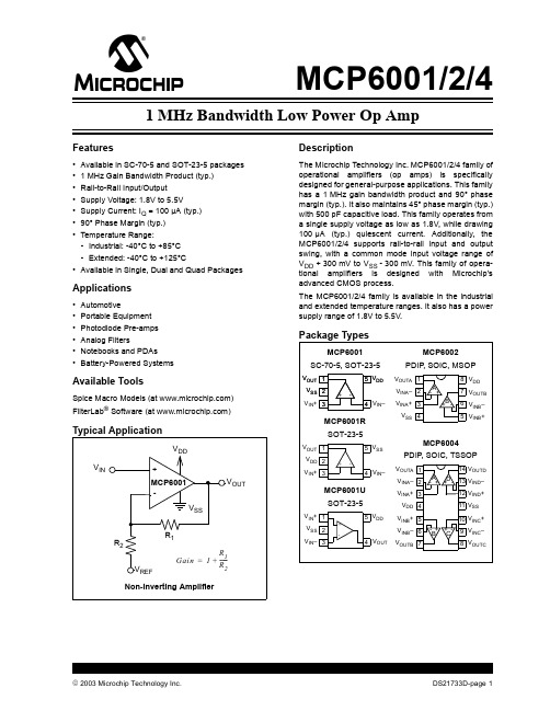
2003 Microchip Technology Inc.DS21733D-page 1MMCP6001/2/4Features•Available in SC-70-5 and SOT-23-5 packages •1MHz Gain Bandwidth Product (typ.)•Rail-to-Rail Input/Output•Supply Voltage: 1.8V to 5.5V•Supply Current: I Q = 100µA (typ.)•90° Phase Margin (typ.)•T emperature Range:-Industrial: -40°C to +85°C -Extended: -40°C to +125°C•Available in Single, Dual and Quad PackagesApplications•Automotive•Portable Equipment •Photodiode Pre-amps •Analog Filters•Notebooks and PDAs•Battery-Powered SystemsAvailable ToolsSpice Macro Models (at )FilterLab® Software (at )Typical ApplicationDescriptionThe Microchip Technology Inc. MCP6001/2/4 family of operational amplifiers (op amps) is specifically designed for general-purpose applications. This family has a 1MHz gain bandwidth product and 90° phase margin (typ.). It also maintains 45° phase margin (typ.)with 500pF capacitive load. This family operates from a single supply voltage as low as 1.8V, while drawing 100µA (typ.) quiescent current. Additionally, the MCP6001/2/4 supports rail-to-rail input and output swing, with a common mode input voltage range of V DD +300mV to V SS -300mV. This family of opera-tional amplifiers is designed with Microchip’s advanced CMOS process.The MCP6001/2/4 family is available in the industrial and extended temperature ranges. It also has a power supply range of 1.8V to 5.5V.Package TypesR 1V OUTR 2V INV DD+-Gain 1R 1R 2-----+=Non-Inverting AmplifierMCP6001V REFV SSMCP6001+V IN –V V IN +SC-70-5, SOT-23-5MCP6002PDIP , SOIC, MSOPMCP6004V INA +V INA –V SS 123414131211-V OUTA +-+AD V DD V OUTDV IND –V IND +1098567V OUTB V INB –V INB +V INC +V INC –V OUTC+-B C-+PDIP , SOIC, TSSOPV INA +V INA –V SS 12348765-V OUTA +-+A B V DD V OUTB V INB –V INB +4123-5V DDOUT V SS MCP6001R SOT-23-54123-+5V SSV IN –V OUT V DD V IN +MCP6001U SOT-23-54123-+5V DDV OUTV IN +V SS V IN –1MHz Bandwidth Low Power Op AmpMCP6001/2/4DS21733D-page 2 2003 Microchip Technology Inc.1.0ELECTRICALCHARACTERISTICSAbsolute Maximum Ratings †V DD - V SS .........................................................................7.0V All Inputs and Outputs ......................V SS -0.3V to V DD +0.3V Difference Input Voltage .......................................|V DD - V SS |Output Short Circuit Current ..................................continuous Current at Input Pins ....................................................±2mA Current at Output and Supply Pins ............................±30mA Storage Temperature....................................-65°C to +150°C Maximum Junction Temperature (T J )..........................+150°C ESD Protection On All Pins (HBM;MM)...............≥ 4kV; 200V † Notice: Stresses above those listed under “Maximum Rat-ings” may cause permanent damage to the device. This is a stress rating only and functional operation of the device at those or any other conditions above those indicated in the operational listings of this specification is not implied. Expo-sure to maximum rating conditions for extended periods may affect device reliability.PIN FUNCTION TABLEDC ELECTRICAL SPECIFICATIONSNameFunctionV IN +, V INA +, V INB +, V INC +, V IND +Non-inverting Inputs V IN –, V INA –, V INB –, V INC –, V IND –Inverting Inputs V DD Positive Power Supply V SSNegative Power Supply V OUT , V OUTA , V OUTB , V OUTC , V OUTDOutputsElectrical Characteristics : Unless otherwise indicated, T A = +25°C, V DD = +1.8V to +5.5V, V SS = GND, V CM = V DD /2, R L = 10k Ω to V DD /2, and V OUT ~V DD /2.ParametersSymMinTypMaxUnitsConditionsInput Offset Input Offset VoltageV OS -7.0—+7.0mV V CM = V SSInput Offset Drift with Temperature ∆V OS /∆T A —±2.0—µV/°C T A = -40°C to +125°C,V CM = V SS Power Supply RejectionPSRR —86—dB V CM = V SSInput Bias Current and Impedance Input Bias Current:I B —±1.0—pA Industrial Temperature I B —19—pA T A = +85°C Extended T emperature I B —1100—pA T A = +125°CInput Offset CurrentI OS —±1.0—pA Common Mode Input Impedance Z CM —1013||6—Ω||pF Differential Input Impedance Z DIFF —1013||3—Ω||pF Common ModeCommon Mode Input Range V CMR V SS − 0.3—V DD + 0.3V Common Mode Rejection Ratio CMRR 6076—dB V CM = -0.3V to 5.3V, V DD = 5V Open-Loop GainDC Open-Loop Gain (large signal)A OL88112—dBV OUT = 0.3V to V DD - 0.3V, V CM =V SS OutputMaximum Output Voltage Swing V OL , V OHV SS + 25—V DD − 25mV V DD = 5.5V Output Short-Circuit Current I SC—±6—mA V DD = 1.8V —±23—mA V DD = 5.5VPower Supply Supply VoltageV DD 1.8— 5.5V Quiescent Current per AmplifierI Q50100170µAI O = 0, V DD = 5.5V, V CM = 5VMCP6001/2/4TEMPERATURE SPECIFICATIONSElectrical Characteristics: Unless otherwise indicated, V DD = +1.8V to +5.5V, and V SS = GND.Parameters Sym Min Typ Max Units Conditions Temperature RangesIndustrial Temperature Range T A-40—+85°CExtended Temperature Range T A-40—+125°COperating T emperature Range T A-40—+125°C(Note)Storage Temperature Range T A-65—+150°CThermal Package ResistancesThermal Resistance, 5L-SC70θJA—331—°C/WThermal Resistance, 5L-SOT-23θJA—256—°C/WThermal Resistance, 8L-PDIPθJA—85—°C/WThermal Resistance, 8L-SOIC (150mil)θJA—163—°C/WThermal Resistance, 8L-SOIC (208mil)θJA—118—°C/WThermal Resistance, 8L-MSOPθJA—206—°C/WThermal Resistance, 14L-PDIPθJA—70—°C/WThermal Resistance, 14L-SOICθJA—120—°C/WThermal Resistance, 14L-TSSOPθJA—100—°C/WNote:The industrial temperature devices operate over this extended temperature range, but with reduced perfor-mance. In any case, the internal Junction Temperature (T J) must not exceed the Absolute Maximumspecification of +150°C.2003 Microchip Technology Inc.DS21733D-page 3MCP6001/2/4DS21733D-page 4 2003 Microchip Technology Inc.2.0TYPICAL PERFORMANCE CURVESNote: Unless otherwise indicated, T A = +25°C, V DD = +1.8V to +5.5V, V SS = GND, V CM = V DD /2, V OUT ≈V DD /2,R L = 10k Ω to V DD /2, and C L = 60pF .FIGURE 2-1:Input Offset VoltageHistogram.FIGURE 2-2:PSRR, CMRR vs.Frequency.FIGURE 2-3:Input Bias Current at +85°CHistogram.FIGURE 2-4:CMRR, PSRR vs. AmbientTemperature.FIGURE 2-5:Open-Loop Gain, Phase vs.Frequency.FIGURE 2-6:Input Bias Current at +125°CHistogram.Note:The graphs and tables provided following this note are a statistical summary based on a limited number of samples and are provided for informational purposes only. The performance characteristics listed herein are not tested or guaranteed. In some graphs or tables, the data presented may be outside the specified operating range (e.g., outside specified power supply range) and therefore outside the warranted range.MCP6001/2/4Note: Unless otherwise indicated, T A = +25°C, V DD = +1.8V to +5.5V, V SS = GND, V CM = V DD/2, V OUT≈V DD/2,R L = 10kΩ to V DD/2, and C L = 60pF.FIGURE 2-7:Input Noise Voltage Density vs. Frequency.FIGURE 2-8:Input Offset Voltage vs. Common Mode Input Voltage at V DD = 1.8V. FIGURE 2-9:Input Offset Voltage vs. Common Mode Input Voltage at V DD = 5.5V.FIGURE 2-10:Input Offset Voltage Drift Histogram.FIGURE 2-11:Input Offset Voltage vs. Output Voltage.FIGURE 2-12:Output Short-Circuit Current vs. Ambient Temperature.2003 Microchip Technology Inc.DS21733D-page 5MCP6001/2/4DS21733D-page 6 2003 Microchip Technology Inc.Note: Unless otherwise indicated, T A = +25°C, V DD = +1.8V to +5.5V, V SS = GND, V CM = V DD /2, V OUT ≈V DD /2,R L = 10k Ω to V DD /2, and C L = 60pF .FIGURE 2-13:Slew Rate vs. AmbientTemperature.FIGURE 2-14:Output Voltage Headroom vs. Output Current Magnitude.FIGURE 2-16:Small Signal Non-InvertingPulse Response.FIGURE 2-17:Large Signal Non-InvertingPulse Response.MCP6001/2/43.0APPLICATION INFORMATIONThe MCP6001/2/4 family of op amps is manufacturedusing Microchip’s state-of-the-art CMOS process andis specifically designed for low cost, low power andgeneral-purpose applications. The low supply voltage,low quiescent current and wide bandwidth makes theMCP6001/2/4 ideal for battery-powered applications.This device has high phase margin, which makes itstable for larger capacitive load applications.3.1Rail-to-Rail InputThe MCP6001/2/4 op amp is designed to prevent phase reversal when the input pins exceed the supplyvoltages. Figure3-1 shows the input voltage exceeding the supply voltage without any phase reversal. FIGURE 3-1:The MCP6001/2/4 ShowsNo Phase Reversal.The input stage of the MCP6001/2/4 op amp uses two differential input stages in parallel; one operates at low common mode input voltage (V CM) and the other at high V CM. With this topology, the device operates with V CM up to 300mV above V DD and 300mV below V SS. The Input Offset Voltage is measured at V CM=V SS-300mV and V DD+300mV to ensure proper operation.Input voltages that exceed the input voltage range (V SS-0.3V to V DD+0.3V at 25°C) can cause exces-sive current to flow into or out of the input pins. Current beyond ±2mA can cause reliability problems. Applica-tions that exceed this rating must be externally limited with a resistor, as shown in Figure3-2.FIGURE 3-2:Input Current Limiting Resistor (R IN).3.2Rail-to-Rail OutputThe output voltage range of the MCP6001/2/4 op amp is V DD-25mV (min.) and V SS + 25mV (max.) when R L=10kΩ is connected to V DD/2 and V DD = 5.5V. Refer to Figure2-14 for more information.3.3Capacitive LoadsDriving large capacitive loads can cause stability prob-lems for voltage feedback op amps. As the load capac-itance increases, the feedback loop’s phase margin decreases, and the closed loop bandwidth is reduced. This produces gain peaking in the frequency response, with overshoot and ringing in the step response. A unity gain buffer (G = +1) is the most sensitive to capacitive loads, but all gains show the same general behavior. When driving large capacitive loads with these op amps (e.g., > 100pF when G = +1), a small series resistor at the output (R ISO in Figure3-3) improves the feedback loop’s phase margin (stability) by making the output load resistive at higher frequencies. It does not, however, improve the bandwidth.FIGURE 3-3:Output resistor, R ISO stabilizes large capacitive loads.To select R ISO, check the frequency response peaking (or step response overshoot) on the bench (or with the MCP6001/2/4 Spice macro model). If the response is reasonable, you do not need R ISO. Otherwise, start R ISO at 1kΩ and modify its value until the response is reasonable.R INV SS Minimum expected V IN()–2 mA---------------------------------------------------------------------------≥R INMaximum expected V IN()V DD–2 mA------------------------------------------------------------------------------≥V INR IN V OUTMCP600X–+V INR ISOV OUTMCP600XC L–+2003 Microchip Technology Inc.DS21733D-page 7MCP6001/2/4DS21733D-page 82003 Microchip Technology Inc.3.4Supply BypassWith this family of operation amplifiers, the power sup-ply pin (V DD for single supply) should have a local bypass capacitor (i.e., 0.01µF to 0.1µF) within 2mm for good high frequency performance. It also needs a bulk capacitor (i.e., 1µF or larger) within 100mm to provide large, slow currents. This bulk capacitor can be shared with other parts.3.5PCB Surface LeakageIn applications where low input bias current is critical,PCB (printed circuit board) surface leakage effects need to be considered. Surface leakage is caused by humidity, dust or other contamination on the board.Under low humidity conditions, a typical resistance between nearby traces is 1012Ω. A 5V difference would cause 5pA, if current-to-flow; this is greater than the MCP6001/2/4 family’s bias current at 25°C (1pA, typ).The easiest way to reduce surface leakage is to use a guard ring around sensitive pins (or traces). The guard ring is biased at the same voltage as the sensitive pin.An example of this type of layout is shown in Figure 3-4.FIGURE 3-4:Example Guard Ring Layoutfor Inverting Gain.1.Non-inverting Gain and Unity Gain Buffer:a.Connect the non-inverting pin (V IN +) to theinput with a wire that does not touch the pcb surface.b.Connect the guard ring to the inverting inputpin (V IN –). This biases the guard ring to the common mode input voltage.2.Inverting and Transimpedance Gain Amplifiers (convert current to voltage, such as photo detec-tors):a.Connect the guard ring to the non-invertinginput pin (V IN +). This biases the guard ring to the same reference voltage as the op amp (e.g., V DD /2 or ground).b.Connect the inverting pin (V IN –) to the inputwith a wire that does not touch the PCB surface.3.6Application Circuits3.6.1UNITY GAIN BUFFERThe rail-to-rail input and output capability of the MCP6001/2/4 op amp is ideal for unity-gain buffer applications. The low quiescent current and wide band-width makes the device suitable for a buffer configura-tion in an instrumentation amplifier circuit, as shown in Figure 3-5.FIGURE 3-5:Instrumentation Amplifier with Unity Gain Buffer Inputs.3.6.2ACTIVE LOW-PASS FILTERThe MCP6001/2/4 op amp’s low input bias current makes it possible for the designer to use larger resis-tors and smaller capacitors for active low-pass filter applications. However, as the resistance increases, the noise generated also increases. Parasitic capacitances and the large value resistors could also modify the fre-quency response. These trade-offs need to be considered when selecting circuit elements.It is possible to have a filter cutoff frequency as high as 1/10th of the op amp bandwidth (100kHz). Figure 3-6shows a second-order butterworth filter with 100kHz cutoff frequency and a gain of +1V/V.The component values were selected using Microchip’s FilterLab ® software.FIGURE 3-6:Active Second-Order Low-Pass Filter.Guard RingV SSV IN -V IN +V IN1R 2MCP6002V IN2R 2MCP6002V REFMCP6001V OUTR 1R 1-+-+-+1/21/2V OUT V IN2V IN1–()R1R 2-----•V REF+=R 1 = 20k ΩR 2 = 10k Ω14.3k ΩMCP6002V OUT53.6k Ω100pFV IN 33pF+-2003 Microchip Technology Inc.DS21733D-page 9MCP6001/2/43.6.3PEAK DETECTORThe MCP6001/2/4 op amp has a high input impedance,rail-to-rail input and output and low input bias current,which makes this device suitable for a peak detector applications. Figure 3-7 shows a peak detector circuit with clear and sample switches. The peak-detection cycle uses a clock (CLK), as shown in Figure 3-7. At the rising edge of CLK, Sample Switch closes to begin sampling. The peak voltage stored on C 1 is sam-pled to C 2 for a sample time defined by t SAMP . At the end of the sample time (falling edge of Sample Signal),Clear Signal goes high and closes the Clear Switch.When the Clear Switch closes, C 1 discharges through R 1 for a time defined by t CLEAR . At the end of the clear time (falling edge of Clear Signal), op amp A begins to store the peak value of V IN on C 1 for a time defined by t DETECT .In order to define the t SAMP and t CLEAR , it is necessary to determine the capacitor charging and discharging period. The capacitor charging time is limited by the amplifier source current, while the discharging time (τ)is defined using R 1 (τ = R 1*C 1). t DETECT is the time that the input signal is sampled on C 1, and is dependent on the input voltage change frequency.The op amp output current limit, and the size of the storage capacitors (both C 1 and C 2), could create slew-ing limitations as the input voltage (V IN ) increases. Cur-rent through a capacitor is dependent on the size of the capacitor and the rate of voltage change. From this relationship, the rate of voltage change or the slew rate can be determined. For example, with op amp short-cir-cuit current of I SC = 25mA and load capacitor of C 1=0.1µF , then:EQUATIONThis voltage change rate is less than the MCP6001/2/4slew rate of 600mV/µs. When the input voltage swings below the voltage across C 1, D 1 becomes reverse-biased, which opens the feedback loop and rails the amplifier. When the input voltage increases, the ampli-fier recovers at its slew rate. Based on the rate of volt-age change shown in the above equation, it takes an extended period of time to charge a 0.1µF capacitor.The capacitors need to be selected so that the circuit is not limited by the amplifier slew rate. Therefore, the capacitors should be less than 40µF and a stabilizing resistor (R ISO ) needs to be properly selected. Refer to Section 3.3, “Capacitive Load and Stability”, for op amp stability.FIGURE 3-7:Peak Detector with Clear and Sample CMOS Analog Switches.dV C1dt ------------I SCC 1-------=25mA0.1µF --------------=dV C1dt ------------250mV µs-----------------=I SC C 1dV C1dt------------×=V INMCP6002V C1MCP6002D 1ABV OUTMCP6001CC 2Sample SignalClear SignalClear R ISO Sample –+–+–+CLKt SAMPt CLEARt DETECTSwitchSwitch1/21/2R 1R ISO V C2C 1MCP6001/2/44.0DESIGN TOOLSMicrochip provides the basic design tools needed forthe MCP6001/2/4 family of op amps.4.1SPICE Macro ModelThe latest Spice macro model for the MCP6001/2/4operational amplifiers (op amps) is available on ourwebsite at . This model is intendedas an initial design tool that works well in the op amp’slinear region of operation at room temperature. See themodel file for information on its capabilities.Bench testing is a very important part of any design andcannot be replaced with simulations. Also, simulationresults using this macro model need to be validated bycomparing them to the data sheet specifications andcharacteristic curves.4.2FilterLab® SoftwareFilterLab is an innovative software tool that simplifiesanalog active filter (using op amps) design. Available atno cost from our website at , theFilterLab software active filter software design tool pro-vides full schematic diagrams of the filter circuit withcomponent values. It also outputs the filter circuit inSPICE format, which can be used with the macromodel to simulate actual filter performance.DS21733D-page 10 2003 Microchip Technology Inc.5.0PACKAGING INFORMATION5.1Package Marking Information8-Lead PDIP (300 mil)Example:8-Lead SOIC (150 mil)Legend: XX (X)Customer specific information*YY Year code (last 2 digits of calendar year)WW Week code (week of January 1 is week ‘01’)NNN Alphanumeric traceability codeNote :In the event the full Microchip part number cannot be marked on one line, it will be carried over to the next line thus limiting the number of available characters for customer specific information.*Standard marking consists of Microchip part number, year code, week code, traceability code (facility code, mask rev#, and assembly code). For marking beyond this, certain price adders apply. Please check with your Microchip Sales Office.5-Lead SC-70 (MCP6001)Example:123545-Lead SOT-23 (MCP6001)Example:(MCP6001 I-Temp Pinout)XXNN12354AA07XNN YWW A573078-Lead MSOPExample:Device Industrial Temp Code Extended Temp Code MCP6001AANN CDNN MCP6001RADNN CENN MCP6001U AFNNCFNNNote:Applies to 5-Lead SOT-23.Package Marking Information (Continued)14-Lead PDIP (300 mil) (MCP6004)Example:14-Lead TSSOP (MCP6004)Example:14-Lead SOIC (150 mil) (MCP6004)Example:5-Lead Plastic Package (SC-70)5-Lead Plastic Small Outline Transistor (OT) (SOT23)10501050βMold Draft Angle Bottom 10501050αMold Draft Angle T op 0.500.430.35.020.017.014B Lead Width0.200.150.09.008.006.004c Lead Thickness 10501050φFoot Angle0.550.450.35.022.018.014L Foot Length 3.102.952.80.122.116.110D Overall Length 1.751.631.50.069.064.059E1Molded Package Width 3.002.802.60.118.110.102E Overall Width0.150.080.00.006.003.000A1Standoff § 1.301.100.90.051.043.035A2Molded Package Thickness 1.451.180.90.057.046.035A Overall Height1.90.075p1Outside lead pitch (basic)0.95.038p Pitch55n Number of PinsMAXNOMMIN MAXNOMMINDimension LimitsMILLIMETERSINCHES*Units1pDBn E E1LcβφαA2AA1p1* Controlling Parameter Notes:Dimensions D and E1 do not include mold flash or protrusions. Mold flash or protrusions shall not exceed .010” (0.254mm) per side.JEDEC Equivalent: MO-178Drawing No. C04-091§ Significant Characteristic8-Lead Plastic Dual In-line (P) – 300 mil (PDIP)B1BA1ALA2pαEeBβcE1nD12UnitsINCHES*MILLIMETERSDimension LimitsMINNOMMAXMIN NOMMAXNumber of Pins n 88Pitchp.100 2.54Top to Seating PlaneA .140.155.170 3.56 3.94 4.32Molded Package Thickness A2.115.130.145 2.92 3.30 3.68Base to Seating PlaneA1.0150.38Shoulder to Shoulder Width E .300.313.3257.627.948.26Molded Package Width E1.240.250.260 6.10 6.35 6.60Overall LengthD .360.373.3859.149.469.78Tip to Seating Plane L .125.130.135 3.18 3.30 3.43Lead Thickness c .008.012.0150.200.290.38Upper Lead Width B1.045.058.070 1.14 1.46 1.78Lower Lead Width B .014.018.0220.360.460.56Overall Row Spacing §eB .310.370.4307.879.4010.92Mold Draft Angle Top α5101551015Mold Draft Angle Bottom β5101551015* Controlling Parameter Notes:Dimensions D and E1 do not include mold flash or protrusions. Mold flash or protrusions shall not exceed JEDEC Equivalent: MS-001Drawing No. C04-018.010” (0.254mm) per side.§ Significant Characteristic8-Lead Plastic Small Outline (SN) –Narrow, 150 mil (SOIC)Foot Angleφ048048151201512βMold Draft Angle Bottom 1512015120αMold Draft Angle Top 0.510.420.33.020.017.013B Lead Width0.250.230.20.010.009.008c Lead Thickness 0.760.620.48.030.025.019L Foot Length 0.510.380.25.020.015.010h Chamfer Distance 5.004.904.80.197.193.189D Overall Length 3.993.913.71.157.154.146E1Molded Package Width 6.206.025.79.244.237.228E Overall Width0.250.180.10.010.007.004A1Standoff § 1.551.421.32.061.056.052A2Molded Package Thickness 1.751.551.35.069.061.053A Overall Height1.27.050pPitch88n Number of Pins MAXNOMMIN MAXNOMMINDimension LimitsMILLIMETERSINCHES*Units21D npBE E1hLβc45°φA2αAA1* Controlling Parameter Notes:Dimensions D and E1 do not include mold flash or protrusions. Mold flash or protrusions shall not exceed .010” (0.254mm) per side.JEDEC Equivalent: MS-012Drawing No. C04-057§ Significant Characteristic8-Lead Plastic Micro Small Outline Package (MS) (MSOP)14-Lead Plastic Dual In-line (P) –300 mil (PDIP)E1nD12eBβEcAA1BB1LA2pαUnits INCHES*MILLIMETERS Dimension Limits MIN NOM MAX MIN NOM MAXNumber of Pins n1414Pitch p.100 2.54Top to Seating Plane A.140.155.170 3.56 3.94 4.32 Molded Package Thickness A2.115.130.145 2.92 3.30 3.68 Base to Seating Plane A1.0150.38Shoulder to Shoulder Width E.300.313.3257.627.948.26 Molded Package Width E1.240.250.260 6.10 6.35 6.60 Overall Length D.740.750.76018.8019.0519.30 Tip to Seating Plane L.125.130.135 3.18 3.30 3.43 Lead Thickness c.008.012.0150.200.290.38 Upper Lead Width B1.045.058.070 1.14 1.46 1.78 Lower Lead Width B.014.018.0220.360.460.56 Overall Row Spacing§eB.310.370.4307.879.4010.92 Mold Draft Angle Topα5101551015β5101551015 Mold Draft Angle Bottom* Controlling ParameterNotes:Dimensions D and E1 do not include mold flash or protrusions. Mold flash or protrusions shall not exceed.010” (0.254mm) per side.JEDEC Equivalent: MS-001Drawing No. C04-005§ Significant Characteristic14-Lead Plastic Small Outline (SL) –Narrow, 150 mil (SOIC)Foot Angleφ0480481512015120βMold Draft Angle Bottom 1512015120αMold Draft Angle T op 0.510.420.36.020.017.014B Lead Width0.250.230.20.010.009.008c Lead Thickness 1.270.840.41.050.033.016L Foot Length 0.510.380.25.020.015.010h Chamfer Distance 8.818.698.56.347.342.337D Overall Length 3.993.903.81.157.154.150E1Molded Package Width 6.205.995.79.244.236.228E Overall Width0.250.180.10.010.007.004A1Standoff § 1.551.421.32.061.056.052A2Molded Package Thickness 1.751.551.35.069.061.053A Overall Height1.27.050pPitch1414n Number of PinsMAXNOMMIN MAX NOMMIN Dimension LimitsMILLIMETERSINCHES*Units21DpnBE E1hLcβ45°φαA2AA1* Controlling Parameter Notes:Dimensions D and E1 do not include mold flash or protrusions. Mold flash or protrusions shall not exceed .010” (0.254mm) per side.JEDEC Equivalent: MS-012Drawing No. C04-065§ Significant Characteristic14-Lead Plastic Thin Shrink Small Outline (ST) – 4.4 mm (TSSOP)840840φFoot Angle1050105βMold Draft Angle Bottom 10501050αMold Draft Angle T op 0.300.250.19.012.010.007B1Lead Width0.200.150.09.008.006.004c Lead Thickness 0.700.600.50.028.024.020L Foot Length 5.105.004.90.201.197.193D Molded Package Length 4.504.404.30.177.173.169E1Molded Package Width 6.506.386.25.256.251.246E Overall Width0.150.100.05.006.004.002A1Standoff §0.950.900.85.037.035.033A2Molded Package Thickness 1.10.043A Overall Height0.65.026pPitch1414n Number of Pins MAXNOM MIN MAXNOMMINDimension LimitsMILLIMETERS*INCHES UnitsLβcφ21DnBpE1E αA2A1A* Controlling Parameter Notes:Dimensions D and E1 do not include mold flash or protrusions. Mold flash or protrusions shall not exceed .005” (0.127mm) per side.JEDEC Equivalent: MO-153Drawing No. C04-087§ Significant Characteristic2003 Microchip Technology Inc.DS21733D-page 21MCP6001/2/4PRODUCT IDENTIFICATION SYSTEMTo order or obtain information, e.g., on pricing or delivery, refer to the factory or the listed sales office .Sales and SupportDevice:MCP6001T:1MHz Bandwidth, Low Power Op Amp (Tape and Reel) (SC-70, SOT-23)MCP6001RT :1MHz Bandwidth, Low Power Op Amp (Tape and Reel) (SOT-23)MCP6001UT:1MHz Bandwidth, Low Power Op Amp (Tape and Reel) (SOT-23)MCP6002:1MHz Bandwidth, Low Power Op Amp MCP6002T:1MHz Bandwidth, Low Power Op Amp (Tape and Reel) (SOIC, MSOP)MCP6004:1MHz Bandwidth, Low Power Op Amp MCP6004T:1MHz ,Bandwidth Low Power Op Amp (Tape and Reel) (SOIC, MSOP)T emperature Range:I =-40°C to +85°C E =-40°C to +125°CPackage:LT =Plastic Package (SC-70), 5-lead (MCP6001 only)OT =Plastic Small Outline Transistor (SOT-23), 5-lead(MCP6001, MCP6001R, MCP6001U)MS =Plastic MSOP, 8-lead P =Plastic DIP (300 mil Body), 8-lead, 14-lead SN =Plastic SOIC, (150 mil Body), 8-lead SL =Plastic SOIC (150 mil Body), 14-lead ST =Plastic TSSOP (4.4mm Body), 14-leadPART NO.X /XX PackageTemperature RangeDeviceExamples:a)MCP6001T-I/LT:Tape and Reel, Industrial T emperature, 5LD SC-70 packageb)MCP6001T-I/OT :Tape and Reel, Industrial T emperature, 5LD SOT-23 package.c)MCP6001RT-I/OT :Tape and Reel, Industrial T emperature, 5LD SOT-23 package.d)MCP6001UT-E/OT:T ape and Reel, Extended T emperature, 5LD SOT-23 package.e)MCP6001UT-I/OT:Tape and Reel, Industrial T emperature, 5LD SOT-23 package.a)MCP6002-I/MS:Industrial T emperature, 8LD MSOP package.b)MCP6002-I/P:Industrial T emperature, 8LD PDIP package.c)MCP6002-E/P:Extended Temperature,8LD PDIP package.d)MCP6002-I/SN:Industrial T emperature, 8LD SOIC package.e)MCP6002T-I/MS:Tape and Reel, Industrial T emperature, 8LD MSOP package.f)MCP6002T-I/SN:Tape and Reel, Industrial T emperature, 8LD SOIC package.a)MCP6004-I/P:Industrial T emperature, 14LD PDIP package.b)MCP6004-I/SL:Industrial T emperature,, 14LD SOIC package.c)MCP6004-E/SL:Extended Temperature,,14LD SOIC package.d)MCP6004-I/ST:Industrial T emperature, 14LD TSSOP package.e)MCP6004T-I/SL:Tape and Reel, Industrial T emperature, 14LD SOIC package.f)MCP6004T-I/ST:Tape and Reel, Industrial T emperature, 14LD TSSOP package.Data SheetsProducts supported by a preliminary Data Sheet may have an errata sheet describing minor operational differences andrecommended workarounds. To determine if an errata sheet exists for a particular device, please contact one of the following:1.Your local Microchip sales office2.The Microchip Corporate Literature Center U.S. FAX: (480) 792-72773.The Microchip Worldwide Site ()Please specify which device, revision of silicon and Data Sheet (include Literature #) you are using.Customer Notification SystemRegister on our web site (/cn) to receive the most current information on our products.。
IRS20957S IR
IRS20954S
Protected Digital Audio Driver
Features
• • • • • • • • Floating PWM input enables easy half bridge implementation Integrated programmable bi-directional over-current protection with self-reset function Programmable compensated preset deadtime for improved THD performances High noise immunity ±100 V high voltage ratings deliver up to 500 W output power 3.3 V / 5 V logic compatible input Operates up to 800 kHz RoHS compliant
Symbol
VB VS IDDZ VSS VHO VCC VLO VIN VCSD VDT IOREF VOCSET
Definition
High-side floating supply absolute voltage High-side floating supply offset voltage Floating input supply Zener clamp current Floating input supply absolute voltage High-side floating output voltage Low-side fixed supply voltage Low-side output voltage PWM input voltage CSD pin input voltage DT pin input voltage Reference output current to COM (Note 2) OCSET pin input voltage
舰船电磁计程仪传感器的微弱信号检测_王鹏飞
计程仪是舰船最基本的导航装备之一,它测量 舰船运动的速度并累计其航程,传感器作为计程仪 的速度敏感器件,其工作性能决定了计程仪能否正 常指示航速航程。电磁传感器的输出感应电势很微 弱,且电极常年与海水接触,海水的腐蚀加上海生物 的附着生长会对其输出造成影响,舰船上其他设备 产生的电磁干扰等也能影响其输出等,这些都使得 微弱信号淹没在噪声之中。利用现代数字信号处理 方法可以有效地抑制噪声,检测出微弱信号,从而判 断传感器的工作状态。
科技的迅速发展,各种学科相互交叉,提供了很 多判断传感器工作状态的方法,例如利用导体在海 水中的电化学性质对传感器进行检测,对电磁传感 器 动 态 特 性 进 行 建 模 等 ,这 些 都 将 是 以 后 研 究 的 要点。
参考文献
[1] 聂春燕,石要武.基于互相关检测和混沌理论的微弱信号 检测方法研究[J]. 仪器仪表学报, 2001,22(1).
V[9],其中第二项为传感器的 90°干扰,n(t)为模拟的 高 斯 噪 声 ,均 值 为 0 V,方 差 为 1。 设 参 考 信 号 为 y(t) = 2 sin(100πt + φ) V。设置采样频率为 1 000 Hz, 采样点数为 N,对输入信号和参考信号进行采样,按
第2期
王鹏飞等:舰船电磁计程仪传感器的微弱信号检测
ϕ)
+
R
ny
(τ
)
… (2)
理论上,若 T 无限长,则有 Rny(τ) = 0 ,因此有
Rxy(τ) =
AB 2
cos(ω
c
τ
-
ϕ)
盲信号处理ch1-1

ICA原理
尽管混合矩阵 A 未知,但假设其可逆
s1(t) = w11x1(t) + w12 x2 (t) + w13x3 (t) s2 (t) = w21x1(t) + w22 x2 (t) + w23x3 (t) s3 (t) = w31x1(t) + w32 x2 (t) + w33x3 (t)
10
图象重构
9
最近邻 插值
4幅图 象重构
双线性 插值
图c去 模糊
资料来源
Profs. Juha Karhunen and Erkki Oja at the Helsinki University of Technology http://www.cis.hut.fi/projects/ica/book/
应用领域
石油勘探(地震波场分离) 通信信号处理(多用户检测) 语音分离 生物信号分离 经济数据分析 图象分离 …..
脑磁信号分离
8
Event-related potentials (ERP)
和一个特定事件的相关联的脑电波(EEG) 变化
信号重构(Signal Reconstruction)
等价性 需要源信号的概率分布函数(pdf)信息
目标函数
非高斯性 基于高阶统计量的目标函数(Higher order statistics,HOS) 负熵(Negentropy)
等价性 不需要源信号的概率分布函数(pdf)信息
优化算法
梯度法(Gradient) 定点优化(Fixed point methods)
信号处理 傅立叶变换、滤波器组、小波和小波包, 信号稀疏表达
数学表达式为:
基于FPGA的IRIG-B码的基带信号产生电路的设计与实现

基于FPGA的IRIG-B码基带产生电路的设计与实现中文摘要基于FPGA的IRIG-B码基带产生电路的设计与实现中文摘要本论文的主要目的是设计用于将接收到的时间信息进行IRIG-B编码的电路,实现基于直接序列扩频通信原理以及相对相移键控调制的基带信号的数字信号处理。
编码电路主要由时间接收单元、预处理单元和IRIG-B编码器构成。
发送电路主要由基带处理单元和频带处理单元构成。
用Verilog HDL语言完成整个电路所有模块的设计,然后连接所有电路模块,最后通过SignalTap II Logical Analysis tool进行功能仿真。
所有工作在Altera公司的Cyclone Ⅲ E系列FPGA(现场可编程门阵列)芯片中实现。
论文首先提出了一种适用于时间接收与发送的基于FPGA的IRIG-B码基带产生电路。
然后讨论了整个电路中各模块的理论依据以及详细的实现方法。
其中编码部分主要包括GPS接收模块、时间预处理模块、IRIG-B编码器,发送部分主要模块包括差分编码器、直接序列扩频模块和BPSK调制模块。
最后编译工程, 并将程序下载到DE0开发板(Altera 公司的)上进行仿真验证,并给出了各部分的模块验证仿真结果。
由仿真结果可知:电路工作结果准确,整体性能稳定,占用相对较少的资源,符合最初的设计要求。
关键词:GPS;FPGA;IRIG-B码;扩频通信Abstract Design and Implementation of IRIG-B Code baseband Circuit based on FPGA Design and Implementation of IRIG-B Code basebandCircuit based on FPGAAbstractThe main purpose of this paper is to design IRIG-B code circuit for the received time information, then implement the direct sequence spread spectrum and the DBPSK signal modulation based on digital signal processing. Coding circuit is mainly constituted by the time receiving unit, processing unit and IRIG-B encoder. And the transmitting circuit is mainly composed of baseband processing unit and the band processing unit. All modules of the whole project are completed with Verilog HDL language, and then connect all modules of the system, and finally got functional simulation through the SignalTap tool. All the work is completed on Altera, Cyclone III E series FPGA (field programmable gate array) chip. Firstly the paper proposes an IRIG-B Code baseband circuit applied to time receiving, processing and sending based on FPGA. And then discusses the theoretical basis of each module circuit as well as the detailed realization method. The coding part mainly includes GPS module, time pre-processing module and IRIG-B encoder, and the sending part includes differential encoder, direct sequence spread spectrum module and BPSK module. All the modules are given the simulation waveforms, and finally compiled and downloaded to the Altera's DE0 development board for simulation.The simulation results show that the system works correctly, stable performance, occupies relatively less resource, fully meet the design requirements.Keywords: GPS; FPGA; IRIG-B code; spread spectrum communication基于FPGA的IRIG-B码基带产生电路的设计与实现第一章绪论第一章绪论1.1课题研究背景意义随着现代导弹和航天事业的不断发展及其地位的与日俱增,导弹和航天试验地域更加广阔,甚至涉及到了全球和太空深处。
海上采油英语实用手册(英汉对照)-句子

2.Sentences 句子控制仪表1.The purpose of emergency shutdowe system is to protect personnel and the facility from threats 应急关断系统目的就是保护人身,设施免受威胁。
2.The emergency shutdown system consists of a number of individual process shutdowns.应急关断系统有许多单独的工艺流程关断组成.3.The emergeney shutdown is actuated by either manual controls or automatic devices sensing abnormol conditions.应急关断解即可由手动手动控制启动也可在感应到不正常状态下自动启动4.When a most hazardons situation has risen the total shutdown of the plant is performed manually.当最危险情况发生时,平台的最关断阀可自动启动5.Level 1A shutdown includes the shutdown of all wells and process facility.1A级关断将关断所有油井及工艺设施。
6.Level 1B causes a total shutdown , starting-up of emergency power and fire fighting system.1B级关断引起总关断,同时启动应急发电机救火系统。
7.When accidents happen during process operation ,the process shutdown is performed manually at the CCR.生产中产生意外事故,在CCR上即可手动关断工艺系统。
电化学工作站V3_Manual说明
VersaSTAT 3 Hardware ManualVersaSTAT 3 Electrochemical System 1. INTRODUCTION1.1. HARDWARE1.2. POTENTIOSTATIC CIRCUITRY1.2.1. Potentiostatic mode1.2.2. Galvanostatic mode1.3. Software1.4. Polarity Convention1.5. Inspecting Your New Instrument1.6. Maintenance, Service, and Support1.7. About this manual2. SAFETY AND COMPONENT PLACEMENT2.1. Safety Considerations2.1.1. Line Voltage Settings and Fuses2.1.2. Defects and Abnormal Stresses2.2. Component Placement2.2.1. Ventilation2.2.2. Radio Frequency Interference2.2.3. Transient Sensitivity3. INSTALLATION3.1. Enabling the USB port on your PC3.2. Connectors and Indicators3.2.1. Rear Panel3.2.1.1. INPUT POWER3.2.1.2. USB3.2.1.3. SYNC ADC INPUT3.2.1.4. DAC OUTPUT3.2.1.5. AUXILIARY INTERFACE3.2.2. Front Panel3.2.2.1. CELL CABLE3.2.2.2. INDICATORS3.3. Connecting to the PC and Cell3.3.1. Connecting to the PC3.3.1.1. INSTALLING THE USB DRIVER3.3.2. Connecting the Cell4. SPECIFICATIONS AND PINOUTS4.1. Electronic Specifications4.1.1. System Performance4.1.2. Power Amplifier4.1.3. Voltage Control4.1.4. Current Control4.1.5. Differential Electrometer4.1.6. Voltage Measurement4.1.7. Current Measurement4.1.8. iR Compensation4.1.9. Potential/Current Control4.1.10. Impedance Specifications (if option available)4.2. Physical and Power Specifications4.3. Standard Environmental Conditions4.4. AUXILIARY INTERFACE Pinouts4.5. CELL CABLE Pinouts5. AVAILABLE OPTIONS5.1. 2A High Current Option5.2. FRA Option5.3. Advanced Auxiliary Interface Option5.4. Power Booster Options6. WARRANTYAPPENDIX 1 – VersaSTAT 3 External Power Booster ConnectionsSafety Instructions and SymbolsThis manual contains up to three levels of safety instructions that must be observed in order to avoid personal injury and/or damage to equipment or other property. These are:DANGER Indicates a hazard that could result in death or serious bodily harm if the safety instruction is not observed.WARNING Indicates a hazard that could result in bodily harm if the safety instruction is not observed.CAUTION Indicates a hazard that could result in property damage if the safety instruction is not observed.Please read all safety instructions carefully and make sure you understand them fully before attempting to use this product.Cleaning InstructionsWARNING: Using this instrument in a manner not specified by the manufacturer may impair the protection provided by the instrument.To clean the instrument exterior:•Unplug the instrument from all voltage sources.•Remove loose dust on the outside of the instrument with a lint-free cloth.•Remove remaining dirt with a lint-free cloth dampened in a general-purpose detergent and water solution. Do not use abrasive cleaners.CAUTION: To prevent moisture inside of the instrument during external cleaning, use only enough liquid to dampen the cloth or applicator.•Allow the instrument to dry before reconnecting the power cord.1. INTRODUCTIONThe VersaSTAT 3 (Figure 1), teamed with the VersaStudio software package, comprises a simple, flexible, and extremely powerful system for performing a wide range of electrochemical techniques. The VersaSTAT 3 is a potentiostat/galvanostat with an optional frequency response analyzer (FRA) contained in a single unit. It is controlled from any suitably equipped PC by a Universal Serial Bus (USB) interface using the VersaStudio electrochemistry software package.Figure 1. VersaSTAT 31.1. GeneralThe host computer provides memory, data processing, input-output, and interface capabilities. The VersaSTAT 3 electronically controls the measurement under the direction of the software and parameter values entered from the host computer. The computer must be equipped with a USB port, and the operating system must support the USB interface.1.2. Hardware CircuitryThe VersaSTAT 3 circuitry includes:•Two 16-bit digital-to-analog converters (DACs) for versatile waveform generation.•Three 16-bit analog-to-digital converters (ADCs) to measure current (I), potential (E), SYNC ADC INPUT.•An onboard microprocessor to perform the experiment defined by the operating software. •Onboard memory to store the programmed parameters and data point values.The VersaSTAT 3 operates with VersaStudio in either the potentiostatic or galvanostatic mode, described below.1.2.1. Potentiostatic modeIn this mode, the VersaSTAT 3 controls the potential at the working-sense electrode with respect to the reference electrode (see Figure 2). The counter electrode is driven to the potential required (consistent with the + 12 V compliance of the control amplifier) to establish the desired working potential. The range over which the working electrode potential can be controlled is + 10 V.Figure 2. Potentiostat-Mode Block Diagram1.2.2. Galvanostatic modeIn galvanostatic operation, the VersaSTAT 3 controls the current between the counter and working electrodes at the specified fraction of the selected current range (up to the maximum of the current range; see Figure 2). The counter electrode is driven to the potential required (consistent with the + 12 V compliance of the control amplifier) to establish the desired cell current. The reference electrode is not used in the control loop, but is usually used to measure the potential at some point in the electrochemical cell relative to the working-sense connection point.Figure 3. Galvanostat-Mode Block Diagram1.3. SoftwareThe VersaSTAT 3 is fully compatible with the VersaStudio software only. The VersaSTAT 3 will not operate with any other software other than that specified in this manual or the most recent documentation available on the web site (). Likewise, the VersaSTAT 3 does not have an open command set to allow user programming outside of the VersaStudio software. The software is designed specifically to work with Windows 2000 and Windows XP, but it is highly recommended that XP be used.1.4. Polarity ConventionThe VersaSTAT 3 hardware follows the American polarity convention. (Positive current is cathodic; that is, a current is defined as positive if reduction is taking place at the working electrode. Negative current is anodic; that is, a current is defined as negative if oxidation is taking place at the working electrode. If the working electrode is driven positive with respect to the equilibrium potential, the resulting current is anodic. If the electrode is driven negative with respect to the equilibrium potential, the resulting current is cathodic.)In complex electrochemical systems, there might be more than one equilibrium system. Where this is the case, either polarity with respect to the equilibrium potential could give rise to anodicor cathodic current, according to the systems’ characteristics.1.5. Inspecting Your New InstrumentAs soon as you receive your new VersaSTAT 3, inspect it for shipping damage. If any damage is noted, immediately notify Princeton Applied Research and file a claim with the carrier. Save the shipping container for possible inspection by the carrier.WARNING: If your instrument has been damaged, its protective grounding might not work. Do not operate damaged equipment! Tag it to indicate to a potentialuser that it is unsafe to operate.1.6. Maintenance, Service, and SupportThe VersaSTAT 3 has been designed for optimum reliability and requires no periodic maintenance. There are no user-serviceable parts in this instrument. Breaking the seal by opening the cover will void your warranty! Contact the factory service department or the affiliate in your area if your unit needs service (see the Warranty in Section 5. for more information).Remember that our worldwide staff continues to support you after you have purchased your instrument. We provide top quality service, applications support, and a variety of helpful information in the form of application notes, technical notes, and training materials. For more information, visit our website at .1.7. About this manualChapter 2 describes recommended safety precautions for operating this instrument, including the provision of adequate ventilation. It also tells how to deal with transients on the power line, and discusses the unlikely possibility of the instrument causing radio frequency (RF) interference.Chapter 3 shows how to set up the hardware. It describes the functions of the connections and indicator lights, and shows how to connect the VersaSTAT 3 to the host computer and test cell.Chapter 4 gives the physical and electrical specifications of the VersaSTAT 3 including the AUXILIARY INTERFACE connector pinouts.As noted above, the VersaSTAT 3 is completely computer controlled; operation and experimental procedures are covered in the software section of this manual.2. SAFETY AND COMPONENT PLACEMENTThis chapter lists safety precautions for use when operating the VersaSTAT 3; please read them. There are suggestions for system component placement and information on possible RF interference and transient sensitivity.2.1. Safety Considerations2.1.1. Line Voltage Settings and FusesThe VersaSTAT 3 has a Corcom™ Power Entry Module on the left side of the rear panel. The Corcom module (pictured below) contains the power connector and two line fuses. The VersaSTAT 3 automatically detects the correct line voltage and frequency, so there is no line voltage changes required in the Corcom.The VersaSTAT 3 is supplied with the line voltage fuses in place, as well as extra fuses supplied with each unit. For fuse replacement:•For 100 – 120 Vac line voltages, use a 2.0 A T (slow-blow) fuse (Littlefuse® type 213, 5 x 20 mm or equivalent).•For 220 - 240 Vac line voltages, use a 1.0 A T (slow-blow) fuse (Littlefuse® type 213, 5 x 20 mm or equivalent).Caution: Do not use makeshift fuses or short-circuit the fuse holdersTo replace a fuse:1.Disconnect the instrument for the ac power source.e a small flat-blade screwdriver or similar tool to pop open the module door (as shownin the picture above).3.The line fuse is in a plastic fuse holder “drawer” marked with an arrow (4.Slide the fuse holder back into the module, and close the module door. You are nowready to reconnect the instrument to the ac power source.2.1.2. Defects and Abnormal StressesWARNING: If your instrument has been damaged, its protective grounding might not work. Do not operate damaged equipment! Tag it to indicate to a potentialuser that it is unsafe to operate.The VersaSTAT 3’s ground protection is likely to be impaired if, for example, the instrument •shows visible damage•fails to perform the intended measurement.•has been subjected to prolonged storage under unfavorable conditions, or•has been subjected to severe transport stresses.The instrument should not be used until its safety has been verified by qualified service personnel.2.2. Component PlacementBefore assembling the system, give some thought to component placement. You will of course need convenient access to the computer keyboard and, if applicable, the printer. Depending on the application, you might also need to connect and disconnect the cell leads regularly.When you are satisfied that the system is ready to install, connect the units according to the instructions in Chapter 3.NOTE: The standard system does not include an electrochemical cell. You must supply a suitable cell and electrodes.2.2.1. VentilationVersaSTAT 3 specifications apply at the nominal line voltage + and at a temperature of 25o C (77o F) unless otherwise noted. Ambient temperature must not exceed 50o C (122o F). See Section 4.3 for more detailed environmental specifications.To maintain a safe operating temperature, allow some free space (minimum 10 cm) at either side of the VersaSTAT 3 for adequate air circulation. There must be adequate circulation between the spaces at the sides of the instrument and the ambient laboratory air. In a typical bench top installation, these requirements are satisfied with a large safety margin.CAUTION Because the ventilation for the VersaSTAT 3 is on the side panels, rack mounting in an enclosed cabinet is not recommended.2.2.2. Radio Frequency InterferenceIn a typical application, it is unlikely that the VersaSTAT 3 will act as a source of noticeable RF interference. However, when operated near particularly sensitive equipment, interference from the VersaSTAT 3 could be a problem.Below is a discussion of steps you can take to minimize that interference.Interference below about 10 MHz is most likely to be caused by RF currents flowing in the input and output cables or in the power line cord.If excessive noise pickup is present, try decoupling the power line with an external filter. At frequencies below 100 kHz, an external isolation transformer could be helpful.WARNING: To reduce the risk of potentially dangerous electrical shock, only a qualified service technician should perform this work, and then only with theinstrument disconnected from all sources of power.At frequencies above 10 MHz, these measures might not suffice to prevent radiation from being a problem, particularly at VHF frequencies. Additional measures will then be required. Shielding is generally effective. A suitable shield can be constructed using metal foil, wire screening, or similar materials.Once the instrument is completely surrounded by the shield (taking care not to unduly restrict ventilation), the only additional requirement is to install low-pass filters where lines pass through the shield (all openings through the shield should be as small as possible). A capacitor between a line and the shield can function as a suitable low-pass filter. The leads of the capacitor should be as short as possible. We suggest using coaxial feed through capacitors.In the case of a signal lead, it is essential that the capacitor’s value be such as to attenuate the interference frequencies without unduly attenuating critical frequency components of the signal itself.NOTE:Keep the filter capacitor leads short! Long leads establish sizable ground loops and could additionally act as radiating antennae.Coaxial cables are a special case in that the cable shield acts as an extension of the enclosure shield. Thus, the filter can be counted in a shielded box fitted with coaxial connectors without undue concern for keeping the box extremely close to the enclosure. If more convenient, it can be located at some distance from the enclosure as long as the integrity of the coaxial shield is maintained.The preceding techniques are extraordinary measures that should be required only in unusual cases. If they are applied with care, RF interference should be reduced to an acceptably low level in all but the most critical applications. Contact the Customer Service Department for advice in the case of a problem that does not yield to these measures.2.2.3. Transient SensitivityPrinceton Applied Research instruments are designed and constructed to ensure normal operation in the presence of moderate transient levels. Although these provisions are sufficient for operation in most places where the equipment is used, it is certainly possible for transient levels in particular environments to be so severe that they make reliable operation uncertain. There are three general types of high-level transients:1. Static dischargeTransients from this source generally affect input or output circuits, input circuits that include MOS field-effect transistors to achieve high input impedance are particularly susceptible to damage from this source. Damage typically occurs when the charge built up on a user’s body discharges into an input or output connector as a connection is being made. Among the factors determining the tendency for charges to build are the kind of clothing fabrics worn, shoe materials, and the materials in the floor or floor covering.internal to the place of usegenerated2. High-leveltransientsSuch transients almost always enter the instrument via the line cord. Possible sources include heavy-duty electric motors, RF equipment, diathermy machines, arc welder, spark chambers, and others.3. LightningTransients caused by lightning almost always enter the instrument via the line cord.Static discharge problems can sometimes be avoided by judiciously selecting the floor covering in the work area. The simplest approach to the problem is to discharge your body by touching a grounded metal object just before touching the instrument, particularly when making connections to the cell. External line-transient filters can generally suppress transients that enter the instrument via the line cord. A suitable transient suppressor is available from Princeton Applied Research. Various kinds of power-line conditioners are also commercially available.3. INSTALLATIONThis chapter describes the VersaSTAT 3 connectors and indicators and shows you how to connect it to the host PC, electrochemical cell, and other equipment you might wish to use with it. The pinouts for AUXILIARY INTERFACE connector and cell cable connector are listed in Sections 4.4. and 4.5., respectively.3.1. Enabling the USB port on your PCSome PC manufacturers ship their PCs with the USB port disabled. Check for this before trying to use the VersaSTAT 3. If the port is disabled, follow the manufacturer’s instructions for enabling it.3.2. Connectors and Indicators3.2.1. Rear PanelThe VersaSTAT 3 rear panel is shown in Figure 4.FIGURE 4. VersaSTAT 3 Rear Panel3.2.1.1. INPUT POWERpowercord can be connected to 120-240VACsupplied120-240-V;theAC.3.2.1.2. USBAttach the supplied USB cable to this connector and to the USB connectoron the PC. You can connect to and disconnect from the PC withoutshutting down or restarting Windows or VersaStudio.3.2.1.3. SYNC ADC INPUTThis BNC allows you to monitor an auxiliary signal in the + 10 V rangewith 16-bit resolution. This signal is monitored synchronously with theE and I channels.3.2.1.4. DACOUTPUTRear-panel BNC delivers a precise DC voltage in the + 10 V range. Thisoutput can be used to control the rotation speed of rotating disk electrodes(RDEs). CAUTION: The voltage at this connection will be random atpower-on until the system fully boots (~ 1 min after power-on). As aresult, no connection should be made until system has completely booted,or in the case of an RDE (i.e., the 616/636 systems), leave the power offon the RDE until the system is completely booted.INTERFACE3.2.1.5. AUXILIARYThis DB9 female connector provides several functions including thesignals required to drive a Model 303A Static Mercury Drop Electrode. Ifusing a Model 303A, you must connect the electrode to the AUXILIARYINTERFACE connector via the Model 507 Interface. AUXILIARYINTERFACE can also turn the Model 616 Rotating Disk Electrode on andoff with the STIR signal issued with the VersaStudio software.SeeSection 4.4. for the pin assignments.3.2.2. Front PanelThe VersaSTAT 3 front panel is shown in Figure 5.FIGURE 5 VersaSTAT 3 front panelThe cell cable connector provides a means ofConnectorCABLE3.2.2.1. CELLconnecting a cell cable to the instrument. The cell cable is described inmore detail below.3.2.2.1.INDICATORSOVERLOAD (OVLD) This LED lights if the working electrodecurrent exceeds 2x the full-scale current range.POWER (PWR) This indicator lights when the VersaSTAT 3 ispowered on.3.3. Connecting to the PC and CellThis section gives instructions on connecting the VersaSTAT 3 to the host PC and to electrochemical cell and other equipment.WARNING: For operator and equipment safety, power to all instruments should be off when connecting or disconnecting cables.3.3.1. Connecting to the PCThe VersaSTAT 3 is shipped with a standard USB cable. Connect it between the rear-panel USB connector and a USB port on the PC. As noted above, it is not necessary to shut down and restart Windows or VersaStudio.3.3.1.1. Installing the USB DriverThe first time the VersaSTAT 3 is connected to the host PC and poweredon, Windows® should display a “Found New Hardware” message, andrequest driver installation. Upon this request, insert the VersaStudio CDinto the CD-ROM drive, and select “Automatic” to install the ezusb.sysdriver.3.3.2. Connecting the CellTo connect the cell cable (part no. 223762) to the VersaSTAT 3:1. Make sure the POWER switch is off.2.Match and attach the D connector side of the Cell cable to the front of the VersaSTAT 3,and secure the screws on either side.3.After cell cable is connected to front panel, power the unit on and let it boot fully(approximately 1 min to boot up) before connecting a cell to the leads of the cell cable.CAUTION: Having a cell connected at power-on or at power-off should be avoided to prevent any voltage or current spikes from reaching the cell, or in the case of energy storage devices (such as batteries, capacitors, or fuel cells), preventing spikes from discharging back into the VersaSTAT 3 and causing damage to the instrument.4.The opposite end of cell cable is color-coded at the tip as follows:•Green – Working (WE) electrode lead. This lead connects to the electrode of interest at which the desired reactions will occur. The current (I) is measured through the WE.•Red – Counter (CE) electrode lead. This lead connects to the electrode opposite the WE and controls the power output of the VersaSTAT 3.•Gray – Sense (SE) electrode lead. This usually connects to the working electrode (the combination often referred to as the working-sense), and is a component of the differential amplifier that measures/controls the voltage between itself and the reference electrode.•White – Reference (RE) electrode lead. This connects to the reference electrode, a component of the differential amplifier that measures/controls the voltage between itself and the sense electrode.•Black – Ground lead. The use of the ground lead depends on the application, but it is not ordinarily used in most experiments. It can be used to supply a ground point to a Faraday shield for the experimental cell, and is used in some open circuit experiments to form a zero-resistance ammeter (ZRA).5.The following descriptions and figures explain how to connect a two-, three-, or four-terminal electrochemical cell to the terminals of the VersaSTAT 3 cell cable.a) Batteries, capacitors, resistors, fuel cells, and some sensors are generally connectedusing a two-terminal connection (Figure 6). The connectors for the cable leads are designed to allow easy interconnection of the working/sense and reference/counter leads. Note: If your cell has low impedance (battery) and/or your experiment generates currents in excess of 100mA, do not connect the leads into one another for a two-terminal connection. Instead, connect the leads independent of one another to their proper terminal at the cell to prevent voltage offsets that can result from milliohms of contact resistance in a “piggy-back” connection as shown below.Figure 6. Two-Electrode Connectionb) General aqueous electrochemistry, corrosion experiments, and most EISexperiments are connected using a three-terminal connection (Figure 7). The voltage at the working-sense is controlled relative to a stable reference electrode positioned in close proximity to the working electrode.Figure 7. Three-Electrode Connectionc) There are some applications for which a four-terminal (Figure 8) connection isrequired. In this case, the sense electrode serves as a second reference electrode,useful for controlling the potential between the reference and sense (for instance, incontrolling the potential across a membrane in a H-cell setup).Note: Running experiments in this mode requires that the Electrometer Modesetting in the software be set to Differential for the correct potential to beapplied and read.Figure 8. Four-Electrode ConnectionCAUTION: Take care that the leads do not accidentally short together. Because the black ground lead is often unused, it tends to be overlooked and is more likely toaccidentally short together with another lead.6.The polarity of the potential at the counter electrode will be opposite the “appliedpotential”. This is necessary to establish the correct polarity relationship at the working electrode versus the reference electrode.7.After all other connections to the VersaSTAT 3 are complete, experiments can be set upand performed.4. SPECIFICATIONS AND PINOUTS4.1. Electronic Specifications4.1.1 System Performance•Minimum Time Base: 10 μs•Minimum Potential Step: 1 uV•Noise and Ripple < 50 μV rms typical•Minimum Current Range 200 nA (hardware)•Minimum Current Resolution 6pA dc, 120fA ac4.1.2.Power AmplifierCompliance Voltage + 12 VMaximum Current: + 650mA (+/-2A with 2A Option)Rise Time: < 350 ns (no load)4.1.3. Voltage ControlApplied Voltage Range + 10 V maximumApplied Voltage Resolution + 10 mV = 300 nV+ 100 mV = 3 uV, + 1 V = 30 uV, + 10 V = 300 uVApplied Voltage Accuracy + 0.2% of value + 2mVMaximum Scan Rate 5000V/s Staircase Voltammetry (50mV step) Maximum Scan Range/Resolution + 10 V / 300 uV4.1.4. Current ControlApplied Current Range + full scale per rangeApplied Current Resolution + 1/32,000 x full scaleApplied Current Accuracy + 0.2% of range , + 0.2% of readingMaximum Current Range/Resolution + 1 A /100 uAMinimum Current Range/Resolution + 200 nA / 6pA4.1.5. Differential ElectrometerInput Bias Current < 5 pA at 25o CMaximum Voltage Range + 10 V maximumInput Voltage Differential + 10 VBandwidth -3 dB @ > 10 MHzCommon Mode Rejection 60 dB at 100 kHzInput Impedance > 1012Ω in parallel with < 5 pF4.1.6. Voltage MeasurementVoltage Range + 10 V maximumMinimum Voltage Resolution + 6 uVVoltage Accuracy + 0.2% reading, + 2 mV4.1.7. Current MeasurementRanges 8 decades, 2A (650mA max.) to 200 nAAccuracy (dc)•20 μA to 200 mA < 0.2% full scale•200 nA and 2μA ranges < 0.5% + 1nA full scaleFrequency Response (small signal)•20 mA Range -3 dB at > 1 MHz, 1K source impedance•20 μA Range -3 dB at > 100 kHz, 100K source impedance4.1.8. iR CompensationPositive Feedback Range: 50 MΩ to 5 Ω depending on current rangeDynamic iR : 5s/pt rate limit (limited to Corrosion techniques)4.1.8. Potential/Current ControlDigital/Analog Converters (DACs)Bias DAC•Resolution 16 bits•Range (potentiostat) + 10V•Range (galvanostat) + 100% of full-scale currentModulation DAC•Resolution 16 bits•Range (potentiostat) + 10V•Range (galvanostat) + 100%4.1.10. Impedance Specifications (if impedance option available)Frequency Range 10μHz – 1 MHzMaximum AC Voltage Amplitude 1000mV RMSMinimum AC Voltage Amplitude 0.1mV RMS4.2. Physical and Power SpecificationsUniversal Serial Bus (USB)ComputerInterfaceWeight 4.5 kg (10 lbs)Dimensions 42.1cm W x 38.7 cm D x 8.9 cm H (16.25 in x 15.25 in x 3.5 in ) Power Requirements•90-250 V AC, 50-60 Hz4.3. Standard Environmental ConditionsThis equipment is designed to meet or exceed the requirements of the followingstandards:•LVD: EN61010-1:1993, Amendment 2•EMC: EN61326: 1998 Emissions•EN55011:1991, Group 1, Class AImmunity:•IEC 61000-4-2:1995, ESD•IEC 61000-4-3:1995, EM field•IEC 61000-4-4:1995, Burst•IEC 61000-4-5:1995, Surge•IEC 61000-4-6:1995, Conducted RFOperating Temperature: 10o C to 50o CHumidity: maximum 80% non-condensing。
HeadingSensor-Memsic
P h o n e : 408.964.9700 F a x : 408.854.7702 E -m a i l : i n f o c a @m e m s i c.c o m w w w.m e m s i c.c om▼ Heading Accuracy 0.5° RMS ▼ Operates in dynamic environmentswith 360 degrees continuous roll▼Available in 1.1 inch, 1.0 inch or 0.9 inch diameter▼ 2500 psi pressure rated housing ▼RS232 or RS422 digital outputApplications▼ Towed Sonar Arrays ▼ Seismic Streamers ▼ Buoy Orientation ▼Magnetic CompassingHeading SensorCHS SeriesThe CHS series of high perfor-mance fully calibrated, smalldiameter heading sensors are ideally suited for towed sonar array and seismic streamer applications. The CHS heading sensor is a solid-state “strapdown” configuration that avoids the performancelimitations of typical gimbaled sys-tems and offers improvedreliability. A 3-axis fluxgate magne-tometer and 3-axis micro-machined accelerometer are combined with digital signal processing electronics and fully integrated within a small diameter pressure rated housing. The digital signal processor samples and converts the internal sensor signals to 16-bit digital dataand automatically compensates fortowed arrayany temperature and misalignment effects. Factory calibration of scale factor, bias and misalignment angles is achieved by placing the heading sensor in high precision fixtures that apply rotational and magnetic fields. Scale factor and bias calibration coefficients are measured over the operating temp-erature range of the sensor.The calculated roll, pitch, and azimuth angles are provided on a bidirectional serial data link that can be factory configured for RS232 or RS422 and is user programmable for data transfer rates of up to 9600 baud.CHS110TB DimensionsM E M S I C I n c. S a n J o s e , C a l i f o r n i a w w w.m e m s i c.c o m 6020-0030-04 R e v APin Diagram for +5V RS232ConfigurationNotes1 Other power input configurations available 2RS422 is also offered as an optionSpecifications subject to change without noticeCAll FACtoRy FoR othER ConFIguRAtIonSOrdering Information。
- 1、下载文档前请自行甄别文档内容的完整性,平台不提供额外的编辑、内容补充、找答案等附加服务。
- 2、"仅部分预览"的文档,不可在线预览部分如存在完整性等问题,可反馈申请退款(可完整预览的文档不适用该条件!)。
- 3、如文档侵犯您的权益,请联系客服反馈,我们会尽快为您处理(人工客服工作时间:9:00-18:30)。
Processing of the fluxgate output signalP. Ripka, S. Kawahito*Dept. of Measurement, Faculty of Electrical Engineering CTU, Technicka 2, 166 27 Praha 6, Czech Republic,ripka@feld.cvut.cz
Dept. of Information and Computer Sciences, Tyohashi University of Technology, Tempaku-cho, 441, Japankawahito@signal.tutics.tut.ac.jp
AbstractFluxgate sensors measure magnetic field with a resolution up to 10 pT. New methods of the output signal processingallow to decrease the sensor size, lower the energy consumption and increase the working frequency. Tuning thevoltage output may substantially increase the sensitivity, but in certain cases it may cause unstability. Fluxgate incurrent-output mode requires lower number of turns of the pick-up coil; its output may be processed by gated integratorrather than by the classical synchronous detector. The output of the short-circuited fluxgate can be tuned by serialcapacitor. The use of synchronous filters (revolving and SC) brought no practical advantages. The digitalmagnetometers performing the detection in numerical form in the DSP have appeared. The methods of3 increasing thefrequency range of the fluxgate magnetometer, the crossfield effect and the problems associated with the use offluxgates in multi-sensor systems are also discussed.
Keywords: magnetic sensor, fluxgate, magnetometer, gradiometer
1. IntroductionFluxgates are the most suitable sensors for precisemeasurement of the DC and low-frequency AC magneticfield vector in the range of 1 nT ..1 mT [1]. They aresolid-state sensors resistant to rough environment andthey are stable over the wide temperature range. In manyapplications such as magnetic ink reading, security andnavigation it is necessary to lower the sensor size,increase the frequency range and lower the powerconsumption. Other applications such as ultrastablegradiometers require lowering of the sensor noise andincreasing of the offset stability. Such demands call fornew methods of the processing of the fluxgate outputsignal. We review the presently used techniques andpropose the new solutions suitable for integrated fluxgatesensors.2. Tuned voltage outputTuning the voltage-output pick-up coil by parallelcapacitor increases the sensitivity at second harmonicfrequency [2]. This effect of parametric amplification wastheoretically analyzed in [3]. Increase of the sensitivityby the factor of 10 to 100 is easily achievable. For highquality factor (low pick-up coil resistance) the circuit maybecome unstable [4]. This situation is usual for verysensitive fluxgates, for example race-track core sensors.Fig. 1 shows the unloaded output voltage of the race-trackfluxgate sensor [17] for the measured field of 5µT. Fig. 2shows the same sensor tuned by parallel capacitor C2 = 11nF. The sensor is in the unstable mode: due to the highquality factor of the nonlinear resonant circuit the outputoscillates even for zero measured field. The sensor maybe stabilized by damping resistor either in series orparallel to the tuning capacitor. Fig. 3 shows the samesensor stabilized by serial resistor of 10 Ω. It should benoted that the value of the damping resistor necessary tostabilize the sensor is small comparing to the DCresistance of the pick-up coil which was 45 Ω.
Fig. 1 excitation current and voltage output of the untuned sensor
Fig. 2 Unstable sensorUnstasenzseny
Fig. 3 Sensor stabilised by damping resistor Ring-core sensors are less sensitive than the race-tracksdue to the higher demagnetization factor. If their pick-upcoil is wound of the thin wire, they are often stable foreach value of the tuning capacitor and measured field.
There are indications that the output tuning maydecrease the sensor noise. For the case of usingconventional synchronous detector, which is sensitiveonly to one frequency component, we observed mildreduction of the voltage-output sensor noise associatedwith the concentration of the output information from alleven harmonics to second harmonic frequency [5].
3. Current outputShort circuited mode of the sensing coil [6] suppresses theinfluence of the parasitic capacitances. The output isbroadband and the sensitivity is inversely proportional tothe number of coil turns [7]. This mode may beadvantageous over the traditional voltage output for theintegrated fluxgate sensors as they have low number ofturns. Fig. 4 shows the output current of the short-circuited ring-core fluxgate sensor for the measured fieldof 5 µT. The sensor core is made of 18/22 mm ringsetched from 50 µm thick 79Ni4Mn permalloy. The sensorwas excited by 4 kHz /5 V sinewave and the excitationwinding was tuned by parallel capacitor C1 = 2.2 nF. Thepick-up coil of 100 turns (0.3-mm diameter wire) wasconnected to the current-to voltage converter with 5 kΩfeedback resistor. Current-output fluxgate may be tunedby serial capacitor [8]. Fig. 5 shows the same ring-coresensor tuned by C2 = 1.7 µF. The second harmonicsensitivity was increased only by the factor of 5, whichshows that the damping is much higher than in case oftuning the voltage output.