BAS16D-V-GS18中文资料
BAS16WS-V-GS18中文资料

BAS16WS-VDocument Number 85752Rev. 1.7, 30-Apr-08Vishay Semiconductors120145For technical support, please contact: Diodes-SSP@ Small Signal Fast Switching DiodeFeatures•Silicon epitaxial planar diode •Fast switching diode •Also available in case SOT23 with designation BAS16•Lead (Pb)-free component•Component in accordance to RoHS 2002/95/EC and WEEE 2002/96/ECMechanical DataCase: SOD323 plastic case Weight: approx. 4.3 mg Packaging codes/options:GS18/10 k per 13" reel (8 mm tape), 10 k/box GS08/3 k per 7" reel (8 mm tape), 15 k/boxParts TableAbsolute Maximum RatingsT amb = 25°C, unless otherwise specifiedThermal CharacteristicsT amb = 25°C, unless otherwise specifiedPartOrdering codeMarking Remarks BAS16WS-VBAS16WS-V-GS18 or BAS16WS-V-GS08A6Tape and ReelParameterT est conditionSymbol Value Unit Reverse voltage V R 75V Peak reverse voltage V RM 100V Forward current (continuous)I F 250mA Non-repetitive peak forward currentt = 1 µs I FSM 2.0A t = 1 ms I FSM 1.0A t = 1 s I FSM 0.5A Power dissipationP tot200mWParameterTest conditionSymbol Value Unit Thermal resistance junction to ambient air R thJA 650K/W Maximum junction temperature T j 150°C Storage temperatureT stg- 65 to + 150°C 2Document Number 85752Rev. 1.7, 30-Apr-08BAS16WS-VVishay Semiconductors For technical support, please contact: Diodes-SSP@ Electrical CharacteristicsT amb = 25°C, unless otherwise specifiedTypical CharacteristicsT amb = 25°C, unless otherwise specifiedParameterTest condition Symbol Min.Typ.Max.Unit Forward voltageI F = 1 mAV F 715mV I F = 10 mA V F 855mV I F = 50 mA V F 1000mV I F = 150 mA V F 1250mV Leakage current V R = 25 V , T J = 150°CI R 30µA V R = 75 V I R 1µA V R = 75 V , T J = 150°C I R 50µA Diode capacitance V R = 0; f = 1 MHz C D 2pF Reverse recovery timeI F = 10 mA to I R = 10 mA, I R = 1 mA, R L = 100 Ωt rr6nsFigure 1. Forward Characteristics Figure 2. Dynamic Forward Resistance vs. Forward Current 18105I F (m A )V F (V )10- 210- 11021031101217438f = 1 kHzT j = 25 °C I F (mA)R f (Ω)1010210310410-210-111021025252525Figure 3. Admissible Power Dissipation vs. Ambient TemperatureFigure 4. Relative Capacitance vs. Reverse Voltage18185P t o t (m W )T am b (°C)100400500200300100200017440V R (V )0.70.80.91.01.1f = 1 MHzT j = 25 °C 2086410C D (V R )C D (0 V )BAS16WS-VDocument Number 85752Rev. 1.7, 30-Apr-08Vishay Semiconductors3For technical support, please contact: Diodes-SSP@ Package Dimensions in millimeters (inches): SOD323Figure5. Leakage Current vs. Junction Temperature17441T j (°C)I R (n A )10102103104100200252525251 4Document Number 85752Rev. 1.7, 30-Apr-08BAS16WS-VVishay SemiconductorsFor technical support, please contact: Diodes-SSP@ Ozone Depleting Substances Policy StatementIt is the policy of Vishay Semiconductor GmbH to1.Meet all present and future national and international statutory requirements.2.Regularly and continuously improve the performance of our products, processes, distribution and operating systems with respect to their impact on the health and safety of our employees and the public, as well as their impact on the environment.It is particular concern to control or eliminate releases of those substances into the atmosphere which are known as ozone depleting substances (ODSs).The Montreal Protocol (1987) and its London Amendments (1990) intend to severely restrict the use of ODSs and forbid their use within the next ten years. Various national and international initiatives are pressing for an earlier ban on these substances.Vishay Semiconductor GmbH has been able to use its policy of continuous improvements to eliminate the use of ODSs listed in the following documents.1.Annex A, B and list of transitional substances of the Montreal Protocol and the London Amendments respectively.2.Class I and II ozone depleting substances in the Clean Air Act Amendments of 1990 by the Environmental Protection Agency (EPA) in the USA.3.Council Decision 88/540/EEC and 91/690/EEC Annex A, B and C (transitional substances) respectively.Vishay Semiconductor GmbH can certify that our semiconductors are not manufactured with ozone depleting substances and do not contain such substances.We reserve the right to make changes to improve technical designand may do so without further notice.Parameters can vary in different applications. All operating parameters must be validated for each customer application by the customer. Should the buyer use Vishay Semiconductors products for any unintended or unauthorized application, the buyer shall indemnify Vishay Semiconductors against all claims, costs, damages, and expenses, arising out of, directly or indirectly, any claim of personaldamage, injury or death associated with such unintended or unauthorized use.Vishay Semiconductor GmbH, P.O.B. 3535, D-74025 Heilbronn, GermanyDocument Number: 91000Revision: 18-Jul-081DisclaimerLegal Disclaimer NoticeVishayAll product specifications and data are subject to change without notice.Vishay Intertechnology, Inc., its affiliates, agents, and employees, and all persons acting on its or their behalf (collectively, “Vishay”), disclaim any and all liability for any errors, inaccuracies or incompleteness contained herein or in any other disclosure relating to any product.Vishay disclaims any and all liability arising out of the use or application of any product described herein or of any information provided herein to the maximum extent permitted by law. The product specifications do not expand or otherwise modify Vishay’s terms and conditions of purchase, including but not limited to the warranty expressed therein, which apply to these products.No license, express or implied, by estoppel or otherwise, to any intellectual property rights is granted by this document or by any conduct of Vishay.The products shown herein are not designed for use in medical, life-saving, or life-sustaining applications unless otherwise expressly indicated. Customers using or selling Vishay products not expressly indicated for use in such applications do so entirely at their own risk and agree to fully indemnify Vishay for any damages arising or resulting from such use or sale. Please contact authorized Vishay personnel to obtain written terms and conditions regarding products designed for such applications.Product names and markings noted herein may be trademarks of their respective owners.元器件交易网。
有关常用晶体管

2KBP08M 2A/800V 2W10G 2A/1KV 2W10G 2A/1KV GBU2506 25A/600V 25-12 25A/1200V 26MB120A 25A/1200V 36MB120A 35A/1200V VU036-16 N08 5PIN GBU4J 4A/600V TS4B06G 4A/800V KBL405 4A/600V (停止使用) BP60-06 60A/600V (60A SMR) DSEP2X61-06A 4PIN VUO62-16N07EA 綠色 SOT-23 紅色 SOT-23 GREEN 3.2*1.6*1.1mm 1206 超亮 綠色 HSMG-C650 1206 GREEN/RED 2.7*3.2*1.0mm 綠色 BL-HX134C 黃色 BL-HKD34C 紅色 BL-HE134C SSTPAD5 SOT-23 MB6S 600V 0.5A 1/2W ZMM55-C11 1/2W BZV55-C12 11.4V-12.7V 1/2W ZMM55-C13 12.4-14.1V SMBJ15CA DO214AA 1/2W ZMM55-C16 BAS16LT1 0603 1SM17AT3 600W 17V 1/2W ZMM55-C18 1/2W ZMM55-C20 18.8-21.2V 1/2W ZMM55-C22 1/2W ZMM5251B 22V SR24 2A/40V DO-214AA 1/2W ZMM55-C24 1/2W 24V 1206 DO-213AA 1/2W 2.4V 1/2W ZMM55-C27 25.1-28.9V 1/2W 27V 1206 DO-213AA 1W 28V DO-213AB BAS28 SOT143 1/2W 30V 1206 E31D 1A/200V CHIP TYPE BAS32 SOT-23 1/2W ZMM55-C33
BAS16XV2T1G中文资料

Diode Capacitance (VR = 0, f = 1.0 MHz)
Forward Recovery Voltage (IF = 10 mAdc, tr = 20 ns)
0.60
0.56
0.52
0
2
4
6
8
VR, REVERSE VOLTAGE (VOLTS)
Figure 4. Capacitance
2
元器件交易网
BAS16XV2T1
PACKAGE DIMENSIONS
SOD−523 CASE 502−01
Publication Order Number: BAS16XV2T1/D
元器件交易网
IF, FORWARD CURRENT (mA) IR, REVERSE CURRENT (μA)
820 Ω
+10 V
2.0 k 100 μH IF 0.1 μF
50 Ω OUTPUT PULSE
THERMAL CHARACTERISTICS
Characteristic
Symbol Max
Unit
Total Device Dissipation
FR-5 Board (Note 1) TA = 25°C Derate above 25°C
PD
200
mW
1.57 mW/°C
Thermal Resistance Junction−to−Ambient
ORDERING INFORMATION
Device
BAS16中文资料
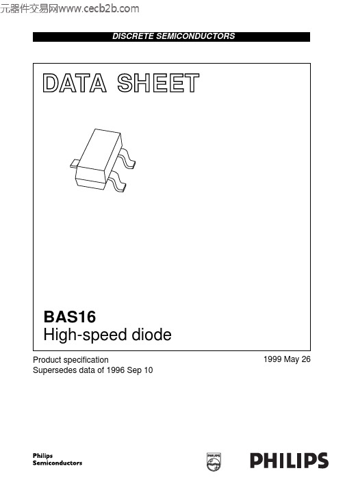
DATASHEETProduct specificationSupersedes data of 1996 Sep 101999May 26DISCRETE SEMICONDUCTORSBAS16High-speed diodebook, halfpageM3D088High-speed diodeBAS16FEATURES•Small plastic SMD package •High switching speed: max.4ns •Continuous reverse voltage:max.75V•Repetitive peak reverse voltage:max.85V•Repetitive peak forward current:max. 500mA.APPLICATIONS•High-speed switching in hybrid thick and thin-film circuits.DESCRIPTIONThe BAS16 is a high-speed switchingdiode fabricated in planar technology,and encapsulated in a small SOT23plastic SMD package.PINNINGPIN DESCRIPTION 1anode 2not connected 3cathodeFig.1 Simplified outline (SOT23) and symbol.Marking code: A6p =made in Hong Kong; A6t =made in Malaysia .handbook, halfpage 213MAM1852n.c.13LIMITING VALUESIn accordance with the Absolute Maximum Rating System (IEC 134).Note1.Device mounted on an FR4 printed-circuit board.SYMBOL PARAMETERCONDITIONSMIN.MAX.UNITV RRM repetitive peak reverse voltage −85V V R continuous reverse voltage −75V I F continuous forward current see Fig.2; note 1−215mA I FRM repetitive peak forward current −500mA I FSMnon-repetitive peak forward currentsquare wave; T j =25°C prior to surge; see Fig.4t =1µs −4A t =1ms −1A t =1s−0.5A P tot total power dissipation T amb =25°C; note 1−250mW T stg storage temperature −65+150°C T j junction temperature−150°CHigh-speed diodeBAS16ELECTRICAL CHARACTERISTICS T j =25°C unless otherwise specified.THERMAL CHARACTERISTICS Note1.Device mounted on an FR4 printed-circuit board.SYMBOL PARAMETERCONDITIONSMAX.UNIT V Fforward voltagesee Fig.3I F =1mA 715mV I F =10mA 855mV I F =50mA 1V I F =150mA1.25V I Rreverse currentsee Fig.5V R =25V 30nA V R =75V1µA V R =25V; T j =150°C 30µA V R =75V; T j =150°C50µA C d diode capacitance f =1MHz; V R =0; see Fig.61.5pF t rrreverse recovery timewhen switched from I F =10mA to I R =10mA; R L =100Ω; measured at I R =1mA; see Fig.74nsV frforward recovery voltage when switched from I F =10mA; t r =20ns;see Fig.81.75VSYMBOL PARAMETERCONDITIONSVALUE UNIT R th j-tp thermal resistance from junction to tie-point 330K/W R th j-a thermal resistance from junction to ambientnote 1500K/WHigh-speed diodeBAS16GRAPHICAL DATADevice mounted on an FR4 printed-circuit board.Fig.2Maximum permissible continuous forward current as a function of ambient temperature.0501002002500200MSA562 -115015010050I F (mA)T amb (o C)(1)T j =150°C; typical values.(2)T j =25°C; typical values.(3)T j =25°C; maximum values.Fig.3Forward current as a function of forward voltage.handbook, halfpage02300I F(mA)100200MBG3821V F (V)(1)(3)(2)Fig.4 Maximum permissible non-repetitive peak forward current as a function of pulse duration.Based on square wave currents.T j =25°C prior to surge.handbook, full pagewidthMBG70410t p (µs)1I FSM (A)10210−1104102103101High-speed diode BAS16Fig.5Reverse current as a function of junction temperature.10510410200MGA884100T ( C)jo I R (nA)10310275 V25 VtypmaxV = 75 V RtypFig.6Diode capacitance as a function of reverse voltage; typical values.f =1MHz; T j =25°C.handbook, halfpage08161240.80.60.40.2MBG446V R (V)C d (pF)High-speed diode BAS16Fig.7 Reverse recovery voltage test circuit and waveforms.(1)I R =1mA.handbook, full pagewidtht rr(1)I F toutput signalt rtt p10%90%V Rinput signal V = V I x R R F SR = 50SΩI FD.U.T.R = 50iΩSAMPLING OSCILLOSCOPEMGA881Fig.8 Forward recovery voltage test circuit and waveforms.t rtt p10%90%Iinputsignal R = 50SΩIR = 50iΩOSCILLOSCOPEΩ1 k Ω450 D.U.T.MGA882V frtoutput signalVHigh-speed diodeBAS16PACKAGE OUTLINEUNIT A 1max.b p c D E e 1H E L p Q w v REFERENCESOUTLINE VERSION EUROPEAN PROJECTIONISSUE DATE 97-02-28IECJEDECEIAJmm0.10.480.380.150.093.02.81.41.20.95e 1.92.52.10.550.450.10.2DIMENSIONS (mm are the original dimensions)0.450.15SOT23b pD e 1eAA 1L pQdetail XH EE w M v M ABAB 01 2 mmscaleA 1.10.9cX123Plastic surface mounted package; 3 leadsSOT23High-speed diode BAS16DEFINITIONSData Sheet StatusObjective specification This data sheet contains target or goal specifications for product development. Preliminary specification This data sheet contains preliminary data; supplementary data may be published later. Product specification This data sheet contains final product specifications.Limiting valuesLimiting values given are in accordance with the Absolute Maximum Rating System (IEC 134). Stress above one or more of the limiting values may cause permanent damage to the device. These are stress ratings only and operation of the device at these or at any other conditions above those given in the Characteristics sections of the specification is not implied. Exposure to limiting values for extended periods may affect device reliability.Application informationWhere application information is given, it is advisory and does not form part of the specification.LIFE SUPPORT APPLICATIONSThese products are not designed for use in life support appliances, devices, or systems where malfunction of these products can reasonably be expected to result in personal injury. Philips customers using or selling these products for use in such applications do so at their own risk and agree to fully indemnify Philips for any damages resulting from such improper use or sale.High-speed diode BAS16NOTESHigh-speed diode BAS16NOTESPhilips Semiconductors Product specification High-speed diode BAS16NOTES1999May2611© Philips Electronics N.V. SCA All rights are reserved. Reproduction in whole or in part is prohibited without the prior written consent of the copyright owner.The information presented in this document does not form part of any quotation or contract, is believed to be accurate and reliable and may be changed without notice. No liability will be accepted by the publisher for any consequence of its use. Publication thereof does not convey nor imply any license under patent- or other industrial or intellectual property rights.Internet: 199965Philips Semiconductors – a worldwide company Netherlands: Postbus 90050, 5600PB EINDHOVEN, Bldg.VB,Tel.+31402782785,Fax.+31402788399New Zealand: 2Wagener Place, C.P.O.Box 1041, AUCKLAND,Tel.+6498494160,Fax.+6498497811Norway: Box 1, Manglerud 0612, OSLO,Tel.+4722748000,Fax.+4722748341Pakistan: see Singapore Philippines: Philips Semiconductors Philippines Inc.,106Valero St.Salcedo Village, P.O.Box 2108MCC,MAKATI,Metro MANILA, Tel.+6328166380,Fax.+6328173474Poland: Ul.Lukiska 10, PL 04-123WARSZAWA,Tel.+48226122831,Fax.+48226122327Portugal: see Spain Romania: see Italy Russia: Philips Russia, atcheva 35A, 119048MOSCOW,Tel.+70957556918,Fax.+70957556919Singapore: Lorong 1, Toa Payoh, SINGAPORE 319762,Tel.+653502538,Fax.+652516500Slovakia: see Austria Slovenia: see Italy South Africa: S.A. PHILIPS Pty Ltd., 195-215Main Road Martindale,2092JOHANNESBURG, P.O.Box 58088 Newville 2114,Tel.+27114715401,Fax.+27114715398South America: Al.Vicente Pinzon,173, 6th floor,04547-130SÃO PAULO,SP, Brazil,Tel.+55118212333,Fax.+55118212382Spain: Balmes 22, 08007BARCELONA,Tel.+34933016312,Fax.+34933014107Sweden: Kottbygatan 7, Akalla, S-16485STOCKHOLM,Tel.+46859852000,Fax.+46859852745Switzerland: Allmendstrasse 140, CH-8027ZÜRICH,Tel.+4114882741Fax.+4114883263Taiwan: Philips Semiconductors, 6F, No.96, Chien Kuo N.Rd.,Sec.1,TAIPEI, Taiwan Tel.+886221342886,Fax.+886221342874Thailand: PHILIPS ELECTRONICS (THAILAND) Ltd.,209/2Sanpavuth-Bangna Road Prakanong, BANGKOK 10260,Tel.+6627454090,Fax.+6623980793Turkey: Yukari Dudullu, Org. San. Blg., 2.Cad. Nr. 28 81260Umraniye,ISTANBUL, Tel.+902165221500,Fax.+902165221813Ukraine : PHILIPS UKRAINE, 4Patrice Lumumba str., Building B, Floor 7,252042KIEV, Tel.+380442642776, Fax. +380442680461United Kingdom: Philips Semiconductors Ltd., 276Bath Road, Hayes,MIDDLESEX UB35BX, Tel.+441817305000,Fax.+441817548421United States: 811East Arques Avenue, SUNNYVALE, CA 94088-3409,Tel.+18002347381, Fax.+18009430087Uruguay: see South America Vietnam: see Singapore Yugoslavia: PHILIPS, Trg N. Pasica 5/v, 11000BEOGRAD,Tel.+38111625344,Fax.+38111635777For all other countries apply to: Philips Semiconductors,International Marketing &Sales Communications, Building BE-p, P.O.Box 218,5600MD EINDHOVEN, The Netherlands,Fax.+31402724825Argentina: see South AmericaAustralia: 34 Waterloo Road, NORTH RYDE, NSW 2113,Tel.+61298054455,Fax.+61298054466Austria:Computerstr. 6, A-1101 WIEN, P.O. Box 213,Tel.+431601011248, Fax.+431601011210Belarus: Hotel Minsk Business Center, Bld.3, r.1211, Volodarski Str.6,220050MINSK, Tel.+375172200733,Fax.+375172200773Belgium: see The NetherlandsBrazil:see South AmericaBulgaria:Philips Bulgaria Ltd., Energoproject, 15th floor,51James Bourchier Blvd., 1407SOFIA,Tel.+3592689211,Fax.+3592689102Canada: PHILIPS SEMICONDUCTORS/COMPONENTS,Tel.+18002347381, Fax.+18009430087China/Hong Kong: 501Hong Kong Industrial Technology Centre,72Tat Chee Avenue, Kowloon Tong, HONG KONG,Tel.+852********,Fax.+852********Colombia: see South AmericaCzech Republic: see AustriaDenmark: Sydhavnsgade 23, 1780COPENHAGEN V,Tel.+4533293333,Fax.+4533293905Finland: Sinikalliontie 3, FIN-02630ESPOO,Tel.+3589615800,Fax.+358961580920France: 51Rue Carnot, BP317, 92156SURESNES Cedex,Tel.+33140996161,Fax.+33140996427Germany: Hammerbrookstraße 69, D-20097HAMBURG,Tel.+4940235360,Fax.+494023536300Hungary:see AustriaIndia: Philips INDIA Ltd, Band Box Building, 2nd floor,254-D,Dr.Annie Besant Road, Worli, MUMBAI 400025,Tel.+91224938541,Fax.+91224930966Indonesia: PT Philips Development Corporation, Semiconductors Division,Gedung Philips, Jl. Buncit Raya Kav.99-100, JAKARTA 12510,Tel.+62217940040ext.2501, Fax.+62217940080Ireland: Newstead, Clonskeagh, DUBLIN 14,Tel.+35317640000,Fax.+35317640200Israel: RAPAC Electronics, 7Kehilat Saloniki St, PO Box 18053,TEL AVIV 61180, Tel.+97236450444,Fax.+97236491007Italy: PHILIPS SEMICONDUCTORS, Piazza IV Novembre 3,20124MILANO, Tel.+390267522531,Fax.+390267522557Japan: Philips Bldg 13-37, Kohnan 2-chome, Minato-ku,TOKYO 108-8507, Tel.+81337405130,Fax.+81337405057Korea: Philips House, 260-199Itaewon-dong, Yongsan-ku, SEOUL,Tel.+8227091412,Fax.+8227091415Malaysia: No.76Jalan Universiti, 46200PETALING JAYA, SELANGOR,Tel.+60 37505214,Fax.+6037574880Mexico: 5900Gateway East, Suite 200, EL PASO, TEXAS 79905,Tel.+9-58002347381, Fax +9-58009430087Middle East: see Italy Printed in The Netherlands 115002/03/pp12 Date of release: 1999May 26Document order number: 939775005878。
BOSCH GDS 18 E-使用说明

安全事項
如果在工作中電纜破損或斷開,不要觸摸電纜,並應立即拔掉插頭。不要使用電 纜破損的電批。
佩帶防護手套、耳塞和防護鞋。 在操作過程中,要始終用雙手持著電批,並要保證站穩。 不要用電纜來拖拉電批。 在戶外使用時,只可使用適於室外使用的延長線和插座。 始終將電纜保持在電批的後面。 只有在停機時才可將電批置於螺絲/螺母之上。 只有使用廠家提供的配件,Bosch 才能保證運轉無故障。
保養和清潔
在對電批進行任何保養和清潔時,應拔掉電源。 為安全和恰當使用,始終保持電機和通風槽清潔。 始終保持電批頭安裝處清潔。
緊鎖扭距
螺絲連接的緊鎖扭距大小取決於電批打的時間。在打了 3 至 5 秒後,扭距達到最 大。此後,扭距增加很少,但電機前部卻顯著變熱。 過熱會導致電批機械元件磨損速度,並提高潤滑要求。
操作指引
只有在停機時才可將電批置於螺絲/螺母之上。 始終用一個扭力計測定實際施加的緊鎖扭距。 扭轉棒 不同直徑的扭轉棒均有扭距限制作用。按鈕應該設為最大。電批打的時間應通過 試驗獲得。
消防调试---FC18调试手册V02.0
FS18 火灾报警系统调试维护手册FS18火灾报警系统调试维护手册FD18 现场设备FC18火灾报警控制器(联动型)JB-TGZL-FC18R火灾报警控制器(联动型)版本:V02.0FS18 火灾报警系统调试维护手册西门子西伯乐斯电子有限公司保留此手册最终解释权。
任何单位和个人未经授权不得发布或者传播此手册内容。
本调试维护手册适用于西门子FS18火灾报警系统的调试和维护。
本手册中的常规条款也可在线或致电索取。
西门子西伯乐斯电子有限公司将尽力避免文中的印刷及图片错误,但并不对可能出现的疏忽承担责任。
文中提到的产品参数以及适用说明如有更新,恕不另行通知。
西门子西伯乐斯电子有限公司版权所有,Copyright © 2006-2009FS18 火灾报警系统调试维护手册目录1概述 (1)2安全 (3)2.1安全提示 (3)2.2安全操作规程 (3)3系统设计 (4)3.1FS18系统示意图 (4)3.2探测回路拓扑结构 (5)3.3隔离模块应用规则 (6)3.4负载因子计算 (8)3.5传输距离 ····································································································································错误!未定义书签。
BAS20-V-GS18中文资料

BAS19-V / 20-V / 21-VDocument Number 85540Rev. 1.5, 22-Jul-05Vishay Semiconductors1Small Signal Switching Diodes, High VoltageFeatures•Silicon Epitaxial Planar Diode•Fast switching diode in case SOT-23,especially suited for automatic insertion.•These diodes are also available in othercase styles including:the SOD-123 case with the type designations BAV19W-V to BAV21W-V, the Mini-MELF case with the type designationBAV101 to BAV103, the DO-35 case with the type designations BAV19-V to BAV21-V and the SOD-323 case with type designation BAV19WS-V to BAV21WS-V.•Lead (Pb)-free component•Component in accordance to RoHS 2002/95/EC and WEEE 2002/96/ECMechanical DataCase: SOT-23 Plastic case Weight: approx. 8.8 mgPackaging Codes/Options:GS18 / 10 k per 13" reel (8 mm tape), 10 k/box GS08 / 3 k per 7" reel (8 mm tape), 15 k/boxParts TablePartT ype differentiation Ordering codeMarkingRemarks BAS19-V V RRM = 120 V BAS19-V-GS18 or BAS19-V-GS08A8T ape and Reel BAS20-V V RRM = 200 V BAS20-V-GS18 or BAS20-V-GS08A81T ape and Reel BAS21-VV RRM = 250 VBAS21-V-GS18 or BAS21-V-GS08A82T ape and Reel 2Document Number 85540Rev. 1.5, 22-Jul-05BAS19-V / 20-V / 21-VVishay Semiconductors Absolute Maximum RatingsT amb = 25°C, unless otherwise specified1) Measured under pulse conditions; Pulse time = T p ≤ 0.3 ms2)Device on fiberglass substrate, see layout on next pageThermal CharacteristicsT amb = 25°C, unless otherwise specified1) Device on fiberglass substrate, see layout on next pageElectrical CharacteristicsT amb = 25°C, unless otherwise specifiedParameterTest conditionPart Symbol Value Unit Continuous reverse voltageBAS19-V V R 100V BAS20-V V R 150V BAS21-VV R 200V Repetitive peak reverse voltageBAS19-V V RRM 120V BAS20-V V RRM 200V BAS21-VV RRM 250V Non-repetitive peak forward currentt = 1 µs I FSM 2.5A Non-repetitive peak forward surge currentt = 1 sI FSM 0.5A Maximum average forward rectified current (av. over any 20 ms period)I F(AV)2001)mA DC forward currentT amb = 25°CI F 2002)mA Repetitive peak forward current I FRM 625mA Power dissipationT amb = 25°CP tot2502)mWParameterT est condition Symbol Value Unit Thermal resistance junction to ambient air R thJA 4301)°C Junction temperature T j 150°C Storage temperature rangeT S- 65 to + 150°CParameterTest conditionSymbol MinTyp.Max Unit Forward voltage I F = 100 mA V F 1.0V I F = 200 mA V F 1.25V Leakage currentV R = V RmaxI R 100nA V R = V Rmax , T j = 150°C I R 100µA Dynamic forward resistance I F = 10 mA r f 5ΩDiode capacitance V R = 0, f = 1 MHzC tot 5pF Reverse recovery timeI F = I R = 30 mA, R L = 100 Ω, I rr = 3 mAt rr50nsBAS19-V / 20-V / 21-VDocument Number 85540Rev. 1.5, 22-Jul-05Vishay Semiconductors3Test Circuit and WaveformsLayout for R thJA testThickness:Fiberglass 1.5 mm (0.059 in.)Copper leads 0.3 mm (0.012 in.) 4Document Number 85540Rev. 1.5, 22-Jul-05BAS19-V / 20-V / 21-V Vishay SemiconductorsPackage Dimensions in mm (Inches)BAS19-V / 20-V / 21-VDocument Number 85540Rev. 1.5, 22-Jul-05Vishay Semiconductors5Ozone Depleting Substances Policy StatementIt is the policy of Vishay Semiconductor GmbH to1.Meet all present and future national and international statutory requirements.2.Regularly and continuously improve the performance of our products, processes, distribution and operating systems with respect to their impact on the health and safety of our employees and the public, as well as their impact on the environment.It is particular concern to control or eliminate releases of those substances into the atmosphere which are known as ozone depleting substances (ODSs).The Montreal Protocol (1987) and its London Amendments (1990) intend to severely restrict the use of ODSs and forbid their use within the next ten years. Various national and international initiatives are pressing for an earlier ban on these substances.Vishay Semiconductor GmbH has been able to use its policy of continuous improvements to eliminate the use of ODSs listed in the following documents.1.Annex A, B and list of transitional substances of the Montreal Protocol and the London Amendments respectively2.Class I and II ozone depleting substances in the Clean Air Act Amendments of 1990 by the Environmental Protection Agency (EPA) in the USA3.Council Decision 88/540/EEC and 91/690/EEC Annex A, B and C (transitional substances) respectively.Vishay Semiconductor GmbH can certify that our semiconductors are not manufactured with ozone depleting substances and do not contain such substances.We reserve the right to make changes to improve technical designand may do so without further notice.Parameters can vary in different applications. All operating parameters must be validated for each customer application by the customer. Should the buyer use Vishay Semiconductors products for any unintended or unauthorized application, the buyer shall indemnify Vishay Semiconductors against all claims, costs, damages, and expenses, arising out of, directly or indirectly, any claim of personaldamage, injury or death associated with such unintended or unauthorized use.Vishay Semiconductor GmbH, P.O.B. 3535, D-74025 Heilbronn, GermanyDocument Number: 91000Revision: 18-Jul-081DisclaimerLegal Disclaimer NoticeVishayAll product specifications and data are subject to change without notice.Vishay Intertechnology, Inc., its affiliates, agents, and employees, and all persons acting on its or their behalf (collectively, “Vishay”), disclaim any and all liability for any errors, inaccuracies or incompleteness contained herein or in any other disclosure relating to any product.Vishay disclaims any and all liability arising out of the use or application of any product described herein or of any information provided herein to the maximum extent permitted by law. The product specifications do not expand or otherwise modify Vishay’s terms and conditions of purchase, including but not limited to the warranty expressed therein, which apply to these products.No license, express or implied, by estoppel or otherwise, to any intellectual property rights is granted by this document or by any conduct of Vishay.The products shown herein are not designed for use in medical, life-saving, or life-sustaining applications unless otherwise expressly indicated. Customers using or selling Vishay products not expressly indicated for use in such applications do so entirely at their own risk and agree to fully indemnify Vishay for any damages arising or resulting from such use or sale. Please contact authorized Vishay personnel to obtain written terms and conditions regarding products designed for such applications.Product names and markings noted herein may be trademarks of their respective owners.元器件交易网。
德国S+B主令控制器

德国S+B主令控制器S+B主令开关(锦菲特I895O268848)VNSO9611主令手柄Spohn+Burkhardt控制器主令手柄S+B主令开关产品系列共计有4大类9种型号;MON, STO, ST1, CS1, NS3, VCSO,VNSO, NNSO, NS2。
划分主令型号主要依据主令的工作环境,触电电流和使用级别SPOHN+BURKHARDT 主令、spohn+burkhardt、Spohn+Burkhardt控制器 Spohn&Burkhardt 德国(S+B)Spohn+Burkhardt主令控制器(又称主令手柄), 操纵杆开关,控制手柄, 电位计, 脚踏开关,电阻器,启动器, 便携式操作装置等产品,例如型号:主令控制器VNSO 44.14 AK EA Z 40PN 40PN + 2×PQ1010主令控制器VNSO 4.14 AZ 40PN + 1×PQ1010主令控制器 VNSO 3 14 FNE Z 10P主令控制器 SMON 6K VR Z20.20触点组 40PN (适合VNSO系列主令控制器使用,)电位器 PQ1010 10-0-10K手杆 VNSO-A手杆 VNSO-EA防尘胶套 V041N档位片 NS07-4P卡位轮 NS026K12面板 V048K3脚踏开关 FW1-G2VNS04FU18SKER50VNSO 2218AKEARH9P1.9P1VNSO 23FN 14KK VRH20.40VNSO 23FN 11SK VRH20.40VNSO 23FN 18AK VRH20.40VNSO 23FN 14KK HRH20.40 VNSO 23FN 11SK HRH20.40 VNSO 23FN 18AK HRH20.40 VNSO 34.14KK AARTU40.50 VNSO 34.11SK AARTU40.50 VNSO 34.18AK AARTU40.50K VCSO 72 14KK VR H40.9P1K VCSO 96 11SK EB H40.9P1K VCSO S 14AK VR H40.9P1CS1 G 11KK VRZ 1 1 G55CS1 72 14KK EXRLZ 1 1 G55CS1 S 11KK EYRLZ 1 1 G55 UGAL 12HR 2RD 5TDHUGAL 12HR 2RD 5TDPUGA 8HR 2RD 5TDHUGAL 12HL 2RD 5TDHUGA 8HL 2RD 5TDPUGAR 12HR 2RD 5TDH UGARL 8HL 2RD 5TDPSMON6VRHD10.10SMON6VRHD10B55GMON6K VRZ8P1.8P1++ESS104 GMON6K EXRZ8P1.8P1++ESS104 GMON6K EYRZ8P1.8P1++ESS104 SMON6K VRZ8P1.8P1++ESS104 SMON6K EXRZ8P1.8P1++ESS104 SMON6K EYRZ8P1.8P1++ESS104 STO(N)BZ30XSTO(N)RG1PSTO(N)RB1NSUGN81BK2RDTG10UG81BK2RDTG10UGD121BK2RDTG10G1S2KTDTRG1S0KTDTRG2S0KTROGNG2S2KTROGNG13 12T11DTLB1ZAIG13 8T11DTLB1ZAISpohn+burkhardt编码器Spohn+burkhardt编码器OGR8B-1 Spohn+burkhardt编码器OGR8G-2 Spohn+burkhardt编码器OGR020-3 Spohn+burkhardt编码器OGR420-4 Spohn+burkhardt编码器OGR420-S0 主令控制器订货号:L5960107L5960108L5960110L5960111L5960112VNSO系列VNSO-218SKFNRHUK9P1 1*0GR8 VNSO-2218KKEARHUK9P1 2*OGR8GVNSO 33FU 18AK VZVNSO 33FU 14 AK VIPZVNSO 3FN 18SK EZVNS0 3 FN 14 SK EIPZVNS04FU18SKER50VNSO 2218AKEARH9P1.9P1 VNSO 23FN 14KK VRH20.40 VNSO 23FN 11SK VRH20.40 VNSO 23FN 18AK VRH20.40 VNSO 23FN 14KK HRH20.40 VNSO 23FN 11SK HRH20.40 VNSO 23FN 18AK HRH20.40 VNSO 34.14KK AARTU40.50 VNSO 34.11SK AARTU40.50 VNSO 34.18AK AARTU40.50K VCSO 72 14KK VR H40.9P1K VCSO 96 11SK EB H40.9P1K VCSO S 14AK VR H40.9P1CS1 G 11KK VRZ 1 1 G55CS1 72 14KK EXRLZ 1 1 G55CS1 S 11KK EYRLZ 1 1 G55 UGAL 12HR 2RD 5TDHUGAL 12HR 2RD 5TDPUGA 8HR 2RD 5TDHUGAL 12HL 2RD 5TDHUGA 8HL 2RD 5TDPUGAR 12HR 2RD 5TDHSMON6VRHD10.10SMON6VRHD10B55GMON6K VRZ8P1.8P1++ESS104 GMON6K EXRZ8P1.8P1++ESS104 GMON6K EYRZ8P1.8P1++ESS104 SMON6KVRZ8P1.8P1++ESS104SMON6K EXRZ8P1.8P1++ESS104SMON6K EYRZ8P1.8P1++ESS104STO(N)BZ30XSTO(N)RG1PSTO(N)RB1NSUGN81BK2RDTG10UG81BK2RDTG10UGD121BK2RDTG10G1S2KTDTRG1S0KTDTRG2S0KTROGNG2S2KTROGNG13 12T11DTLB1ZAIG13 8T11DTLB1ZAISpohn+burkhardt编码器OGR8B-1OGR8G-2OGR020-3OGR420-4OGR420-S0S+B 万向主令 VNSO 33FU 18AK VZS+B 万向主令 VNSO 33FU 14 AK VIPZS+B 单向主令 VNSO 3 FN 18SK EZS+B VNSO 3FA 14SK ER IZS+B 编码器 TYPE:0GR8G-1 VO1T:9-36VDC ARTS+B VNSO 11 14AK EAR K8P1.1+1XPQS55S+B VNS0 3 FN 14 SK EIPZS+B 主令控制和操作机构 VNSOVIPZS+B 主令控制和操作机构 VNSOEIPZS+B 主令控制器 VNSO 22FN 18KKVRHDSZ10P.10P+2*OER8B S+B 主令控制器 VNSO 2FU18SKERHDSZ10P+1*OER8BS+B 主令控制器 VNSO 33FN 18AK VRIPZS+B VNSO 1FN 18ER SS 7114A3S+B VNSO22FX11KKVR BNSWS+B 主令控制器 CS1 72 14 ER Z 10S+B 主令控制器 CS1 72 14 KK VR Z 10.10S+B 主令控制器VNS022 11AK EAR 10P、10P SS 12473-L+2×OGR8B-1S+B 主钩付钩 XKDF12540000S+B 付钩 XKDF12640000S+B 小车大车 1XKDF12440440S+B 小车大车 2XKDF12340440S+B OGR8G-1S+B 主令控制器 VCSO9611ERT8P1+OGF6BS+B 电位计 PD550-5KO/5K0S+B 触点组 40PNS+B 面板 V048K3S+B 防尘胶套 V041NS+B 主令控制器 VNSO 12 14AK EAR K 8P1.10P+2XPQS55S+B 主令控制器 VNSO 11 14AK EAR K 8P1.10P+1XPQS55选型说明VNSO 23 FN 18 KK VR H 20. 40 +2*OGR8GVNSO 代表产品系列,还可以是VCSO 或MON或NSO系列23 代表主令控制器有两个方向,其中一个方向有2副触点,另一方向有3副触点。
- 1、下载文档前请自行甄别文档内容的完整性,平台不提供额外的编辑、内容补充、找答案等附加服务。
- 2、"仅部分预览"的文档,不可在线预览部分如存在完整性等问题,可反馈申请退款(可完整预览的文档不适用该条件!)。
- 3、如文档侵犯您的权益,请联系客服反馈,我们会尽快为您处理(人工客服工作时间:9:00-18:30)。
BAS16D-VDocument Number 85723Rev. 1.2, 06-Apr-05Vishay Semiconductors117431Small Signal Fast Switching DiodeFeatures•Silicon Epitaxial Planar Diode •Fast switching diode•Also available in case SOT-23 with des-ignation BAS16•Lead (Pb)-free component•Component in accordance to RoHS 2002/95/EC and WEEE 2002/96/ECMechanical DataCase: SOD-123 Plastic case Weight: approx. 9.3 mgPackaging Codes/Options:GS18 / 10 k per 13" reel (8 mm tape), 10 k/box GS08 / 3 k per 7" reel (8 mm tape), 15 k/boxParts TableAbsolute Maximum RatingsT amb = 25°C, unless otherwise specified1)Valid provided electrodes are kept at ambient temperaturePartOrdering codeMarkingRemarksBAS16D-VBAS16D-V-GS18 or BAS16D-V-GS08A6Tape and ReelParameterT est condition Symbol Value Unit Reverse voltage V R 75V Peak reverse voltage V RM 100V Forward current (continuous)I F 250mA Non-repetitive peak forward currentt = 1 µs I FSM 2.0A t = 1 ms I FSM 1.0A t = 1 sI FSM 0.5A Power dissipationP tot3501)mW 2Document Number 85723Rev. 1.2, 06-Apr-05BAS16D-VVishay Semiconductors Thermal CharacteristicsT amb = 25°C, unless otherwise specified1) Valid provided electrodes are kept at ambient temperatureElectrical CharacteristicsT amb = 25°C, unless otherwise specified1)Valid provided electrodes are kept at ambient temperatureTypical Characteristics (Tamb = 25 °C unless otherwise specified)ParameterTest condition Symbol Value Unit Maximum junction temperature T j 150°C Storage temperatureT S- 65 to 1501)°CParameterTest conditionSymbol Min Typ.Max Unit Forward voltageI F = 1 mA V F 715mV I F = 10 mA V F 855mV I F = 50 mAV F 1.00V I F = 150 mAV F 1.25V Leakage currentV R = 25 V , T J = 150°CI R 30µA V R = 75 VI R 1µA V R = 75 V , T J = 150°CI R 50µA Diode capacitance V R = 0; f = 1 MHz C tot 2pF Reverse recovery time I F = 10 mA to I R = 10 mA, I R = 1 mA, R L = 100 Ωt rr 6ns Thermal resistance junction to ambient airR thJA3751)°C/WFigure 1. Forward characteristics Figure 2. Dynamic Forward Resistance vs. Forward Current17438BAS16D-VDocument Number 85723Rev. 1.2, 06-Apr-05Vishay Semiconductors3Figure 3. Admissible Power Dissipation vs. Ambient Temperature Figure4. Relative Capacitance vs. Reverse Voltage18186Figure5. Leakage Current vs. Junction Temperature17441Figure6. Admissible Repetitive Peak Forward Current vs. Pulse Duration18106 4Document Number 85723Rev. 1.2, 06-Apr-05BAS16D-VVishay SemiconductorsPackage Dimensions in mm (Inches)BAS16D-VDocument Number 85723Rev. 1.2, 06-Apr-05Vishay Semiconductors5Ozone Depleting Substances Policy StatementIt is the policy of Vishay Semiconductor GmbH to1.Meet all present and future national and international statutory requirements.2.Regularly and continuously improve the performance of our products, processes, distribution and operating systems with respect to their impact on the health and safety of our employees and the public, as well as their impact on the environment.It is particular concern to control or eliminate releases of those substances into the atmosphere which are known as ozone depleting substances (ODSs).The Montreal Protocol (1987) and its London Amendments (1990) intend to severely restrict the use of ODSs and forbid their use within the next ten years. Various national and international initiatives are pressing for an earlier ban on these substances.Vishay Semiconductor GmbH has been able to use its policy of continuous improvements to eliminate the use of ODSs listed in the following documents.1.Annex A, B and list of transitional substances of the Montreal Protocol and the London Amendments respectively2.Class I and II ozone depleting substances in the Clean Air Act Amendments of 1990 by the Environmental Protection Agency (EPA) in the USA3.Council Decision 88/540/EEC and 91/690/EEC Annex A, B and C (transitional substances) respectively.Vishay Semiconductor GmbH can certify that our semiconductors are not manufactured with ozone depleting substances and do not contain such substances.We reserve the right to make changes to improve technical designand may do so without further notice.Parameters can vary in different applications. All operating parameters must be validated for each customer application by the customer. Should the buyer use Vishay Semiconductors products for any unintended or unauthorized application, the buyer shall indemnify Vishay Semiconductors against all claims, costs, damages, and expenses, arising out of, directly or indirectly, any claim of personaldamage, injury or death associated with such unintended or unauthorized use.Vishay Semiconductor GmbH, P.O.B. 3535, D-74025 Heilbronn, GermanyDocument Number: 91000Revision: 18-Jul-081DisclaimerLegal Disclaimer NoticeVishayAll product specifications and data are subject to change without notice.Vishay Intertechnology, Inc., its affiliates, agents, and employees, and all persons acting on its or their behalf (collectively, “Vishay”), disclaim any and all liability for any errors, inaccuracies or incompleteness contained herein or in any other disclosure relating to any product.Vishay disclaims any and all liability arising out of the use or application of any product described herein or of any information provided herein to the maximum extent permitted by law. The product specifications do not expand or otherwise modify Vishay’s terms and conditions of purchase, including but not limited to the warranty expressed therein, which apply to these products.No license, express or implied, by estoppel or otherwise, to any intellectual property rights is granted by this document or by any conduct of Vishay.The products shown herein are not designed for use in medical, life-saving, or life-sustaining applications unless otherwise expressly indicated. Customers using or selling Vishay products not expressly indicated for use in such applications do so entirely at their own risk and agree to fully indemnify Vishay for any damages arising or resulting from such use or sale. Please contact authorized Vishay personnel to obtain written terms and conditions regarding products designed for such applications.Product names and markings noted herein may be trademarks of their respective owners.元器件交易网。