TEMD5510FX01中文资料
TLC5510技术文档
8位高速A/D转换器TLC5510中文资料TLC5510是美国德州仪器(TI)公司生产的8位半闪速结构模数转换器,它采用CMOS工艺制造,可提供最小20Msps的采样率。
可广泛用于数字TV。
医学图像。
视频会议。
高速数据转换以及QAM解调器等方面。
文中介绍了TLC5510的性能指标。
引脚功能。
内部结构和操作时序,给出了TLC5510的应用线路设计和参考电压的配置方法。
1概述TLC5510是美国TI公司生产的新型模数转换器件(ADC),它是一种采用CMOS工艺制造的8位高阻抗并行A/D芯片,能提供的最小采样率为20MSPS。
由于TLC5510采用了半闪速结构及CMOS工艺,因而大大减少了器件中比较器的数量,而且在高速转换的同时能够保持较低的功耗。
在推荐工作条件下,TLC5510的功耗仅为130mW。
由于TLC5510不仅具有高速的A/D转换功能,而且还带有内部采样保持电路,从而大大简化了外围电路的设计;同时,由于其内部带有了标准分压电阻,因而可以从+5V的电源获得2V满刻度的基准电压。
TLC5510可应用于数字TV。
医学图像。
视频会议。
高速数据转换以及QAM解调器等方面。
2内部结构。
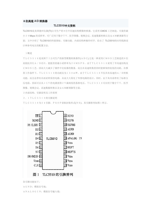
引脚说明及工作原理2.1TLC5510的引脚说明TLC5510为24引脚。
PSOP表贴封装形式(NS)。
其引脚排列如图1所示。
各引脚功能如下:AGND:模拟信号地;ANALOGIN:模拟信号输入端;CLK:时钟输入端;DGND:数字信号地;D1~D8:数据输出端口。
D1为数据最低位,D8为最高位;OE:输出使能端。
当OE为低时,D1~D8数据有效,当OE为高时,D1~D8为高阻抗;VDDA:模拟电路工作电源;VDDD:数字电路工作电源;REFTS:内部参考电压引出端之一,当使用内部电压分压器产生额定的2V基准电压时,此端短路至REFT端;REFT:参考电压引出端之二;REFB:参考电压引出端之三;REFBS:内部参考电压引出端之四,当使用内部电压基准器产生额定的2V基准电压时,此端短路至REFB端。
富士通 生活本LIFEBOOK E5510数据表说明书

Data SheetFujitsu LIFEBOOK E5510Your Powerful and Modern Business DeviceThe FUJITSU Notebook LIFEBOOK E5510 is exclusively designed for office workers needing apowerful, fully-equipped notebook. Thanks to the 10th generation Intel® Core™ processor you can work efficiently wherever you are. The advanced security features like PalmSecure™ are protecting your business data against unauthorized access. Modern Standby provides you an instantly ready and always connected notebook.Modern and robust designReliable mobility, ease of use and modern good looks for everyday business demands Slim 23.9 mm entry notebook starting at 2.04 kg with a solid designEnjoy an ergonomic viewing experience with a 15.6-inch anti-glare FHD display Durability is Military Standard MIL-STD-810H tested Reliable and secure performanceProtect your business data from unauthorized access at all times Integrated PalmSecure™ or finger print sensorInfrared Camera: Allows face recognition with Windows Hello Built-in Privacy Camera Shutter: Protecting your privacy SmartCard reader and TPM 2.0Best in class connectivityBe flexible and stay productive anywhere, anytimeFull set of ports with a full-sized HDMI, VGA and LAN connector and USB Type-C Based on the latest QuadCore Intel processor, enabling data to be processed fasterConvenient serviceability and upgradeabilityEasy access to key components reduces upgrade time and costsBattery, memory, internal storage and connectivity components (LTE & WLAN) can be changed with easeShared port replicator conceptProtect your investments and be ready for shared desk conceptsShared family port replicator with the LIFEBOOK U7 family ensures ultimate flexibility andworkplace sharingComponentsBase unit LIFEBOOK E5510Operating systemsOperating system pre-installed Windows 10 Pro. Fujitsu recommends Windows 11 Pro for business.Windows 10 HomeOperating system compatible Windows 11 Pro. Fujitsu recommends Windows 11 Pro for business.Windows 11 HomeOperating system notes Windows 10 Support: After the end of the product life Fujitsu will continue to test and support all upcoming Window10 releases for a period of maximum 5 years – depending on the available extension of hardware services throughFujitsu Warranty top ups. For details please see “Fujitsu Service Statement for Windows 10 Semi-Annual-ChannelSupport” at .*Processor only for retail, SMB, education and governmentHard disk notes Accessible capacity may vary, also depending on used software.MultimediaBase unitBase unit LIFEBOOK E5510General system informationChipset IntegratedSupported capacity RAM (min.) 4 GBSupported capacity RAM (max.)64 GBMemory slots 2 SO DIMM (DDR4, 2666 MHz)Memory notes Dual channel supportLAN10/100/1,000 MBit/s Intel® I219LMIntegrated WLAN Intel WiFi 6 AX201BIOS version UEFI Specification 2.7BIOS features InsydeH2O BIOSAudio type On boardAudio codec Realtek ALC255 with MaxxAudioAudio features2x built-in speakers (stereo)MIL-STD tested Yes, selected MIL-STD-810H tests passed.MIL-STD-810H test results are not a guarantee of future performance under identified test conditions.Accidental damage is not covered under standard international limited warranty.DisplayBrightness - typical FHD 250 cd/m²Contrast - typical FHD - 700:1Display notes FHD - Viewing angle: Left/Right 80°, Top 80°, Bottom 80°; Color Gamut: 45%, response time 25 msBase unit LIFEBOOK E5510TFT resolution (DisplayPort)up to 4,096 x 2,160TFT resolution (HDMI)up to 4,096 x 2,160TFT resolution (VGA)up to 1,920 x 1,200Graphics brand name Intel® UHD GraphicsGraphics features 3 Display SupportDirectX® 12OpenGL® 4.5Graphics notes Shared memory depending on main memory size and operating systemInterfacesDC-in1Audio: line-out / headphone 1 (combo port with Audio line-in)Audio: line-in / microphone 1 (combo port with Audio line-out)Internal microphones2x digital array microphones (optional)USB 3.2 Gen1 (5 Gbps) total2x Type-A (1 with Anytime USB charge functionality)USB 3.2 Gen2 (10 Gbps) total1x Type-C (Display-Port Tunnel & Power Delivery)VGA1DisplayPort 1 v1.2 (cannot be used together with HDMI)HDMI 1 v1.4b (cannot be used together with DisplayPort)Ethernet (RJ-45) 1 (with status LED)Memory card slots 1 SD 3.0 StandardSD/microSD card: 2GBSDHC/microSDHC card: 32GBSDXC/microSDXC card: 2TBSpeed Class: up to UHS-I (104MB/s)SmartCard slot 1 (optional)SIM card slot 1 (Micro-SIM, only for models with integrated 4G/LTE module)Docking connector for Port Replicator1Kensington Lock support1Keyboard and pointing devicesKeyboard w/o touchstick (spill-resistant), Keyboard w/ touchstick, Backlit keyboard w/o touchstickNumber of keyboard keys: 106, Keyboard pitch: 18.4 mm, Keyboard stroke: 1.7 mmMulti gesture touchpad with two mouse buttonsStatus LEDPower ButtonWireless technologiesAntennas 2 Dual band WLAN antennas, 2 LTE antennas optionalBluetooth v5.0Integrated WLAN Intel WiFi 6 AX201WLAN encryption WPA/WPA2 (Wi-Fi Protected Access)WLAN notes Import and usage according to country-specific regulations.Integrated LTE or UMTS LTE Sierra Wireless EM7455 (cat.6)LTE Sierra Wireless EM7421 (cat.7)GPS Embedded in 4G module if configured with WWANPower supplyNotes65W AC Adapter for usage with system/ 90W AC Adapter for usage with Port Replicator1st battery Lithium polymer battery 4-cell, 50 WhBattery features Quick Charge: 80% in 1hRuntime 1st battery up to 9 h 50 minBattery notes Battery runtime information is based on worldwide acknowledged BAPCo® MobileMark® 2018. Refer to www.bapco.com for additional details.The BAPCo® MobileMark® Benchmark provides results that enable direct product comparisons betweenmanufacturers. It does not guarantee any specific battery runtime which actually can be lower and may varydepending on product model, configuration, application and power management settings. The battery capacitydecreases slightly with every re-charge and over its lifetime.Dimensions / Weight / EnvironmentalDimensions (W x D x H)379 x 256 x 23.9 mm14.92 x 10.08 x 0.94 inchWeight from 2.04 kgWeight (lbs)from 4.49 lbsWeight notes Weight may vary depending on actual configurationOperating ambient temperature 5 - 35 °C (41 - 95 °F)Dimensions / Weight / EnvironmentalOperating relative humidity20 - 80 %ComplianceProduct LIFEBOOK E5510Model5E15A1Germany GS (Full HD Display only)Europe CECBUSA/Canada FCC (depending on configuration) (planned)Global RoHS (Restriction of hazardous substances)WEEE (Waste electrical and electronic equipment)Microsoft Operating Systems (HCT / HCL entry / WHQL)EPEAT® Silver (dedicated regions), depending on configurationTCO Certified 8.0 (depending on configuration)ENERGY STAR® 8.0MIL-STD-810H testedIndia BISRussia EACChina CCC (depending on configuration)Compliance link https:///sites/certificatesAdditional SoftwareAdditional software (preinstalled)McAfee® LiveSafe™ (provides award-winning antivirus protection for your PC and much more. 30 days trial pre-installed)Waves MaxxAudio (audio enhancer)Fujitsu Plugfree Network (network management utility)Fujitsu Anytime USB Charge UtilityFujitsu Battery UtilityFujitsu Function ManagerFujitsu DeskUpdate (driver and utility tool)Additional software (optional)Recovery DVD for Windows®Drivers & Utilities DVD (DUDVD)CyberLink YouCam (webcam software)Microsoft® Office Professional 2019Microsoft® Office Home and Business 2019(A Microsoft Account is required to activate each copy of these products. For purchase and activation only in theregion in which it was acquired.)ManageabilitySecuritySystem and BIOS Security EraseDiskTrusted Platform Module (TPM 2.0)User Security Embedded PalmSecure™ sensor (optional)Embedded fingerprint sensor (optional)Access protection via internal SmartCard reader (optional)Hard disk passwordUser and supervisor BIOS passwordWarrantyWarranty period 1 year (for countries in EMEIA)Warranty type Bring-in Service / Collect & Return Service (depending on country)Product Support - the perfect extensionRecommended Service9x5, Onsite Response Time: Next Business DaySpare Parts availability at least 5 years after shipment, for details see https:///Recommended AccessoriesPort Replicator for LIFEBOOK U7 and E5 family with key lock(2020)Flexibility, expandability, desktop replacement, investment protection – to name just a few benefits of Fujitsu’s docking options.Order Code: S26391-F1607-L219USB Type-C Port Replicator 2Connect to your peripherals. Adapt to the task on demand. The universal USB Type-C interface supports you to get your peripheral devicesconnected easily. Multiply your USB ports to connect your peripherals as well as your external display via HDMI, DisplayPort or VGA.You also can charge your external USB devices without the need of any additional charger.Order Code:S26391-F3327-L100USB Port Replicator PR09The Fujitsu USB Port Replicator PR09 is the perfect solution for shareddesk environments within a hyperconnected world. It connects yourmobile system to your main peripherals with a single USB plug. This Port Replicator is equipped with the most powerful DisplayLink chipset supporting high performance video streaming with Dualhead-DisplayPort.Highest data throughput is guaranteed due to an USB Type-C based Gen2 Hub-Controller enabling up to 10 Gbit/s data streaming. The newestversion of USB Power Delivery chipset (PD3.0) provides powerful charging during your workday.Order Code: S26391-F6007-L500Battery 4 cell 50 WhThe 4 cell 50 Wh battery requires a voltage of 14.4 V and has a capacity of 3490 mAh. The weight of the battery is 300 gms and the recharge time of the cell is 60 minutes for a 80% charge and 150 minutes for a complete 100% charge.Order Code:S26391-F1616-L100USB-C Hub 4 PortsFujitsu offers the first most powerful USB-C hybrid usage hub, following industrial requirements as well as being ready for office desktop usage. The USB-C Hub 4 Ports from Fujitsu makes connecting all of your USB peripherals a quick and simple process. SuperSpeed USB Type-C makes data transfer to and from external storage faster than ever. The hub dynamically selects the optimal speed for each device, giving you more bandwidth where you need it automatically.Order Code:S26391-F6099-L404Privacy FiltersTo use privacy filters is a must in times of increased safety requirements. Fujitsu’s Privacy Filters block unauthorized views on your screen while you are sitting in an external meeting or working in a train. The front view remains clear for the user’s eyes only. The filters are easy to attach and what’s more: They also protect your screen from small scratches and damages.Order Code:S26391-F6098-L215Prestige Top Case 15 (2021)The Prestige Top Case 15 protects notebooks with up to 15.6-inch screens. A padded top-loading notebook compartment made of shock-absorbing foam ensures additional protection. It’s front pouch is ideal for storing of power adaptors, office supplies or personal items. It is the perfect business case in a practical design.Order Code:S26391-F1120-L50Prestige Case 15 (2021)The Prestige Case 15 protects notebooks with up to 15.6-inch screens. The front compartment provides space for your power cord and office supplies.The large compartment is devided for your notebook and a tablet.Order Code:S26391-F1120-L60ContactAddress: x-xx-x, street, city, state, ZIP code, country Phone: xx-xxxx-xxxx Fax : xx-xxxx-xxxxEmail:********************.com Website: /[country]2023-05-02 CE-ENdelivery subject to availability. Any liability that the data and illustrations are complete, actual or correct is excluded. Designations may be trademarks and/or copyrights of the respective manufacturer, the use of which by third parties for their own purposes may infringe the rights of such ownerMore informationAll rights reserved, including intellectual property rights. Changes to technical data reserved. Delivery subject to availability. Any liability that the data and illustrations are complete, actual or correct is excluded.Designations may be trademarks and/or copyrights of the respective manufacturer, the use of which by third parties for their own purposes may infringe the rights of such owner.For further information see /terms_of_use.html Copyright © Fujitsu Technology Solutions。
TEM600系列模块硬件技术规格书_中性_V1.0
TEM600系列模块硬件技术规格书版本:V1.0修订记录文档版本修改说明发布日期作者V1.0 正式发布目录1前言 (3)1.1概述 (3)1.2缩略语 (3)2产品总体介绍 (5)2.1产品简介 (5)2.2产品定义 (5)2.3模块外形 (5)2.4模块主要功能 (6)3技术规格 (7)3.1总体技术指标 (7)3.2射频接收指标 (7)3.3射频发射指标 (8)3.4电源直流特性 (9)4接口定义 (10)5主要功能接口描述 (12)5.1UART接口(可选功能) (12)5.2USB接口 (13)5.3PCM接口(可选功能) (14)5.4AUDIO接口 (14)5.5RUIM卡接口 (16)5.6控制和通用I/O接口(可选功能) (16)5.7电源接口 (17)5.8天线插座接口 (18)6结构 (19)6.1结构尺寸 (19)6.2M INI PCI E XPRESS连接器 (19)6.3RF连接器 (20)1前言1.1概述本文档介绍了TEM600系列模块的功能、接口、技术规格、外观和结构等相关内容,可以帮助使用本模块的研发工程师提供设计参考。
1.2缩略语表1-1 缩略语ADC Analog-Digital Converter 模数转换AFC Automatic Frequency Control 自动频率控制AGC Automatic Gain Control 自动增益控制ARFCN Absolute Radio Frequency Channel绝对射频信道号NumberB2B Board to Board Connector 板对板连接器BER Bit Error Rate 比特误码率CDMA Code Division Multiple Access 码分多址DAI Digital Audio interface 数字音频接口DAC Digital-to-Analog Converter 数模转换DSP Digital Signal Processor 数字信号处理DTR Data Terminal Ready 数据终端准备好EFR Enhanced Full Rate 增强型全速率EMC Electromagnetic Compatibility 电磁兼容EMI Electro Magnetic Interference 电磁干扰ESD Electronic Static Discharge 静电放电EVDO Evolution Data Only 演进数据优化或者进化的数据FR Full Rate 全速率GPRS General Packet Radio Service 通用分组无线业务HR Half Rate 半速率国际移动设备标识IMEI International Mobile EquipmentIdentityISO International Standards国际标准化组织OrganizationPLL Phase Locked Loop 锁相环PPP Point-to-point protocol 点到点协议RAM Random Access Memory 随机访问存储器ROM Read-only Memory 只读存储器RTC Real Time Clock 实时时钟SMS Short Message Service 短消息服务通用异步接收/发送器UART Universal asynchronousreceiver-transmitterUIM User Identifier Management 用户身份管理USB Universal Serial Bus 通用串行总线VSWR Voltage Standing Wave Ratio 电压驻波比2产品总体介绍2.1产品简介TEM600系列模块是PCI Express Mini Card 1.2标准接口的CDMA2000 1X EVDO Rev.A模块,采用高通最新EVDO单芯片平台QSC6085,支持WinCE/Linux等嵌入式操作系统,具有语音、短信、GPS和高速数据业务等功能。
电源管理IC-TM5101

一、功能概述 低启动电流和工作电流 内置前沿消隐(LEB)内置峰值电流补偿和同步斜坡补偿 内置抖频功能可以降低EMI 逐周期限制电流空载或轻载时降频和跳周期工作模式 异常过流保护过压、欠压、开环、过载、过温、输出短路等保护;二、特性描述TM5101是一款高集成度、高性能的PWM 的电流型开关电源控制器。
适用于充电器、电源适配器等各类小功率的开关电源。
采用DIP8和SO-8封装,完善的保护功能,电路结构简单,成本低。
待机功率低,符合“能源之星”等待机功耗标准要求。
三、典型应用四、产品封装形式及引脚功能采用SOP-8和DIP-8封装管脚序号名称功能描述1 FB 电压反馈引脚,通过连接光耦到地来调整占控比。
2、6、7NC空脚。
3 VDD电源供电输入脚 4 GATE驱动输出脚,外接MOSFET 5 CS 电流检测引脚(MOS 源极),外接电阻来检测MOS 电流 8 GND 接地引脚GND CSNC NC VDD FB NC五、内部框图六、极限参数及推荐值注意:极限参数是定义芯片的工作的极限值,超过这些工作条件时将会使电路功能失常,甚至造成损坏,因此,实际的应用中必须低于推荐值。
符号参数推荐值极限值单位V DD供电电压10~23 30 VV FB FB引脚输入电压0~5.5 -0.3~ 7.0 VV CS CS引脚输入电压-0.3 ~ 5.0 VθJC热阻(结点到外壳) 82.5 °C/WT J工作结点温度-40 ~ +150 °CT STG 存储温度范围-40~ +150 °C°C+130-40~T A工作环境温度 -20~+80T L焊接温度(10秒) 260 °C人体模式, JESD22-A114 2.0ESD 抗静电能力kV机器模式, JESD22-A115 0.2七、电气参数(如非特别指明均指V DD =15V ,T A =25℃)符号 参数测试条件最小值 典型值 最大值单位供电部份 V DD-ON 启动电压 13.5 14.5 15.5 VV DD-OFF 关闭电压 8 9 10 V I DD-ST 启动电流 V DD =V DD-ON – 0.5V520uAI DD-OP 正常工作电流 2.5 4 mAV DD-OVPV DD 过压保护23 24 VV DD-CLAMP V DD 钳位电压 I DD =5mA 25 27 VV DD-BM V DD 跳周期模式电压10 V 反馈部份 A VPWM 比较器增益1.7 V/V Z FB FB 引脚输入阻抗6.0k ΩV FB-OPEN FB 开路电压 4.4 4.7 5.0 V V FB-PL FB 过载电压阀值 3.7 V T PD 过载延时时间50 ms V FB-BM进入跳周期模式FB 电压1.4V电流检测部份Z CS CS 引脚输入阻抗5.0 k Ω V CSTH-H 电流限流值(最大占空比)1.01.1V V CSTH-L 电流限制值(最小占空比) 0.7 0.8 V T LEB 前沿尖峰消隐时间350nsT PD 延时输出时间60 ns八、功能描述启动电压及电流典型的启动电流为5uA ,可以使用阻值较大而功耗较小的启动电阻,以减小功率损耗。
ICS557-01 Datasheet说明书

PCI-EXPRESS CLOCK SOURCEDescriptionThe ICS557-01 is a clock chip designed for use inPCI-Express Cards as a clock source. It provides a pair of differential outputs at 100 MHz in a small 8-pin SOIC package.Using IDT’s patented Phase-Locked Loop (PLL) techniques, the device takes a 25 MHz crystal input and produces HCSL (Host Clock Signal Level) differential outputs at 100 MHz clock frequency. LVDS signal levels can also be supported via an alternative termination scheme.Features•Supports PCI-Express TM HCSL Outputs0.7 V current mode differential pair •Supports LVDS Output Levels•Packaged in 8-pin SOIC•RoHS 5 (green ) or RoHS 6 (green and lead free) compliant packaging•Operating voltage of 3.3 V•Low power consumption•Input frequency of 25 MHz•Short term jitter 100 ps (peak-to-peak)•Output Enable via pin selection•Industrial temperature range availableBlock DiagramPin Assignment Pin DescriptionsPin NumberPinNamePinTypePin Description1OE Input Output Enable signal(H = outputs are enabled, L = outputs are disabled/tristated).Internal pull-up resistor.2X1Input Crystal or clock input. Connect to a 25 MHz crystal or single ended clock. 3X2XO Crystal Connection. Connect to a parallel mode crystal.Leave floating if clock input.4GND Power Connect to ground.5IREF Output A 475Ω precision resistor connected between this pin and groundestablishes the external reference current.6CLK Output HCSL differential complementary clock output.7CLK Output HCSL differential clock output.8VDD Power Connect to +3.3 V.Applications Information External ComponentsA minimum number of external components are required for proper operation.Decoupling CapacitorsDecoupling capacitors of 0.01 μF should be connected between VDD and the ground plane (pin 4) as close to the VDD pin as possible. Do not share ground vias between components. Route power from power source through the capacitor pad and then into IDT pin.CrystalA 25 MHz fundamental mode parallel resonant crystal with C L = 16 pF should be used. This crystal must have less than 300 ppm of error across temperature in order for theICS557-01 to meet PCI Express specifications.Crystal CapacitorsCrystal capacitors are connected from pins X1 to ground and X2 to ground to optimize the accuracy of the output frequency.C L= Crystal’s load capacitance in pFCrystal Capacitors (pF) = (C L- 8) * 2For example, for a crystal with a 16 pF load cap, each external crystal cap would be 16 pF. (16-8)*2=16.Current Source (Iref) Reference Resistor - R RIf board target trace impedance (Z) is 50Ω, then R R = 475Ω(1%), providing IREF of 2.32 mA. The output current (I OH) is equal to 6*IREF.Output TerminationThe PCI-Express differential clock outputs of the ICS557-01 are open source drivers and require an external series resistor and a resistor to ground. These resistor values and their allowable locations are shown in detail in thePCI-Express Layout Guidelines section.The ICS557-01can also be configured for LVDS compatible voltage levels. See the LVDS Compatible Layout Guidelines sectionGeneral PCB Layout RecommendationsFor optimum device performance and lowest output phase noise, the following guidelines should be observed.1. Each 0.01µF decoupling capacitor should be mounted on the component side of the board as close to the VDD pin as possible.2. No vias should be used between decoupling capacitor and VDD pin.3. The PCB trace to VDD pin should be kept as short as possible, as should the PCB trace to the ground via. Distance of the ferrite bead and bulk decoupling from the device is less critical.4. An optimum layout is one with all components on the same side of the board, minimizing vias through other signal layers (any ferrite beads and bulk decoupling capacitors can be mounted on the back). Other signal traces should be routed away from the ICS557-01.This includes signal traces just underneath the device, or on layers adjacent to the ground plane layer used by the device.PCI-Express Layout GuidelinesFigure 1: PCI-Express Device RoutingTypical PCI-Express (HCSL) WaveformLVDS Compatible Layout GuidelinesFigure: LVDS Device RoutingTypical LVDS WaveformAbsolute Maximum RatingsStresses above the ratings listed below can cause permanent damage to the ICS557-01. These ratings are stress ratings only. Functional operation of the device at these or any other conditions above those indicated in the operational sections of the specifications is not implied. Exposure to absolute maximum rating conditions for extended periods can affect product reliability. Electrical parameters are guaranteed only over the recommended operating temperature range.DC Electrical CharacteristicsUnless stated otherwise, VDD = 3.3 V ±5%, Ambient Temperature -40 to +85°C1 Single edge is monotonic when transitioning through region.2 Inputs with pull-ups/-downs are not included.ItemRatingSupply Voltage, VDD, VDDA 5.5 VAll Inputs and Outputs-0.5 V to VDD+0.5 V Ambient Operating Temperature (commercial)0 to +70°C Ambient Operating Temperature (industrial)-40 to +85°C Storage Temperature -65 to +150°C Junction Temperature 125°C Soldering Temperature 260°CESD Protection (Input)2000 V min. (HBM)ParameterSymbolConditions Min.Typ.Max.UnitsSupply Voltage V 3.135 3.465Input High Voltage 1V IH 2.0VDD +0.3V Input Low Voltage 1V IL VSS-0.30.8V Input Leakage Current 2I IL 0 < Vin < VDD-55μA Operating Supply Current I DD With 50Ω and 2 pF load 55mA I DDOE OE =Low35mA Input Capacitance C IN Input pin capacitance 7pF Output Capacitance C OUT Output pin capacitance 6pF Pin Inductance L PIN 5nH Output Resistance Rout CLK outputs 3.0k ΩPull-up ResistorR PUPOE60k ΩAC Electrical Characteristics - CLK/CLKUnless stated otherwise, VDD=3.3 V ±5%, Ambient Temperature -40 to +85°C1 Test setup is R L =50 ohms with2 pF , R R = 475Ω (1%).2 Measurement taken from a single-ended waveform.3 Measurement taken from a differential waveform.4Measured at the crossing point where instantaneous voltages of both CLKOUT and CLKOUT are equal.5 CLKOUT pins are tri-stated when OE is low asserted. CLKOUT is driven differential when OE is high.Thermal Characteristics (8-pin SOIC)ParameterSymbolConditions Min.Typ.Max.UnitsInput Frequency 25MHz Output Frequency 100MHzOutput High Voltage 1,2V OH 660700850mV Output Low Voltage 1,2V OL-150027mV Crossing Point Voltage 1,2Absolute250350550mV Crossing Point Voltage 1,2,4Variation over all edges140mV Jitter, Cycle-to-Cycle 1,380ps Rise Time 1,2t OR From 0.175 V to 0.525 V 175332700ps Fall Time 1,2t OFFrom 0.525 V to 0.175 V175344700ps Rise/Fall Time Variation 1,2125ps Duty Cycle 1,34555%Output Enable Time 5All outputs 30µs Output Disable Time 5All outputs30µs Stabilization Time t STABLEFrom power-up VDD=3.3 V3.0ms Spread Change Timet SPREAD Settling period after spread change3.0msParameterSymbolConditionsMin.Typ.Max.UnitsThermal Resistance Junction to AmbientθJA Still air150°C/W θJA 1 m/s air flow 140°C/W θJA 3 m/s air flow120°C/W Thermal Resistance Junction to CaseθJC40°C/WMarking Diagram (ICS557M-01LF) Marking Diagram (ICS557MI-01LF)Notes:1. ###### is the lot code.2. YYWW is the last two digits of the year, and the week number that the part was assembled.3. “L ” designates Pb (lead) free packaging.4. “I” denotes industrial temperature.5. Bottom marking: (orgin). Origin = country of origin if not USA.Package Outline and Package Dimensions (8-pin SOIC, 150 Mil. Narrow Body) Package dimensions are kept current with JEDEC Publication No. 95Ordering InformationPart / Order Number Marking Shipping Packaging Package Temperature 557M-01LF See Page 8Tubes8-pin SOIC0 to +70° C557M-01LFT Tape and Reel8-pin SOIC0 to +70° C557MI-01LF Tubes8-pin SOIC-40 to +85° C557MI-01LFT Tape and Reel8-pin SOIC-40 to +85° C"LF" suffix to the part number are the Pb-Free configuration and are RoHS compliant.While the information presented herein has been checked for both accuracy and reliability, Integrated Device Technology (IDT) assumes no responsibility for either its use or for the infringement of any patents or other rights of third parties, which would result from its use. No other circuits, patents, or licenses are implied. This product is intended for use in normal commercial applications. Any other applications such as those requiring extended temperature range, high reliability, or other extraordinary environmental requirements are not recommended without additional processing by IDT. IDT reserves the right to change any circuitry or specifications without notice. IDT does not authorize or warrant any IDT product for use in life support devices or critical medical instruments.Corporate HeadquartersIntegrated Device Technology, For Sales800-345-7015408-284-8200Fax: 408-284-2775For Tech Support/go/clockhelpInnovate with IDT and accelerate your future networks. Contact:www.IDT .com。
Fluke MDA-510和MDA-550电动驱动分析仪数据表说明书

Simplify complex motor-drive troubleshooting with guided test setups and automated drivemeasurements that provide reliable, repeatable test results.The new Fluke MDA 510 and MDA 550 Motor-Drive Analyzers save time and eliminate the hassle of setting up complex measurements, while simplifying the troubleshooting process. Simply select a test and the step-by-step guided measurements show youwhere to make voltage and current connections, while the preset measurement profiles ensure you will capture all the data you need for each critical motor-drive section—from the input to the output, the DC bus, and the motor itself. From basic to advanced measurements, the MDA-500 Series has you covered, and with a built-in report generator you can quickly and easily generate as-found, and as-left reports with confidence.The MDA-510 and MDA-550 are the ideal portable motor-drive analysis test tools, and can help safely locate and troubleshoot typical problems on inverter type motor-drive systems.• • ••••KEY MEASUREMENTSInverter output voltage, DC bus voltage and ripple voltage, harmonics, unbalance THREE POWERFUL TEST TOOLS IN ONEMotor-drive analyzer, waveform analyzer and recording data logger all in oneHIGHEST SAFETY RATING IN THE INDUSTRY600 V CAT IV/1000 V CAT III rated for use at the service entrance and downstreamThe Fluke MDA-510 and MDA-550 Motor Drive Analyzers use guided test measurements to make analysis easier than everDrive inputMeasure input voltage and current to quickly see whether values are within acceptable limits by comparing the drive’s nominal rated voltage to the actual supplied voltage. Then, check the input current to determine if the current is within the maximum rating and the conductors are suitably sized. You can also check whether the harmonic distortion is within an acceptable level by visu-ally inspecting the waveform shape or by viewing the harmonics spectrum screen (MDA-550) which shows both the total harmonic distortion and individual harmonics.Voltage and current unbalanceCheck the voltage unbalance at the input terminals so you canensure the phase unbalance is not too high (> 6-8 %), and that thephase rotation is correct. You can also check the current unbalance, as excessive unbalance may indicate a drive rectifier problem.Extended harmonic measurementsExcessive harmonics are not just a threat to your rotating machines but also to other equipment connected to the electrical powersystem. The MDA-550 provides the ability to discover the harmon-ics of the motor-drive but can also discover the possible effects of inverter switching electronics. The MDA-550 has three harmonic ranges, 1st to 51st Harmonics, 1 to 9 kHz and 9 kHz to 150 kHz giving the ability to detect any harmonic pollution problems.DC busIn a motor-drive the conversion of AC to DC inside the drive is critical, having the correct voltage and adequate smoothing with low ripple is required for the best drive performance. High ripple voltage may be an indicator of failed capacitors or incorrect sizing of the connected motor. The record function of the MDA-500 Series can be used to check DC bus performance dynamically in the oper-ating mode while a load is applied.Drive outputCheck the output of the drive focusing both on voltage to frequency ratio (V/F), and voltage modulation. When high V/F ratio measure-ments are experienced, the motor may overheat. With low V/Fratios, the connected motor may not be able to provide the requiredtorque at the load to sufficiently run the intended process.Drive input step-by-step guided measurement connectionsDrive output waveform with auto triggeringExtended harmonics spectrum from 9 kHz to 150 kHzVoltage modulationMeasurements of the Pulse Width Modulated signal are used to check for high voltage peaks which can damage motor winding insulation. The rise time or steepness of impulses is indicated by the dV/dt reading (rate of voltage change over time), this should be compared to the motor’s specified insulation. The measure-ments can also be used to measure switching frequency to identify whether there is a potential issue with electronic switching, or with grounding, where the signal floats up and down.Motor inputEnsuring that voltage is being supplied at the motor input termi-nals is key, and the selection of cabling from drive to the motoris critical. Incorrect cabling selection can result in both drive and motor damage due to excessive reflected voltage peaks. Checking that the current present at the terminals is within the motor rating is important as over current condition could cause the motor to run hot, decreasing the life of the stator insulation which can result in the early failure of the motor.Motor shaft voltageVoltage pulses from a variable speed drive can couple from a motor’s stator to its rotor, causing a voltage to appear on the rotor shaft. When this rotor shaft voltage exceeds the insulating capac-ity of the bearing grease, flashover currents (sparking) can occur, causing pitting and fluting of the motor bearing race, damage that can cause a motor to fail prematurely. The MDA-550 Series ana-lyzers are supplied with carbon fiber brush probe tips that can easily detect the presence of destructive flashover currents, while the impulse amplitude and count of events will enable you to take action before failure occurs. The addition of this accessory and capability of the MDA-550 allows you to discover potential damage without investing in expensive permanently installed solutions.Step-by-step guided measurements ensure you have the data you need, when you need itThe MDA-500 Series is designed to help you quickly and easily test and troubleshoot typical problems on three-phase and single-phase inverter type motor-drive systems. The on-screen information, and step-by-step setup guidance make it easy to con-figure the analyzer and get the drive measurements you need to make better maintenance decisions, fast. From power input to the installed motor, the MDA-500 provides the measurement capabilityfor the fastest motor-drive troubleshooting.Voltage modulation with zoomMotor shaft voltage discharge event countsQuick and easy measurement setup1) Press ‘Motor Drive Analyzer’ button and select‘Drive Measurement Location’.2) Use the on-screen context information tofurther guide you to successful setup andmeasurement.3) Choose the measurement.4) Select the measurement method/option.5) Connect the test probes according to the dia-gram. Once complete press ‘Next’.6) The analyzer will then automatically trigger,and configure the reading for the optimummeasurements.Reporting and analysisThe MDA-500 Series simplifies the process of gathering data and writing test reports with abuilt-in report generator.At each test point or measurement there is the option to create, update or modify a report. Simply press ‘SAVE TO REPORT’ and select the appropri-ate screens to save into a text based report file. By performing the step-by-step guided measure-ments a comprehensive report can be created directly from the instrument to document the entire troubleshooting process.Input the report name. The single report encom-passes all recorded measurements and can easily be shared with other users and used for motor-drive benchmarking, and for comparing data nowand in the future.Featured measurementsSpecificationsOrdering informationMDA-510Motor drive analyzer, 4 channel, 500 MHzMDA-550Motor drive analyzer, 4 channel, 500 MHz with motor shaft and harmonicsIncludes1x BP 291 li-ion battery pack, 1x BC190 charger/power adapter, 3x VPS 100:1 high voltage probes with alligator clips, 1xVPS410-II-R 10:1 500MHz voltage probe, 1x i400s ac current clamp, 1x C1740 carrying case, 1x 2 GB USB drive with manuals and FlukeView™2 softwareMDA-550 also includes 1x SVS-500 shaft voltage set (3x brush, probe holder, two-piece extension rod and magnetic base), additional 2x i400s ac current clampsAdditional accessoriesSVS-500 set of 3x brushes, probe holder, two-piece extension rod and magnetic baseSB-500 set of 3x replacement brushes*In addition, Fluke 190 series II ScopeMeter™ Test Tools acces-sories are also supported by the MDA-500 Series Fluke CorporationPO Box 9090, Everett, WA 98206 U.S.A.Fluke Europe B.V.PO Box 1186, 5602 BDEindhoven, The NetherlandsFor more information call:In the U.S.A. (800) 443-5853 orFax (425) 446-5116In Europe/M-East/Africa +31 (0) 40 2675 200 or Fax +31 (0) 40 2675 222In Canada (800)-36-FLUKE orFax (905) 890-6866From other countries +1 (425) 446-5500 or Fax +1 (425) 446-5116Web access: ©2018 Fluke Corporation.Specifications subject to change without notice. Printed in U.S.A. 6/2018 6011207b-enModification of this document is not permitted without written permission from Fluke Corporation. Fluke. Keeping your worldup and running.®。
ASUS Infinity (T003) F7905 快速入门指南说明书

F7905Première éditionCopyright © 2013 ASUSTek Computers, Inc.Tous droits réservés.Aucune partie de ce manuel, y compris les produits et logiciels qu’il décrit, ne peut être reproduite, transmise, transcrite, stockée dans un système d’archivage ou traduite en quelque langue, sous quelque forme ou par quelque moyen que ce soit, à l’exception de la documentation conservée par l’acheteur à des fins de sauvegarde, sans l’autorisation expresse écrite d’ASUSTeK COMPUTER INC. (« ASUS »).La garantie du produit ou service ne sera pas prolongée si : (1) le produit est réparé, modifié ou altéré, sauf si cette réparation, modification ou altération est autorisée par écrit par ASUS; ou (2) le numéro de série du produit estdégradé ou manquant.ASUS FOURNIT CE MANUEL « TEL QUEL » SANS GARANTIED’AUCUNE SORTE, EXPRESSE OU IMPLICITE, Y COMPRIS, MAIS SANS S’Y LIMITER, LES GARANTIES OU CONDITIONS DE QUALITÉ MARCHANDE OU D’ADÉQUATION À UN USAGE PARTICULIER. EN AUCUN CAS ASUS, SES ADMINISTRATEURS, DIRIGEANTS, EMPLOYÉS OU AGENTS NE SERONT TENUS RESPONSABLES DE DOMMAGES INDIRECTS, SPÉCIAUX, ACCESSOIRES OU INDIRECTS (Y COMPRIS LES DOMMAGES POUR PERTE DE PROFITS, PERTE D’AFFAIRES, PERTE DE L’UTILISATION OU DE DONNÉES, INTERRUPTION DE COMMERCE ET CAS SIMILAIRES), MÊME SI ASUS A ÉTÉ INFORMÉ DE LA POSSIBILITÉ DE TELS DOMMAGES PROVENANT DE TOUT DÉFAUT OU ERREUR DANS CE MANUEL OU LE PRODUIT.LES SPÉCIFICATIONS ET INFORMATIONS CONTENUES DANS CE MANUEL SONT FOURNIES À TITRE INDICATIF ET PEUVENT CHANGER À TOUT MOMENT SANS PRÉAVIS ET NE DOIVENT PAS ÊTRE INTERPRÉTÉES COMME UN ENGAGEMENT DE LA PART D’ASUS. ASUS N’ASSUME AUCUNE RESPONSABILITÉ POUR TOUTE ERREUR QUI POURRAIT APPARAÎTRE DANS CE MANUEL, Y COMPRIS LES PRODUITS ET LOGICIELS DÉCRITS DANS CELUI-CI.Les produits et noms de sociétés apparaissant dans ce manuel peuvent être ou non des marques commerciales déposées ou des copyrights de leurs sociétés respectives, et sont uniquement utilisés pour identification ou comme explication dans l’intérêt du propriétaire, sans intention de contrefaçon.Merci pour votre achat d’un nouveau produit ASUS !Avant de commencer, assurez-vous de lire toute la documentation importante relative à la sécurité et à l’opération accompagnant ce produit pour éviter de vous blesser ou d’endommager l’appareil.REMARQUE : Ce guide de démarrage rapide est fourni à titre de référence et peut être modifié sans préavis. Pour les dernières mises à jour et pour obtenir des d’informations plus détaillées, veuillez visiter le site .Faire connaissance avec votre PadFone InfinityCaractéristiques de la face avantÉcran tactileÉcouteurCaméra frontale Touches tactilesIMPORTANT ! La première fois que vous allumez votrePadFone Infinity, l’écran de bienvenue apparaît. Sélectionnez votre langue, puis appuyez sur Étape suivante . Suivez les instructions à l’écran pour configurer votre PadFone Infinity.Pour éteindre votre PadFone Infinity :1. Appuyez sur le bouton d’alimentation pendant environ cinq (5) secondes jusqu’à ce que le menu d’extinction apparaisse.2. Appuyez sur Éteindre , puis appuyez sur OK pour confirmer.Allumer ou éteindre le PadFone Infinity Appuyez sur la touche d’alimentation située sur le côte de votre PadFone Infinity pour allumer ou éteindre l’appareil.Bouton Marche/Arrêt。
ST1510FX中文资料
ST1510FX中文资料February 2007Rev 21/10Order codesPart number Marking Package Packing ST1510FX1510FXISOWA TT218FXT ubeST1510FXHigh voltage fast-switchingNPN Power transistorGeneral features■State-of-the-art technology:–Diffused collector “Enhanced generation” EHVS1■More stable performances versus operating temperature variation ■Low base-drive requirements■Tighter h FE range at operating collector current ■Fully insulated power package U.L. compliant ■In compliance with the 2002/93/EC European directiveApplications■Electronic ballast for fluorescent lighting ■Switch mode power suppliesDescriptionThe device is manufactured using DiffusedCollector in Planar technology adopting new and enhanced high voltage structure 1 (E.H.V.S.1).Contents ST1510FXContents1Electrical ratings . . . . . . . . . . . . . . . . . . . . . . . . . . . . . . . . . . . . . . . . . . . . 32 Electrical characteristics . . . . . . . . . . . . . . . . . . . . . . . . . . . . . . . . . . . . . 42.1Electrical characteristics (curve) . . . . . . . . . . . . . . . . . . . . . . . . . . . . . . . . 52.2Testcircuits . . . . . . . . . . . . . . . . . . . . . . . . . . . . . . . . . . . . . . . . . . . . . . . . . 7 3Package mechanical data . . . . . . . . . . . . . . . . . . . . . . . . . . . . . . . . . . . . .8 4Revision history . . . . . . . . . . . . . . . . . . . . . . . . . . . . . . . . . . . . . . . . . . .102/10ST1510FX Electrical ratings3/101 Electrical ratingsTable 2.Thermal dataTable 1.Absolute maximum ratingSymbol ParameterValue Unit V CES Collector-emitter voltage (V BE = 0) 1500V V CEO Collector-emitter voltage (I B = 0) 750V V EBO Collector-base voltage (I C = 0)9V I C Collector current12A I CM Collector peak current (t P < 5ms)20A I B Base current6A P TOT Total dissipation at T c = 25°C62W V isol Insulation withstand voltage (RMS) from all three leads to external heatsink 2500VT stg Storage temperature-65 to 150°CT JMax. operating junction temperature150SymbolParameterValue Unit R thj-case Thermal resistance junction-case _______________max2°C/WElectrical characteristics ST1510FX4/102 Electrical characteristics(T case = 25°C unless otherwise speci fied)Table 3.Electrical characteristicsSymbol ParameterTest conditions Min.Typ.Max.Unit I CES Collector cut-off current (V BE =0)V CE = 1500VV CE = 1500V T C = 125°C 0.22mA mA I EBOEmitter cut-off current (I C =0)V EB = 9V1mAV CEO(sus) (1)Collector-emittersustaining voltage(I B =0)I C = 100mA750VV CE(sat) (1)1.Pulsed: Pulse duration = 300 ms, duty cycle 1.5% Collector-emitter saturation voltage I C = 6A I B = 1.5A 2V V BE(sat) (1)Base-emitter saturation voltageI C = 6A I B = 1.5A 1.1Vh FE (1)DC current gainI C = 1A V CE = 5VI C = 6A V CE = 5V I C = 7A V CE = 1V 156.5285.59.5t s t fInductive load Storage time Fall timeI C = 6A I B(on) = 1.2A I B(off) = -2.4A L = 500μH V clamp = 350V20.2μs μsST1510FX Electrical characteristics5/102.1 Electrical characteristics (curve)Figure 1.Safe operating area Figure 2.Derating curveFigure 3.Output characteristics Figure 4.Reverse biased SOAFigure 5.DC current gain @ V CE =1VFigure 6.DC current gain @ V CE =5VElectrical characteristicsST1510FX6/102.2 Test circuitsFigure 7.Collector emitter saturation Figure 8.Base emitter saturationST1510FX Package mechanical data 3 Package mechanical dataIn order to meet environmental requirements, ST offers these devices in ECOPACK?packages. These packages have a Lead-free second level interconnect. The category ofsecond level interconnect is marked on the package and on the inner box label, incompliance with JEDEC Standard JESD97. The maximum ratings related to solderingconditions are also marked on the inner box label. ECOPACK is an ST trademark.ECOPACK specifications are available at: 7/10Package mechanical data ST1510FX8/10ST1510FX Revision history9/104 Revision historyTable 4.Revision historyDate RevisionChanges02-Nov-20051Initial release.23-Feb-20072Order code and parameters on Table 1 has been changeST1510FX10/10Please Read Carefully:Information in this document is provided solely in connection with ST products. STMicroelectronics NV and its subsidiaries (“ST”) reserve the right to make changes, corrections, modifications or improvements, to this document, and the products and services described herein at any time, without notice.All ST products are sold pursuant to ST’s terms and conditions of sale.Purchasers are solely responsible for the choice, selection and use of the ST products and services described herein, and ST assumes no liability whatsoever relating to the choice, selection or use of the ST products and services described herein.No license, express or implied, by estoppel or otherwise, to any intellectual property rights is granted under this document.If any part of this document refers to any third party products or services it shall not be deemed a license grant by ST for the use of such third party products or services, or any intellectual property contained therein or considered as a warranty covering the use in any manner whatsoever of such third party products or services or any intellectual property contained therein.UNLESS OTHERWISE SET FORTH IN ST’S TERMS AND CONDITIONS OF SALE ST DISCLAIMS ANY EXPRESS OR IMPLIED WARRANTY WITH RESPECT TO THE USE AND/OR SALE OF ST PRODUCTS INCLUDING WITHOUT LIMITATION IMPLIED WARRANTIES OF MERCHANTABILITY, FITNESS FOR A PARTICULAR PURPOSE (AND THEIR EQUIVALENTS UNDER THE LAWS OF ANY JURISDICTION), OR INFRINGEMENT OF ANY PATENT, COPYRIGHT OR OTHER INTELLECTUAL PROPERTY RIGHT. UNLESS EXPRESSLY APPROVED IN WRITING BY AN AUTHORIZED ST REPRESENTATIVE, ST PRODUCTS ARE NOT RECOMMENDED, AUTHORIZED OR WARRANTED FOR USE IN MILITARY, AIR CRAFT, SPACE, LIFE SAVING, OR LIFE SUSTAINING APPLICATIONS, NOR IN PRODUCTS OR SYSTEMS WHERE FAILURE OR MALFUNCTION MAY RESULT IN PERSONAL INJURY, DEATH, OR SEVERE PROPERTY OR ENVIRONMENTAL DAMAGE. ST PRODUCTS WHICH ARE NOT SPECIFIED AS "AUTOMOTIVE GRADE" MAY ONLY BE USED IN AUTOMOTIVE APPLICATIONS AT USER’S OWN RISK.Resale of ST products with provisions different from the statements and/or technical features set forth in this document shall immediately void any warranty granted by ST for the ST product or service described herein and shall not create or extend in any manner whatsoever, any liability of ST.ST and the ST logo are trademarks or registered trademarksof ST in various countries.Information in this document supersedes and replaces all information previously supplied.The ST logo is a registered trademark of STMicroelectronics. All other names are the property of their respective owners.2007 STMicroelectronics - All rights reservedSTMicroelectronics group of companiesAustralia - Belgium - Brazil - Canada - China - Czech Republic - Finland - France - Germany - Hong Kong - India - Israel - Italy - Japan - Malaysia - Malta - Morocco - Singapore - Spain - Sweden - Switzerland - United Kingdom - United States of America 。
- 1、下载文档前请自行甄别文档内容的完整性,平台不提供额外的编辑、内容补充、找答案等附加服务。
- 2、"仅部分预览"的文档,不可在线预览部分如存在完整性等问题,可反馈申请退款(可完整预览的文档不适用该条件!)。
- 3、如文档侵犯您的权益,请联系客服反馈,我们会尽快为您处理(人工客服工作时间:9:00-18:30)。
Document Number: 81293For technical questions, contact: detectortechsupport@Ambient Light Sensor, RoHS Compliant, Released for Lead(Pb)-free Reflow Soldering, AEC-Q101 ReleasedTEMD5510FX01Vishay SemiconductorsDESCRIPTIONTEMD5510FX01 ambient light sensor is a PIN photodiode with high photo sensitivity in a miniature surface mount device (SMD). The detector chip has 7.5 mm 2 sensitive area.It is sensitive to visible light much like the human eye and has peak sensitivity at 540 nm.FEATURES•Package type: surface mount •Package form: top view•Dimensions (L x W x H in mm): 5 x 4.24 x 1.12•Radiant sensitive area (in mm 2): 7.5•Product designed and qualified acc. AEC-Q101for the automotive market •High photo sensitivity•Adapted to human eye responsivity•Supression filter for near infrared radiation •Angle of half sensitivity: ϕ = ± 65°•Floor life: 72 h, MSL 4, acc. J-STD-020•Lead (Pb)-free reflow soldering•Lead (Pb)-free component in accordance with RoHS 2002/95/EC and WEEE 2002/96/ECAPPLICATIONS•Automotive sensors •Ambient light sensors •Backlight dimmers •Notebooks •ComputersNoteTest conditions see table “Basic Characteristics”NoteMOQ: minimum order quantityNoteT amb = 25 °C, unless otherwise specifiedPRODUCT SUMMARYCOMPONENT I ra (µA)ϕ (deg)λ0.5 (nm)TEMD5510FX0126± 65430 to 610ORDERING INFORMATIONORDERING CODE PACKAGING REMARKSPACKAGE FORMTEMD5510FX01Tape and reelMOQ: 1500 pcs, 1500 pcs/reelTop viewABSOLUTE MAXIMUM RATINGSPARAMETER TEST CONDITIONSYMBOLVALUE UNIT Reverse voltage V R 16V Power dissipation T amb ≤ 25 °C P V 215mW Junction temperature T j 100°C Operating temperature range T amb - 40 to + 100°C Storage temperature range T stg - 40 to + 100°C Soldering temperatureAcc. reflow solder profile fig. 5T sd 260°C Thermal resistance junction/ambient Soldered on PCB with pad dimensions: 4 mm x 4 mmR thJA350K/W For technical questions, contact: detectortechsupport@Document Number: 81293TEMD5510FX01Vishay Semiconductors Ambient Light Sensor, RoHS Compliant, Released forLead (Pb)-free Reflow Soldering, AEC-Q101 ReleasedNoteT amb = 25 °C, unless otherwise specifiedBASIC CHARACTERISTICST amb = 25°C, unless otherwise specifiedFig. 1 - Reverse Dark Current vs. Ambient Temperature Fig. 2 - Reverse Light Current vs. Irradiance Fig. 3 - Relative Spectral Sensitivity vs. WavelengthFig. 4 - Relative Radiant Sensitivity vs. Angular DisplacementBASIC CHARACTERISTICSPARAMETER TEST CONDITION SYMBOL MIN.TYP.MAX.UNIT Breakdown voltage I R= 100 µA, E = 0V (BR)16V Reverse dark current V R = 10 V, E = 0I ro 230nA Diode capacitanceV R = 0 V, f = 1 MHz, E = 0C D 1600pF V R = 3 V, f = 1 MHz, E = 0C D 73040pF Reverse light current E e = 1 mW/cm 2, λ = 550 nm,V R = 5 V I ra 26µA E v = 100 lx, CIE illuminant A,V R = 5 VI ra 0.81µA Angle of half sensitivity ϕ± 65deg Wavelength of peak sensitivity λp 540nm Range of spectral bandwidthλ 0.5430 to 610nmTEMD5510FX01 Ambient Light Sensor, RoHS Compliant, Released forVishay Semiconductors Lead (Pb)-free Reflow Soldering, AEC-Q101 ReleasedPACKAGE DIMENSIONSin millimetersDocument Number: 81293For technical questions, contact: detectortechsupport@ For technical questions, contact: detectortechsupport@Document Number: 81293TEMD5510FX01Vishay Semiconductors Ambient Light Sensor, RoHS Compliant, Released forLead (Pb)-free Reflow Soldering, AEC-Q101 ReleasedTAPING DIMENSIONS in millimetersREEL DIMENSIONSin millimetersTEMD5510FX01 Ambient Light Sensor, RoHS Compliant, Released forLead (Pb)-free Reflow Soldering, AEC-Q101 ReleasedVishay Semiconductors SOLDER PROFILEFig. 5 - Lead (Pb)-free Reflow Solder Profileacc. J-STD-020D DRYPACKDevices are packed in moisture barrier bags (MBB) to prevent the products from moisture absorption during transportation and storage. Each bag contains a desiccant. FLOOR LIFETime between soldering and removing from MBB must not exceed the time indicated in J-STD-020:Moisture sensitivity: level 4Floor life: 72 hConditions: T amb < 30 °C, RH < 60 %DRYINGn case of moisture absorption devices should be baked before soldering. Conditions see J-STD-020 or recommended conditions:192 h at 40 °C (+ 5 °C), RH < 5 %or96 h at 60 °C (+ 5 °C), RH < 5 %.Document Number: 81293For technical questions, contact: detectortechsupport@ Disclaimer Legal Disclaimer NoticeVishayAll product specifications and data are subject to change without notice.Vishay Intertechnology, Inc., its affiliates, agents, and employees, and all persons acting on its or their behalf (collectively, “Vishay”), disclaim any and all liability for any errors, inaccuracies or incompleteness contained herein or in any other disclosure relating to any product.Vishay disclaims any and all liability arising out of the use or application of any product described herein or of any information provided herein to the maximum extent permitted by law. The product specifications do not expand or otherwise modify Vishay’s terms and conditions of purchase, including but not limited to the warranty expressed therein, which apply to these products.No license, express or implied, by estoppel or otherwise, to any intellectual property rights is granted by this document or by any conduct of Vishay.The products shown herein are not designed for use in medical, life-saving, or life-sustaining applications unless otherwise expressly indicated. Customers using or selling Vishay products not expressly indicated for use in such applications do so entirely at their own risk and agree to fully indemnify Vishay for any damages arising or resulting from such use or sale. Please contact authorized Vishay personnel to obtain written terms and conditions regarding products designed for such applications.Product names and markings noted herein may be trademarks of their respective owners.元器件交易网Document Number: 。