TSOP39238中文资料
uc3843中文资料 (4)

UC3843中文资料1. 简介UC3843是一款集成了PWM控制电路的高性能电源管理芯片。
它能够通过自身的内部反馈环路来实现稳定的输出电压,并且可调节输出电压范围。
这使得UC3843非常适用于开关电源和DC-DC转换应用中。
UC3843具有低启动电流、内部锁死和内部软启动功能,能够有效地降低功耗和延长系统寿命。
此外,它还具有短路保护、过温保护和欠压保护功能,确保了系统的安全性和可靠性。
2. 特点•集成了PWM控制电路,适用于开关电源和DC-DC转换应用。
•可调节的输出电压范围,能够满足不同应用的需求。
•低启动电流,节省功耗,提高系统效率。
•内部锁死和软启动功能,保护系统并延长使用寿命。
•短路保护、过温保护和欠压保护功能,确保系统安全可靠。
3. 参数规格以下是UC3843的主要参数规格:•输入电压范围:5V至25V•输出电压范围:0V至24V•最大输出电流:1A•工作频率:50kHz至500kHz•工作温度范围:-40°C至125°C•封装:DIP-8、SOP-84. 应用示例UC3843广泛应用于各种开关电源和DC-DC转换器设计中。
以下是一些应用示例:4.1 5V至12V降压转换器UC3843可以用于设计一个从5V输入降压到12V输出的DC-DC转换器。
通过调节内部反馈环路,可以使输出电压保持稳定在12V。
此外,UC3843的低启动电流和软启动功能确保了系统的正常启动和运行。
4.2 24V恒流LED驱动器UC3843还可以用于设计一个24V恒流LED驱动器。
通过控制PWM信号的占空比,可以调节LED的亮度,并通过反馈电路实现恒流驱动。
短路保护和过温保护功能能够保护LED和驱动器的安全性。
4.3 太阳能充电控制器由于UC3843具有广泛的输入电压范围和可调节的输出电压范围,因此非常适合用于设计太阳能充电控制器。
通过控制PWM信号,可以实现对充电电流的精确控制,并通过反馈电路实现恒压和恒流充电。
2N3923中文资料

MIN 50 40 50 80 120 100 100 150 150 45 60 40 50 30 140 140 30 50 80 80 50 55 40 60 60 30 50 30 50 300 300 40 60 40 50 40 30 40 60 150 50 80 100
MIN 150 175 150 200 150 150 150 150 150 200 200 60 60 150 150 200 30 30 60 60 200 250 60 60 300 300 300 300 250 30 30 180 150 180 200 200 500 60 60 40 60 40 40
MAX 12 25 25 7.0 6.0 10 10 8.0 8.0 8.0 8.0 40 40 25 10 10 275 275 12 12 9.0 8.0 120 120 10 12 10 9.0 9.0 6.0 15 15 15 15 12 12 3.0 120 120 3.5 12 60 60
MAX --------------3.0 3.0 ----------------------------
2N3724A NPN CORE DRIVER 2N3725A NPN CORE DRIVER 2N3734 2N3735 2N3742 2N3743 2N3762 2N3763 2N3764 2N3830 2N3831 2N3866 2N3867 2N3868 2N3923 2N3945 2N4000 2N4001 NPN CORE DRIVER NPN CORE DRIVER NPN HIGH VOLTAGE PNP HIGH VOLTAGE PNP CORE DRIVER PNP CORE DRIVER PNP CORE DRIVER NPN CORE DRIVER NPN CORE DRIVER NPN VHF/UHF OSC PNP AMPL/SWITCH PNP AMPL/SWITCH NPN AMPL/SWITCH NPN AMPL/SWITCH NPN AMPL/SWITCH NPN AMPL/SWITCH
TSOP38238中文资料

IR Receiver Modules for Remote Control SystemsTSOP382.., TSOP384.. Vishay SemiconductorsMECHANICAL DATA Pinning:1 = OUT,2 = GND,3 = V S FEATURES•Very low supply current•Photo detector and preamplifier in one package •Internal filter for PCM frequency•Improved shielding against EMI•Supply voltage: 2.5 V to 5.5 V•Improved immunity against ambient light•Insensitive to supply voltage ripple and noise •Component in accordance to RoH S 2002/95/EC and WEEE 2002/96/ECDESCRIPTIONThe TSOP382.., TSOP384.. series are miniaturized receivers for infrared remote control systems. A PIN diode and a preamplifier are assembled on a lead frame, the epoxy package acts as an IR filter.The demodulated output signal can be directly decoded by a microprocessor. The TSOP382.. is compatible with all common IR remote control data formats. The TSOP384.. is optimized to suppress almost all spurious pulses from energy saving fluorescent lamps but will also suppress some data signals.This component has not been qualified according to automotive specifications.BLOCK DIAGRAM APPLICATION CIRCUIT19026PARTS TABLECARRIER FREQUENCY STANDARD APPLICATIONS (AGC2/AGC8)VERY NOISY ENVIRONMENTS (AGC4) 30 kHz TSOP38230TSOP3843033 kHz TSOP38233TSOP3843336 kHz TSOP38236TSOP3843638 kHz TSOP38238TSOP3843840 kHz TSOP38240TSOP3844056 kHz TSOP38256TSOP38456TSOP382.., TSOP384..IR Receiver Modules for Remote Control SystemsVishay SemiconductorsNote(1)Stresses beyond those listed under “Absolute Maximum Ratings” may cause permanent damage to the device. This is a stress rating only and functional operation of the device at these or any other conditions beyond those indicated in the operational sections of this specification is not implied. Exposure to absolute maximum rating condtions for extended periods may affect the device reliability.Note (1)T amb = 25°C, unless otherwise specifiedTYPICAL CHARACTERISTICST amb = 25°C, unless otherwise specifiedFig. 1 - Output Active LowFig. 2 - Pulse Length and Sensitivity in Dark AmbientABSOLUTE MAXIMUM RATINGS (1)PARAMETER TEST CONDITIONSYMBOLVALUE UNIT Supply voltage (pin 3)V S - 0.3 to + 6.0V Supply current (pin 3)I S 3mA Output voltage (pin 1)V O - 0.3 to (V S + 0.3)V Output current (pin 1)I O 5mA Junction temperatureT j 100°C Storage temperature range T stg - 25 to + 85°C Operating temperature range T amb - 25 to + 85°C Power consumption T amb ≤ 85°C P tot 10mW Soldering temperaturet ≤ 10 s, 1 mm from case T sd260°CELECTRICAL AND OPTICAL CHARACTERISTICS (1)PARAMETER TEST CONDITION SYMBOL MIN.TYP.MAX.UNIT Supply current (pin 3)E v = 0, V S = 3.3 V I SD 0.270.350.45mA E v = 40 klx, sunlightI SH 0.45mA Supply voltage V S 2.55.5V Transmission distance E v = 0, test signal see fig. 1,IR diode TSAL6200,I F = 250 mA d 45m Output voltage low (pin 1)I OSL = 0.5 mA, E e = 0.7 mW/m 2,test signal see fig. 1V OSL 100mV Minimum irradiance Pulse width tolerance:t pi - 5/f o < t po < t pi + 6/f o ,test signal see fig. 1E e min.0.150.35mW/m 2Maximum irradiance t pi - 5/f o < t po < t pi + 6/f o ,test signal see fig. 1E e max.30W/m 2DirectivityAngle of half transmission distanceϕ1/2± 45degE eV O V VTSOP382.., TSOP384..Vishay SemiconductorsIR Receiver Modules for Remote Control SystemsFig. 3 - Output FunctionFig. 4 - Output Pulse DiagramFig. 5 - Frequency Dependence of ResponsivityFig. 6 - Sensitivity in Bright AmbientFig. 7 - Sensitivity vs. Supply Voltage DisturbancesFig. 8 - Sensitivity vs. Electric Field DisturbancesE eV O V V OL0.00.20.40.60.81.01.20.70.9 1.1 1.3f/f 0 - Relati v e Fre qu ency16925E /E - R e l. R e s p o n s i v i t y e m i n.eTSOP382.., TSOP384.. IR Receiver Modules forRemote Control SystemsVishay SemiconductorsFig. 9 - Max. Envelope Duty Cycle vs. Burst Length Fig. 10 - Sensitivity vs. Ambient Temperature Fig. 11 - Relative Spectral Sensitivity vs. WavelengthFig. 12 - Horizontal DirectivityFig. 13 - Vertical Directivity Fig. 14 - Sensitivity vs. Supply VoltageTSOP382.., TSOP384..Vishay SemiconductorsIR Receiver Modules for Remote Control SystemsSUITABLE DATA FORMATThe TSOP382.., TSOP384.. series are designed to suppress spurious output pulses due to noise or disturbance signals.Data and disturbance signals can be distinguished by the devices according to carrier frequency, burst length and envelope duty cycle. The data signal should be close to the band-pass center frequency (e.g. 38 kH z) and fulfill the conditions in the table below.When a data signal is applied to the TSOP382.., TSOP384..in the presence of a disturbance signal, the sensitivity of the receiver is reduced to insure that no spurious pulses are present at the output. Some examples of disturbance signals which are suppressed are:•DC light (e.g. from tungsten bulb or sunlight)•Continuous signals at any frequency•Strongly or weakly modulated noise from fluorescent lamps with electronic ballasts (see figure 15 or figure 16)Fig. 15 - IR Signal from Fluorescent Lampwith Low ModulationFig. 16 - IR Signal from Fluorescent Lampwith High ModulationNoteFor data formats with short bursts please see the datasheet for TSOP381.., TSOP383..0101520Time (ms)16920I R S i g n a l50101520Time (ms)16921I R S i g n a l10TSOP382..TSOP384..Minimum burst length10 cycles/burst 10 cycles/burst After each burst of lengtha minimum gap time is required of10 to 70 cycles ≥ 10 cycles 10 to 35 cycles ≥ 10 cycles For bursts greater thana minimum gap time in the data stream is needed of 70 cycles > 4 x burst length35 cycles> 10 x burst lengthMaximum number of continuous short bursts/second 18001500Compatible to NEC code yes yes Compatible to RC5/RC6 code yes yes Compatible to Sony codeyes no Compatible to Thomson 56 kHz codeyes yes Compatible to Mitsubishi code (38 kHz, preburst 8 ms, 16 bit)yes no Compatible to Sharp codeyesyesSuppression of interference from fluorescent lampsMost common disturbance signals are suppressedEven extreme disturbance signals are suppressedTSOP382.., TSOP384..IR Receiver Modules forVishay SemiconductorsRemote Control SystemsPACKAGE DIMENSIONS in millimetersTSOP382.., TSOP384..Vishay Semiconductors IR Receiver Modules forRemote Control SystemsOZONE DEPLETING SUBSTANCES POLICY STATEMENTIt is the policy of Vishay Semiconductor GmbH to1.Meet all present and future national and international statutory requirements.2.Regularly and continuously improve the performance of our products, processes, distribution and operating systems withrespect to their impact on the health and safety of our employees and the public, as well as their impact on the environment. It is particular concern to control or eliminate releases of those substances into the atmosphere which are known as ozone depleting substances (ODSs).The Montreal Protocol (1987) and its London Amendments (1990) intend to severely restrict the use of ODSs and forbid their use within the next ten years. Various national and international initiatives are pressing for an earlier ban on these substances. Vishay Semiconductor GmbH has been able to use its policy of continuous improvements to eliminate the use of ODSs listed in the following documents.1.Annex A, B and list of transitional substances of the Montreal Protocol and the London Amendments respectively.2.Class I and II ozone depleting substances in the Clean Air Act Amendments of 1990 by the Environmental Protection Agency(EPA) in the USA.3.Council Decision 88/540/EEC and 91/690/EEC Annex A, B and C (transitional substances) respectively.Vishay Semiconductor GmbH can certify that our semiconductors are not manufactured with ozone depleting substances and do not contain such substances.We reserve the right to make changes to improve technical designand may do so without further notice.Parameters can vary in different applications. All operating parameters must be validated for each customer application by the customer. Should the buyer use Vishay Semiconductors products for any unintended or unauthorized application, the buyer shall indemnify Vishay Semiconductors against all claims, costs, damages, and expenses, arising out of, directly or indirectly, any claim of personal damage, injury or death associated with such unintended or unauthorized use.Vishay Semiconductor GmbH, P.O.B. 3535, D-74025 Heilbronn, GermanyDisclaimer Legal Disclaimer NoticeVishayAll product specifications and data are subject to change without notice.Vishay Intertechnology, Inc., its affiliates, agents, and employees, and all persons acting on its or their behalf (collectively, “Vishay”), disclaim any and all liability for any errors, inaccuracies or incompleteness contained herein or in any other disclosure relating to any product.Vishay disclaims any and all liability arising out of the use or application of any product described herein or of any information provided herein to the maximum extent permitted by law. The product specifications do not expand or otherwise modify Vishay’s terms and conditions of purchase, including but not limited to the warranty expressed therein, which apply to these products.No license, express or implied, by estoppel or otherwise, to any intellectual property rights is granted by this document or by any conduct of Vishay.The products shown herein are not designed for use in medical, life-saving, or life-sustaining applications unless otherwise expressly indicated. Customers using or selling Vishay products not expressly indicated for use in such applications do so entirely at their own risk and agree to fully indemnify Vishay for any damages arising or resulting from such use or sale. Please contact authorized Vishay personnel to obtain written terms and conditions regarding products designed for such applications.Product names and markings noted herein may be trademarks of their respective owners.元器件交易网。
TS39103CP55.0资料

TS39100/1/2/31.0A Ultra Low Dropout Positive Voltage RegulatorLow Dropout Voltage 0.4V (typ.)Enable Input Control Adjustable Output Error Flag DetectionGeneral DescriptionThe TS39100/1/2/3 series are 1A ultra low dropout linear voltage regulators that provide low voltage, high current output from an extremely small package. These regulator offers extremely low dropout (typically 400mV at 1A) and very low ground current (typically 12mA at 1A).The TS39100/1/2/3 series are fully protected against over current faults, reversed input polarity, reversed lead insertion, over temperature operation, positive and negative transient voltage spikes, logic level enable control and error flag which signals whenever the output falls out of regulation.On the TS39101/2/3, the enable pin may be tied to Vin if it is not required for enable control. This series are offered in 3-pin SOT-223 (TS39100), 8-pin SOP (TS39101/2) and 5-pin TO-252 (TS39103) package.FeaturesDropout voltage typically 0.4V @Io=1.0AOutput current up to 1.0A Low ground currentOutput voltage trimmed before assembly Extremely fast transient response Reversed leakage protection Reverse battery protectionError flag signals output out of regulationInternal current limitThermal shutdown protectionOrdering InformationNote: Where xx denotes voltage option, available are5.0V, 3.3V, 2.5V, 1.8V and 1.5V. Leave blank for adjustable version (only TS39103). Contact to factory for addition output voltage option.Part No.Operating Temp.(Junction)PackageTS39100CW xx SOT-223TS39100CP xx TO-252 TS39101CS xx TS39102CS SOP-8 TS39103CP5xx-40 ~ +125 oCTO-252-5LApplicationsBattery power equipmentLDO linear regulator for PC add-in cardsPowerPC TMpower suppliesMultimedia and PC processor suppliesHigh efficiency linear power suppliesHigh efficiency post regulator for switching supplyLow-voltage microcontrollers and digital logicSMPS post regulatorAbsolute Maximum Rating (Note 1)Supply Voltage Vin -20V ~ +20V Enable VoltageVen +20 VStorage Temperature RangeT STG-65 ~ +150oCLead Soldering Temperature (260 o C) 5 S ESD(Note 3)Operating Rating (Note 2)Operation Input VoltageVin (operate) +2.25 ~ +16 V Operation Enable Voltage Ven (operate)+2.25 ~ +16 V Power Dissipation (Note 4)P D Internally Limited WOperating Junction Temperature RangeT J-40 ~ +125oCElectrical CharacteristicsVin = Vout + 1V, Venable= 2.25V, Tj = 25 o C, unless otherwise specified.Parameter Conditions Min Typ Max Unit Output Voltage I L =10mA 0.990|Vo| 1.010|Vo| Output Voltage 10mA ≤ I L ≤ 1.0A, Vo+1V ≤ Vin ≤ 8V0.980|Vo|Vout1.020|Vo|VLine Regulation I L =10mA, Vo+1V ≤Vin ≤ 16V -- 0.05 0.5 % Load RegulationVin=Vout+1V, 10mA ≤I L ≤1A -- 0.2 1.0 %Output Voltage Temp. Coefficient-- 40 100 ppm/ o CDropout Voltage (Note 5)∆Vout= -1%I L =100mA I L =500mA I L =750mA I L =1.0A -- -- -- -- 100 275 350 400 250 500 630 mVQuiescent Current (Note 6)Vin=V out +1VI L =100mA I L =500mA I L =750mA I L =1.0A-- -- -- --0.7 4.0 7.0 12.0-- -- -- 20mA Current LimitedVout=0, Vin =Vout+1V-- 1.8 2.5 AReference (TS39102)Reference Voltage 0.980|Vo| 1.020|Vo|Reference Voltage (Note 7) 0.970|Vo|1.241.030|Vo| V Adjust Pin Bias Current-- 40 120 nA Reference Voltage Temp. Coefficient (Note 8) --20 --ppm/ o CAdjust Pin Bias Current Temp. Coefficient-- 0.1 -- nA/ o CFlag Output (TS39101)Output Leakage Current V OH =16V -- -- 2 uAOutput Low Voltage (Note 9) Vin=0.9 * Vout, I OL =250uA -- -- 400 mV Upper Threshold Voltage % of Vout -- -- 99 % Lower Threshold Voltage% of Vout93----%Hysteresis -- 1 -- %Enable Input (TS39101 / 2 / 3)Low (OFF) -- -- 0.8 Input Logic Voltage High (ON)2.25----VVen =2.25V -- -- 75 Enable Pin Input CurrentVen =0.8V -- -- 4uAThermal PerformanceCondition Package typeTyp UnitSOT-223 15 SOP-8 20Thermal Resistance Junction to AmbientTO-252 25oC/W Note 1: Absolute Maximum Rating is limits beyond which damage to the device may occur. For guaranteedspecifications and test conditions see the Electrical Characteristics.Note 2: The device is not guaranteed to operate outside its operating rating. Note 3: Devices are ESD sensitive. Handling precautions recommended.Note 4: The maximum allowable power dissipation is a function of the maximum junction temperature, Tj, the junction toambient thermal resistance, θja, and the ambient temperature, Ta. Exceeding the maximum allowable power dissipation will cause excessive die temperature, and the regulator will go into thermal shutdown. The effective value of θja can be reduced by using a heatsink, Pd (max) = (Tj (max) – Ta) / Θja.Note 5: Dropout voltage is defined as the input to output differential at which the output voltage drops -1% below itsnominal value measured at 1V differential.Note 6: Ground pin current is the regulator quiescent current. The total current drawn from the source is the sum of theground pin current and output load current, Iin = Ignd + Iout.Note 7: Vref ≤ Vout ≤ (Vin – 1V), 2.25V ≤ Vin ≤ 16V, 10mA ≤ I L ≤ 1.0A.Note 8: Output voltage temperature coefficient is ∆Vout (worse cast) / (Tj (max) - Tj (min)) where is Tj (max) +125 o C andTj (min) is 0 o C.Note 9: For adjustable device and fiexed device with Vout > 2.25V.Block DiagramTS39100Block DiagramTS39101 & TS39102 & TS39103* Feedback network is fixed output versions only (TS39101CS xx & TS39103CP5xx ) ** Adjustable output version only (TS39102CS & TS39103CP5)Pin AssignmentPin No.TS39100 TS39101 TS39102 TS39103Pin ConfigurationPin Description1 1 1 EnableEnable (input): TTL/COMS compatible input. Logic high is enable; logic low or open is shutdown1 2 2 2 Input Unregulated input: +26V maximum supply2 5,6,7,8 5,6,7,83 GroundGround: Ground pin and TAB/heatsink are internally connected.3 3 34 Output Regulator output 4Flag(fixed output voltage)Error Flag (output): Open-collector output. Active low indicates an output fault condition, if no used, leave open. 45Feed Back (adjustable voltage)Adjustment input: Feedback input. Connect to resistive voltage-divider network.Typical Application CircuitApplication Information Application InformationThe TS39100/1/2/3 series are high performance with low dropout voltage regulator suitable for moderate to high current and voltage regulator application. Its 630mV dropout voltage at full load and over temperature makes it especially valuable in battery power systems and as high efficiency noise filters in post regulator applications. Unlike normal NPN transistor design, where the base to emitter voltage drop and collector to emitter saturation voltage limit the minimum dropout voltage, dropout performance of the PNP output of these devices is limited only by low Vce saturation voltage.The TS39100/1/2/3 series is fully protected from damage due to fault conditions. Linear current limiting is provided. Output current during overload conditions is constant. Thermal shutdown the device when the die temperature exceeds the maximum safe operating temperature. Transient protection allows device survival even when the input voltage spikes above and below nominal. The output structure of these regulators allows voltages in excess of the desired output voltage to be applied without reverse current flow.Output Capacitor RequirementThe TS39100/1/2/3 series requires an output capacitor to maintain stability and improve transient response is necessary. The value of this capacitor is dependent upon the output current, lower currents allow smaller capacitors. TS39100/1/2/3 series output capacitor selection is dependent upon the ESR of the output capacitor to maintain stability. When the output capacitor is 10uF or greater, the output capacitor should have an ESR less than 2Ω. This will improve transient response as well as promote stability. Ultra low ESR capacitors (<100m Ω), such as ceramic chip capacitors, may promote instability. These very low ESR levels may cause an oscillation and/or under damped transient response. A low ESR solid tantalum capacitor works extremely well and provides good transient response and stability over temperature aluminum electrolytes can also be used, as long as the ESR of the capacitor is <2Ω.The value of the output capacitor can be increased without limit. Higher capacitance values help to improve transient response and ripple rejection and reduce output noise.Input Capacitor RequirementAn input capacitor of 1uF or greater is recommended when the device is more than 4” away from the bulk AC supply capacitance or when the supply is a battery. Small, surface mount, ceramic chip cpapcitors can be used for bypassing. Larger values will help to improve ripple rejection by bypassing the input to the regulator, further improving the integrity of the output voltage.Minimum Load CurrentThe TS39100/1/2/3 series is specified between finite loads. If the output current is too small leakage currents dominate and the output voltage rises. A 10mA minimum load current is necessary for proper regulation. Adjustable Regulator DesignThe adjustable regulator versions (TS39102) is allow to programming the output voltage anywhere between 1.25 and the 16V maximum operating rating of the family.Two resistors are used. Resistors can be quite large up to 1M Ω, because of the very high input impedance and low bias current of the sense comparator, the resistor values are calculated by:R1 = R2 * [(Vout / 1.24) – 1]Where Vout is the desired output voltage. Above application circuit shows component definition. Applications with widely varying load currents may scale the resistors to draw the minimum load current required for proper operation.Application Information (continues) Error FlagTS39101 versions feature an Error Flag, which looks at the output voltage and signals an error condition when this voltage drops 5% below its expected value. The error flag is an open-collector output that pulls low under fault conditions. It may sink 10mA. Low output voltage signifies a number of possible problems, including an over-current fault (the device is in current limit) or low input voltage. The flag output is inoperative during over temperature shutdown conditions. A pull-up resistor from error flag to either Vin or Vout is required for proper operation. For information regarding the minimum and maximum values of pull-up resistance, refer the graph as follow:Enable InputTS39101/2/3 versions feature an active-high enable (EN) input that allows ON/OFF control of the regulator. Current drain reduces to “zero” when the device is shutdown, with only micro-amperes of leakage current. The EN input has TTL/CMOS compatible thresholds for simple interfacing with logic interfacing. EN may be directly tied to Vin and pulled up to the maximum supply voltage.Transient Response and 3.3V to 2.5V or 2.5V to 1.8V ConversionTS39101/2/3 has excellent transient response to variations in input voltage and load current. The device have been designed to respond quickly to load current variations and input voltage variations.Large output capacitors are not required to obtain this performance. A standard 10uF output capacitor, preferably tantalum, is all that is required. Larger values help to improve performance even further.By virtue of its low dropout voltage, this device does not saturate into dropout as readily as similar NPN base designs. When converting from 3.3V to 2.5V or 2.5V to 1.8V, the NPN based regulators are already operating in dropout, with typical dropout requirements of 1.2V or greater,. To convert down to 2.5V or 1.8V without operating in dropout, NPN based regulators require an input voltage of 3.7V at the very least.The TS39100 regulator will provide excellent performance with an input as low as 3.0V or 2.5V respectively. This gives the PNP based regulators a distinct advantage over older, NPN based linear regulators.Power SOP-8 Thermal CharacteristicsTS39101/2 series’ performance is its power SOP-8 package featuring half the thermal resistance of a standard SOP-8 package. Lower thermal resistance means more output current or higher input voltage for a given package size.Lower thermal resistance is achieved by connect the four ground pins with the die attached pad to create a single piece electrical and thermal conductor. This concept have been used by MOSFET production for years, proving very reliable and cost effective for the user. As under:Application Information (continues)Thermal resistance consists of two main elements, Θjc (junction to case) and Θca (case to ambient). Using the power SOP-8 reduces Θca, the total thermal resistance, Θja (junction to ambient) is the limiting factor in calculating the maximum power dissipation capability of the device. Typically, the power SOP-8 have a Θjc of 20o C/W dramatically , this is significantly lower than the standard SOP-8 which is typically 75o C/W. Θca is reduced because pin 5~8 can be soldered directly to a ground plane which significantly reduces the case to sink and sink to ambient thermal resistance.Power DissipationFrom under curves, the minimum area of copper necessary for the par to operate safely can be determined. The maximum allowable temperature rise must be calculated to determine operation along which curve.。
TA3020中文资料
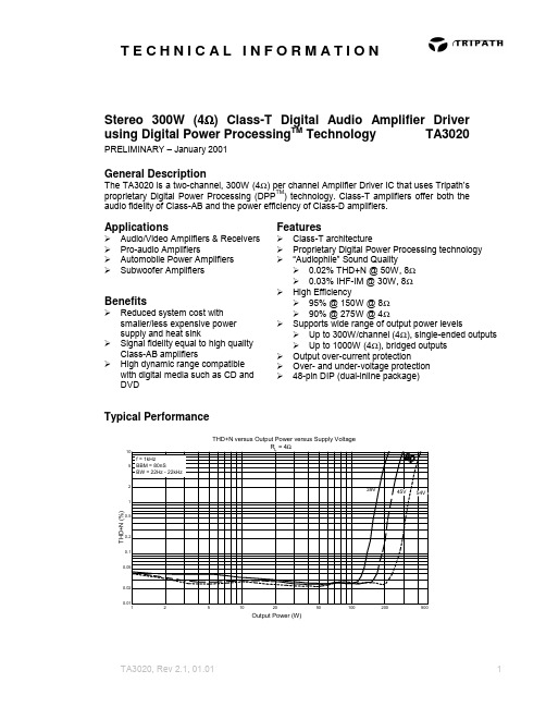
TECHNICAL INFORMATION
Stereo 300W (4Ω) Class-T Digital Audio Amplifier Driver using Digital Power ProcessingTM Technology TA3020
PRELIMINARY – January 2001
2
TA3020, Rev 2.1, 01.01
元器件交易网
TECHNICAL INFORMATION
Electrical Characteristics (Note 6)
TA = 25 °C. See Application/Test Circuit on page 7. Unless otherwise noted, the supply voltage is VPP=|VNN|=45V.
SYMBOL Iq PARAMETER Quiescent Current (No load, BBM0=1,BBM1=0, Mute = 0V) Mute Supply Current (No load, Mute = 5V) High-level input voltage (MUTE) Low-level input voltage (MUTE) High-level output voltage (HMUTE) IOH = 3mA Low-level output voltage (HMUTE) Output Offset Voltage Over Current Sense Voltage Threshold VPPSENSE Threshold Currents IOL = 3mA No Load, MUTE = Logic low 0.1% RFBA, RFBB, RFBC resistors TBD Over-voltage turn on (muted) Over-voltage turn off (mute off) Under-voltage turn off (mute off) Under-voltage turn on (muted) Over-voltage turn on (muted) Over-voltage turn off (mute off) Under-voltage turn off (mute off) Under-voltage turn on (muted) Over-voltage turn on (muted) Over-voltage turn off (mute off) Under-voltage turn off (mute off) Under-voltage turn on (muted) Over-voltage turn on (muted) Over-voltage turn off (mute off) Under-voltage turn off (mute off) Under-voltage turn on (muted) -TBD TBD TBD TBD TBD TBD TBD TBD TBD TBD 1.0 162 154 79 72 TBD TBD TBD TBD 174 169 86 77 TBD TBD TBD TBD 4.0 0.5 TBD TBD TBD TBD TBD TBD TBD TBD TBD TBD CONDITIONS VPP = +45V VNN = -45V V5 = 5V VN10 = 10V VPP = +45V VNN = -45V V5 = 5V VN10 = 10V 3.5 1.0 MIN. TYP. 90 90 45 200 1 1 20 1 MAX. UNITS mA mA mA mA mA mA mA mA V V V V mV V µA µA µA µA V V V V µA µA µA µA V V V V
4N38中文资料

Document Number Optocoupler, Phototransistor Output, With Base ConnectionFeatures•Isolation Test Voltage 5300 V RMS•Interfaces with common logic families•Input-output coupling capacitance < 0.5 pF •Industry Standard Dual-in line 6-pin package •Lead-free component•Component in accordance to RoHS 2002/95/EC and WEEE 2002/96/ECAgency Approvals•Underwriters Laboratory File #E52744 •DIN EN 60747-5-2 (VDE0884)DIN EN 60747-5-5 pending Available with Option 1ApplicationsAC mains detection Reed relay drivingSwitch mode power supply feedback Telephone ring detection Logic ground isolationLogic coupling with high frequency noise rejectionDescriptionThis data sheet presents five families of Vishay Indus-try Standard Single Channel Phototransistor Cou-plers.These families include the 4N35/ 4N36/ 4N37/4N38 couplers.Each optocoupler consists of gallium arsenide infra-red LED and a silicon NPN phototransistor.These couplers are Underwriters Laboratories (UL)listed to comply with a 5300 V RMS isolation test volt-age.This isolation performance is accomplished through Vishay double molding isolation manufacturing pro-cess. Comliance to DIN EN 60747-5-2(VDE0884)/DIN EN 60747-5-5 pending partial discharge isolation specification is available for these families by ordering option 1.These isolation processes and the Vishay ISO9001quality program results in the highest isolation perfor-mance available for a commecial plastic phototransis-tor optocoupler.The devices are available in lead formed configura-tion suitable for surface mounting and are available either on tape and reel, or in standard tube shipping containers.Note:Designing with data sheet is cover in Application Note 45Order InformationFor additional information on the available options refer to Option Information.PartRemarks4N35CTR > 100 %, DIP-64N36CTR > 100 %, DIP-64N37CTR > 100 %, DIP-64N38CTR > 20 %, DIP-64N35-X006CTR > 100 %, DIP-6 400 mil (option 6)4N35-X007CTR > 100 %, SMD-6 (option 7)4N35-X009CTR > 100 %, SMD-6 (option 9)4N36-X007CTR > 100 %, SMD-6 (option 7)4N36-X009CTR > 100 %, SMD-6 (option 9)4N37-X006CTR > 100 %, DIP-6 400 mil (option 6)4N37-X009CTR > 100 %, SMD-6 (option 9) Document Number 83717Absolute Maximum RatingsT amb = 25°C, unless otherwise specifiedStresses in excess of the absolute Maximum Ratings can cause permanent damage to the device. Functional operation of the device is not implied at these or any other conditions in excess of those given in the operational sections of this document. Exposure to absolute Maximum Rating for extended periods of the time can adversely affect reliability.InputOutputCouplerParameterTest conditionSymbol Value Unit Reverse voltage V R 6.0V Forward current I F 60mA Surge current ≤ 10 µsI FSM 2.5A Power dissipationP diss100mWParameterTest conditionSymbol Value Unit Collector-emitter breakdown voltageV CEO 70V Emitter-base breakdown voltageV EBO 7.0V Collector currentI C 50mA (t ≤ 1.0 ms)I C 100mA Power dissipationP diss150mWParameterTest conditionSymbol Value Unit Isolation test voltage V ISO5300V RMS Creepage ≥ 7.0mm Clearance≥ 7.0mm Isolation thickness between emitter and detector≥ 0.4mmComparative tracking index per DIN IEC 112/VDE0303,part 1175Isolation resistance V IO = 500 V, T amb = 25°C R IO 1012ΩV IO = 500 V, T amb = 100°CR IO 1011ΩStorage temperature T stg - 55 to + 150°C Operating temperature T amb - 55 to + 100°C Junction temperature T j 100°C Soldering temperaturemax. 10 s dip soldering: distance to seating plane ≥ 1.5 mmT sld260°CDocument Number Electrical CharacteristicsT amb = 25°C, unless otherwise specifiedMinimum and maximum values are testing requirements. Typical values are characteristics of the device and are the result of engineering evaluation. Typical values are for information only and are not part of the testing requirements.Input1) Indicates JEDEC registered valueOutput1)Indicates JEDEC registered valueCoupler1)Indicates JEDEC registered valueParameterT est conditionSymbol MinT yp.Max Unit Forward voltage 1)I F = 10 mAV F 1.3 1.5V I F = 10 mA, T amb = - 55°C V F 0.9 1.3 1.7V Reverse current 1)V R = 6.0 V I R 0.110µA CapacitanceV R = 0, f = 1.0 MHzC O25pFParameterT est conditionPart Symbol Min Typ.Max Unit Collector-emitter breakdown voltage 1)I C = 1.0 mA4N35BV CEO 30V 4N36BV CEO 30V 4N37BV CEO 30V 4N38BV CEO 80V Emitter-collector breakdown voltage 1)I E = 100 µABV ECO7.0V Collector-base breakdown voltage1)I C = 100 µA, I B = 1.0 µA4N35BV CBO 70V 4N36BV CBO 70V 4N37BV CBO 70V 4N38BV CBO 80VCollector-emitter leakage current1)V CE = 10 V, I F = 04N35I CEO 5.050nA 4N36I CEO 5.050nA V CE = 10 V, I F =04N37I CEO 5.050nA V CE = 60 V, I F = 04N38I CEO 50nA V CE = 30 V, I F = 0, T amb = 100°C4N35I CEO 500µA 4N36I CEO 500µA 4N37I CEO 500µA V CE = 60 V, I F = 0, T amb = 100°C4N38I CEO 6.0µA Collector-emitter capacitanceV CE = 0C CE6.0pFParameterT est conditionSymbol Min T yp.Max Unit Resistance, input to output 1)V IO = 500 V R IO 1011ΩCapacitance (input-output)f = 1.0 MHzC IO0.5pF Document Number 83717Current Transfer Ratio1)Indicates JEDEC registered valueSwitching Characteristics1) Indicates JEDEC registered valueTypical Characteristics (Tamb = 25 °C unless otherwise specified)ParameterTest conditionPart Symbol Min T yp.Max Unit DC Current Transfer Ratio 1)V CE = 10 V , I F = 10 mA4N35CTR DC 100%4N36CTR DC 100%4N37CTR DC 100%V CE = 10 V , I F = 20 mA 4N38CTR DC 20%V CE = 10 V , I F = 10 mA, T A = - 55 to + 100°C4N35CTR DC 4050%4N36CTR DC 4050%4N37CTR DC 4050%4N38CTR DC30%Parameter Test conditionSymbol Min Typ.Max Unit Switching time 1)I C = 2 mA, R L = 100 Ω, V CC = 10 Vt on , t off10µsFigure 1. Forward Voltage vs. Forward Currenti4n25_01100101.10.70.80.91.01.11.21.31.4I F -Forward Current -mAV F -F o r w a r d V o l t a g e -VFigure 2. Normalized Non-Saturated and Saturated CTR vs. LEDCurrenti4n25_020.00.51.01.5110100I F -LED Current -mAN C T R -N o r m l i z e d C T RDocument Number Figure 3. Normalized Non-saturated and Saturated CTR vs. LEDCurrent Figure 4. Normalized Non-saturated and saturated CTR vs. LEDCurrentFigure 5. Normalized Non-saturated and saturated CTR vs. LEDCurrenti4n25_030.00.51.01.5I F -LED Current -mAN C T R -N o r m a l i z e d C T Ri4n25_040.00.51.01.5I F -LED Current -mAN C T R -N o r m a l i z e d C T Ri4n25_050.00.51.01.5I F -LED Current -mAN C T R -N o r m a l i z e d C T RFigure 6. Collector-Emitter Current vs. Temperature and LEDCurrentFigure 7. Collector-Emitter Leakage Current vs.Temp.Figure 8. Normalized CTRcb vs. LED Current and Temp.i4n25_06605040302010I F -LED Current -mAI c e -C o l l e c t o r C u r r e n t -m Ai4n25_0710080604020–201010101010101010–2–1012345T A -Ambient Temperature -°CI c e o -C o l l e c t o r -E m i t t e r -n ATypicalV ce =10V i4n25_080.00.51.01.5I F -LED Current -mAN C T R c b -N o r m a l i z e d C T R c b.1110100 Document Number 83717Figure 9. Normalized Photocurrent vs. I F and Temp.Figure 10. Normalized Non-saturated HFE vs. Base Current andTemperatureFigure 11. Normalized HFE vs. Base Current and Temp.i4n25_090.0.011110I F -LED Current -mAN o r m a l i z e d P h o t o c u r r e n t.1110100i4n25_100.40.61.01.2Ib -Base Current -µAN H F E -N o r m a l i z e d H F E0.8i4n25_110.00.51.01.5N H F E (s a t )-N o r m a l i z e d S a t u r a t e d H F E1101001000Ib -Base Current -µAFigure 12. Propagation Delay vs. Collector Load ResistorFigure 13. Switching TimingFigure 14. Switching Schematici4n25_121000RL -Collector Load Resistor -k Ωt P L H -P r o p a ga t i o n D e l a y -µs.1110100t P H L -P r o p a g a t i o n D e l a y -µsi4n25_13I FV i4n25_14V =5.0VF=10V OI F =10mAPackage Dimensions in Inches (mm)For 4N35/36/37/38..... see DIL300-6 Package dimension in the Package Section.For products with an option designator (e.g. 4N35-X006 or 4N36-X007)..... see DIP-6 Package dimensions in the Package Section. DIL300-6 Package DimensionsDocument Number Document Number 83717Ozone Depleting Substances Policy StatementIt is the policy of Vishay Semiconductor GmbH to1.Meet all present and future national and international statutory requirements.2.Regularly and continuously improve the performance of our products, processes, distribution andoperatingsystems with respect to their impact on the health and safety of our employees and the public, as well as their impact on the environment.It is particular concern to control or eliminate releases of those substances into the atmosphere which are known as ozone depleting substances (ODSs).The Montreal Protocol (1987) and its London Amendments (1990) intend to severely restrict the use of ODSs and forbid their use within the next ten years. Various national and international initiatives are pressing for an earlier ban on these substances.Vishay Semiconductor GmbH has been able to use its policy of continuous improvements to eliminate the use of ODSs listed in the following documents.1.Annex A, B and list of transitional substances of the Montreal Protocol and the London Amendmentsrespectively2.Class I and II ozone depleting substances in the Clean Air Act Amendments of 1990 by the EnvironmentalProtection Agency (EPA) in the USA3.Council Decision 88/540/EEC and 91/690/EEC Annex A, B and C (transitional substances) respectively. Vishay Semiconductor GmbH can certify that our semiconductors are not manufactured with ozone depleting substances and do not contain such substances.We reserve the right to make changes to improve technical designand may do so without further notice.Parameters can vary in different applications. All operating parameters must be validated for each customer application by the customer. Should the buyer use Vishay Semiconductors products for any unintended or unauthorized application, the buyer shall indemnify Vishay Semiconductors against all claims, costs, damages, and expenses, arising out of, directly or indirectly, any claim of personal damage, injury or death associated with such unintended or unauthorized use.Vishay Semiconductor GmbH, P.O.B. 3535, D-74025 Heilbronn, GermanyTelephone: 49 (0)7131 67 2831, Fax number: 49 (0)7131 67 2423Document Number 。
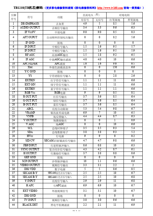
东芝芯片资料
0 900Ω 600Ω 19.5K 15K 13K 19K
LA7833引脚功能
引脚
1 2 3 4 4 6 7
功能
接地端 场输出 自举升压电源端 场激励输入 负反馈输入及相位补偿 电源端 场逆程脉冲输出
直流电压
0V 13.6V 25.5V 0.8V 0.8V 26V 1.4V
纹波滤波电路引脚 第二伴音中频输出 调频直流反馈滤波电路引脚
电压
1.8V 0V 1.3V
+2.5V
+5V 2.45V 2.45V
1V 6.4V 0V 0V 2.3V 1.6V 0V +5V 3.6V 4.3V 0V 8V 8.8V 3.5V 5.6V 3.4V 3.5V
RXIK档对地电阻(黑表笔接地)
场AGC 总线时钟端子 总线数据端子
行电源 SECAM识别/载波信号输出
行逆程脉冲输入 复合同步信号输出 行激励信号输出
接地 沙堡脉冲输出 视频信号输出
数字电源
SECAM蓝色差信号输入 SECAM红色差信号输入
亮度信号输入 行AFC滤波
外接视频信号
接地 视频信Leabharlann 输入黑电平检测滤波直流电压(V)
有信号 4.9
800Ω 0
12.5K
12.8K
6K 13K 13K 13K 12.8K 13.2K
0 12.8K 13K 11.5K
1K 12.5K 12K
0 900Ω 600Ω 12.5K 12.2K 11.5K 12K
红笔接地 R×1K档
800Ω 0
19K
27K
5.5K 20K 20K 18K 28K 28K
TSOP1838中文手册
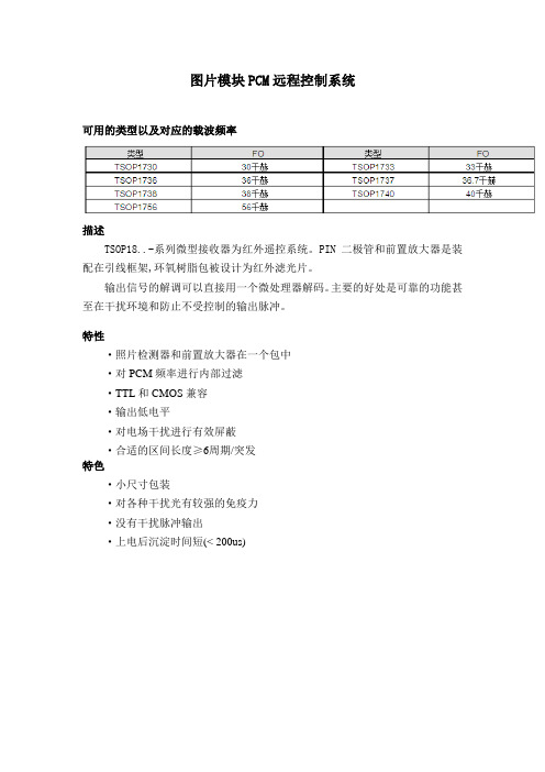
图片模块PCM远程控制系统可用的类型以及对应的载波频率描述TSOP18..-系列微型接收器为红外遥控系统。
PIN二极管和前置放大器是装配在引线框架,环氧树脂包被设计为红外滤光片。
输出信号的解调可以直接用一个微处理器解码。
主要的好处是可靠的功能甚至在干扰环境和防止不受控制的输出脉冲。
特性·照片检测器和前置放大器在一个包中·对PCM频率进行内部过滤·TTL和CMOS兼容·输出低电平·对电场干扰进行有效屏蔽·合适的区间长度≥6周期/突发特色·小尺寸包装·对各种干扰光有较强的免疫力·没有干扰脉冲输出·上电后沉淀时间短(< 200us)框图绝对最大额定值(amb T = 25℃)参数 测试条件 符号值单位 电源电压 (2脚) S V -0.3---6.0 V 电源电压 (2脚) S V 5mA 输出电压 (引脚3) O V -0.3---6.0 V 输出电流 (引脚3) O I 5 mA 结温J T100 ℃ 存储温度范围 stg T -25------85 ℃ 工作温度范围amb T -25------85 ℃ 耗电量 amb T ≤85℃ tot P 50 mW 焊接温度10≤t ssd T260℃基本特点( amb T = 25℃)参数测试条件符号 最小 典型 最大 单位 电源电流(引脚3)0v 5v ==E V S ,SD I0.9 1.2 1.5 mAklx 40,5==V S E V V sunlight SH I1.3 电源电压(引脚3) S V 4.5 5.5 V 传输距离 V E V 0=,测试信号参见图7d 35 m 输出电压(引脚1)o2e f f m /m 7.0E mA 5.0===,,W I O SLOSL V250mV辐照度(30至40KHZ) 脉冲宽度公差:o pi po o pi f t t f /6/4t +<<-min e E 0.3 0.5 2/m mW辐照度(56KHZ ) 0.4 0.7 辐照度max e E302m /W方向性 传输距离的半角 2/1φ45±deg应用电路*)建议,抑制电源干扰合适的数据格式TSOP18电路是这样设计的:避免由于噪声或干扰造成的异常输出脉冲。
- 1、下载文档前请自行甄别文档内容的完整性,平台不提供额外的编辑、内容补充、找答案等附加服务。
- 2、"仅部分预览"的文档,不可在线预览部分如存在完整性等问题,可反馈申请退款(可完整预览的文档不适用该条件!)。
- 3、如文档侵犯您的权益,请联系客服反馈,我们会尽快为您处理(人工客服工作时间:9:00-18:30)。
IR Receiver Modules for Remote Control SystemsTSOP392.., TSOP394.. Vishay SemiconductorsMECHANICAL DATA Pinning:1 = OUT,2 = V S,3 = GND FEATURES•Very low supply current•Photo detector and preamplifier in one package •Internal filter for PCM frequency•Improved shielding against EMI•Supply voltage: 2.5 V to 5.5 V•Improved immunity against ambient light•Insensitive to supply voltage ripple and noise •Component in accordance to RoH S 2002/95/EC and WEEE 2002/96/ECDESCRIPTIONThe TSOP392.., TSOP394.. series are miniaturized receivers for infrared remote control systems. A PIN diode and a preamplifier are assembled on a lead frame, the epoxy package acts as an IR filter.The demodulated output signal can be directly decoded by a microprocessor. The TSOP392.. is compatible with all common IR remote control data formats. The TSOP394.. is optimized to suppress almost all spurious pulses from energy saving fluorescent lamps but will also suppress some data signals.This component has not been qualified according to automotive specifications.BLOCK DIAGRAM APPLICATION CIRCUIT19026PARTS TABLECARRIER FREQUENCY STANDARD APPLICATIONS (AGC2/AGC8)VERY NOISY ENVIRONMENTS (AGC4) 30 kHz TSOP39230TSOP3943033 kHz TSOP39233TSOP3943336 kHz TSOP39236TSOP3943638 kHz TSOP39238TSOP3943840 kHz TSOP39240TSOP3944056 kHz TSOP39256TSOP39456TSOP392.., TSOP394..IR Receiver Modules for Remote Control SystemsVishay SemiconductorsNote(1)Stresses beyond those listed under “Absolute Maximum Ratings” may cause permanent damage to the device. This is a stress rating only and functional operation of the device at these or any other conditions beyond those indicated in the operational sections of this specification is not implied. Exposure to absolute maximum rating condtions for extended periods may affect the device reliability.Note (1)T amb = 25°C, unless otherwise specifiedTYPICAL CHARACTERISTICST amb = 25°C, unless otherwise specifiedFig. 1 - Output Active LowFig. 2 - Pulse Length and Sensitivity in Dark AmbientABSOLUTE MAXIMUM RATINGS (1)PARAMETER TEST CONDITIONSYMBOLVALUE UNIT Supply voltage (pin 2)V S - 0.3 to + 6.0V Supply current (pin 2)I S 3mA Output voltage (pin 1)V O - 0.3 to (V S + 0.3)V Output current (pin 1)I O 5mA Junction temperatureT j 100°C Storage temperature range T stg - 25 to + 85°C Operating temperature range T amb - 25 to + 85°C Power consumption T amb ≤ 85°C P tot 10mW Soldering temperaturet ≤ 10 s, 1 mm from case T sd260°CELECTRICAL AND OPTICAL CHARACTERISTICS (1)PARAMETER TEST CONDITION SYMBOL MIN.TYP.MAX.UNIT Supply current (pin 2)E v = 0, V S = 3.3 V I SD 0.270.350.45mA E v = 40 klx, sunlightI SH 0.45mA Supply voltage V S 2.55.5V Transmission distance E v = 0, test signal see fig. 1,IR diode TSAL6200,I F = 250 mA d 45m Output voltage low (pin 1)I OSL = 0.5 mA, E e = 0.7 mW/m 2,test signal see fig. 1V OSL 100mV Minimum irradiance Pulse width tolerance:t pi - 5/f o < t po < t pi + 6/f o ,test signal see fig. 1E e min.0.150.35mW/m 2Maximum irradiance t pi - 5/f o < t po < t pi + 6/f o ,test signal see fig. 1E e max.30W/m 2DirectivityAngle of half transmission distanceϕ1/2± 45degE eV O V VTSOP392.., TSOP394..Vishay SemiconductorsIR Receiver Modules for Remote Control SystemsFig. 3 - Output FunctionFig. 4 - Output Pulse DiagramFig. 5 - Frequency Dependence of ResponsivityFig. 6 - Sensitivity in Bright AmbientFig. 7 - Sensitivity vs. Supply Voltage DisturbancesFig. 8 - Sensitivity vs. Electric Field DisturbancesE eV O V V OL0.00.20.40.60.81.01.20.70.9 1.1 1.3f/f 0 - Relati v e Fre qu ency16925E /E - R e l. R e s p o n s i v i t y e m i n.eTSOP392.., TSOP394.. IR Receiver Modules forRemote Control SystemsVishay SemiconductorsFig. 9 - Maximum Envelope Duty Cycle vs. Burst Length Fig. 10 - Sensitivity vs. Ambient Temperature Fig. 11 - Relative Spectral Sensitivity vs. WavelengthFig. 12 - Horizontal DirectivityFig. 13 - Vertical Directivity Fig. 14 - Sensitivity vs. Supply VoltageTSOP392.., TSOP394..Vishay SemiconductorsIR Receiver Modules for Remote Control SystemsSUITABLE DATA FORMATThe TSOP392.., TSOP394.. series are designed to suppress spurious output pulses due to noise or disturbance signals.Data and disturbance signals can be distinguished by the devices according to carrier frequency, burst length and envelope duty cycle. The data signal should be close to the band-pass center frequency (e.g. 38 kH z) and fulfill the conditions in the table below.When a data signal is applied to the TSOP392.., TSOP394..in the presence of a disturbance signal, the sensitivity of the receiver is reduced to insure that no spurious pulses are present at the output. Some examples of disturbance signals which are suppressed are:•DC light (e.g. from tungsten bulb or sunlight)•Continuous signals at any frequency•Strongly or weakly modulated noise from fluorescent lamps with electronic ballasts (see figure 15 or figure 16)Fig. 15 - IR Signal from Fluorescent Lampwith Low ModulationFig. 16 - IR Signal from Fluorescent Lampwith High ModulationNoteFor data formats with short bursts please see the datasheet for TSOP391.., TSOP393..0101520Time (ms)16920I R S i g n a l50101520Time (ms)16921I R S i g n a l10TSOP392..TSOP394..Minimum burst length10 cycles/burst 10 cycles/burst After each burst of lengtha minimum gap time is required of10 to 70 cycles ≥ 10 cycles 10 to 35 cycles ≥ 10 cycles For bursts greater thana minimum gap time in the data stream is needed of 70 cycles > 4 x burst length35 cycles> 10 x burst lengthMaximum number of continuous short bursts/second 18001500Compatible to NEC code yes yes Compatible to RC5/RC6 code yes yes Compatible to Sony codeyes no Compatible to Thomson 56 kHz codeyes yes Compatible to Mitsubishi code (38 kHz, preburst 8 ms, 16 bit)yes no Compatible to Sharp codeyesyesSuppression of interference from fluorescent lampsMost common disturbance signals are suppressedEven extreme disturbance signals are suppressedTSOP392.., TSOP394..IR Receiver Modules forVishay SemiconductorsRemote Control SystemsPACKAGE DIMENSIONS in millimetersTSOP392.., TSOP394..Vishay Semiconductors IR Receiver Modules forRemote Control SystemsOZONE DEPLETING SUBSTANCES POLICY STATEMENTIt is the policy of Vishay Semiconductor GmbH to1.Meet all present and future national and international statutory requirements.2.Regularly and continuously improve the performance of our products, processes, distribution and operating systems withrespect to their impact on the health and safety of our employees and the public, as well as their impact on the environment. It is particular concern to control or eliminate releases of those substances into the atmosphere which are known as ozone depleting substances (ODSs).The Montreal Protocol (1987) and its London Amendments (1990) intend to severely restrict the use of ODSs and forbid their use within the next ten years. Various national and international initiatives are pressing for an earlier ban on these substances. Vishay Semiconductor GmbH has been able to use its policy of continuous improvements to eliminate the use of ODSs listed in the following documents.1.Annex A, B and list of transitional substances of the Montreal Protocol and the London Amendments respectively.2.Class I and II ozone depleting substances in the Clean Air Act Amendments of 1990 by the Environmental Protection Agency(EPA) in the USA.3.Council Decision 88/540/EEC and 91/690/EEC Annex A, B and C (transitional substances) respectively.Vishay Semiconductor GmbH can certify that our semiconductors are not manufactured with ozone depleting substances and do not contain such substances.We reserve the right to make changes to improve technical designand may do so without further notice.Parameters can vary in different applications. All operating parameters must be validated for each customer application by the customer. Should the buyer use Vishay Semiconductors products for any unintended or unauthorized application, the buyer shall indemnify Vishay Semiconductors against all claims, costs, damages, and expenses, arising out of, directly or indirectly, any claim of personal damage, injury or death associated with such unintended or unauthorized use.Vishay Semiconductor GmbH, P.O.B. 3535, D-74025 Heilbronn, GermanyDisclaimer Legal Disclaimer NoticeVishayAll product specifications and data are subject to change without notice.Vishay Intertechnology, Inc., its affiliates, agents, and employees, and all persons acting on its or their behalf (collectively, “Vishay”), disclaim any and all liability for any errors, inaccuracies or incompleteness contained herein or in any other disclosure relating to any product.Vishay disclaims any and all liability arising out of the use or application of any product described herein or of any information provided herein to the maximum extent permitted by law. The product specifications do not expand or otherwise modify Vishay’s terms and conditions of purchase, including but not limited to the warranty expressed therein, which apply to these products.No license, express or implied, by estoppel or otherwise, to any intellectual property rights is granted by this document or by any conduct of Vishay.The products shown herein are not designed for use in medical, life-saving, or life-sustaining applications unless otherwise expressly indicated. Customers using or selling Vishay products not expressly indicated for use in such applications do so entirely at their own risk and agree to fully indemnify Vishay for any damages arising or resulting from such use or sale. Please contact authorized Vishay personnel to obtain written terms and conditions regarding products designed for such applications.Product names and markings noted herein may be trademarks of their respective owners.元器件交易网。