BYW82中文资料
HT85XXX中文资料
HT85XXX Green VoiceTM
Features
· Operating voltage: 2.4V~5.0V · Driver speaker (32W) VDD=4.5V,
IDD=90mA · Programmable tone melody generator · ADPCM, m-law PCM, PCM synthesis · Wide range of sampling rate for voice
Supply Voltage.................................-0.3V to 6V Input Voltage .................VSS-0.3V to VDD+0.3V
Storage Temperature.................-50°C to 125°C Operating Temperature ..............-20°C to 70°C
21, 22 VSS
¾
¾
Negative power supply, ground
23
OSC
I
¾
Built-in RC oscillator An oscillator resistor is connected between OSC and VSS
Absolute Maximum Ratings
Pin No.
Pin Name
I/O
Internal Connection
Description
1, 2, 8, 24~28
NC
¾
¾
No connection
3, 4, 5
PP0, PDA, PP1
LM98555CCMHXNOPB;LM98555CCMHNOPB;中文规格书,Datasheet资料

LM98555LM98555 CCD DriverLiterature Number: SNAS290CLM98555 CCD DriverGeneral DescriptionThe LM98555 is a highly integrated driver circuit intended for CCD driving applications. It combines 25 drivers of varying drive strengths into one chip to provide a complete CCD driv-ing solution. Due to this one-chip integration, optimal skew control is achieved for this demanding application. Features■All CCD drivers integrated into one package■High strength drivers designed specifically for CCD loads ■Ability to scale clock driver strength■Skew specifications guaranteed■Separate input and output power supplies ■CMOS process technology■64-pin TSSOP package with extended power handling capabilityKey SpecificationsSupply Voltage Inputs 3.0 to 5.5VDrivers 4.5 to 5.8V Maximum Output Skew Between P1Aand P2Aoutputs0.5 nsMaximum PowerHandling2.0WFunctional Description20126401FIGURE 1. Functional Block DiagramTRI-STATE® is a registered trademark of National Semiconductor Corporation.© 2007 National Semiconductor 98555 CCD DriverCommercial Temperature RangeNS PackageLM98555CCMH64-Pin Exposed Pad TSSOPConnection Diagram20126402FIGURE 2. TSSOP Package Pinout 2L MSymbol Pin Type DescriptionDriver inputsP2BIN8Input CMOS logic input for the P2B driver.RSIN9Input CMOS logic input for the RS driver.CPIN10Input CMOS logic input for the CP driver.P1AIN15Input CMOS logic input for the P1A ganged (8) driver set.P2AIN18Input CMOS logic input for the P2A ganged (8) driver set.SHIN21Input CMOS logic input for the SH ganged (3) driver set.AFEIN22Input CMOS logic input for the AFE driver.MCLIN23Input CMOS logic input for the MCL driver.SHDIN24Input CMOS logic input for the SHD driver.Driver OutputsSHDOUT28Output; Low-Strength Driver output for the SHDINinput signal.MCLOUT30Output; Low-Strength Driver output for the MCLINinput signal.AFEOUT31Output; Low-Strength Driver output for the AFEINinput signal.CPOUT2Output; Low-Strength Driver output for the CPINinput signal. Typically used to drive the Clamp Gate input of the CCD.RSOUT3Output; Low-Strength Driver output for the RSINinput signal. Typically used to drive the Reset Gate input of the CCD.P2BOUT5Output; Low-Strength Driver output for the P2BINinput signal.P2AOUT047Output; TRI-STATE®; High-Strength Ganged driver outputs for the P2AINinput. Typically the user may join together these outputs to drive the φ2 clock input of the CCD. Some of these outputs may be disabled using the EN(1:0) inputs - see the Functional Description section.P2AOUT146P2AOUT243P2AOUT342P2AOUT439P2AOUT538P2AOUT635P2AOUT734P1AOUT050Output; TRI-STATE; High-Strength Ganged driver outputs for the P1AINinput. Typically the user may join together these outputs to drive the φ1 clock input of the CCD. Some of these outputs may be disabled using the EN(1:0) inputs - see the Functional Description section.P1AOUT151P1AOUT254P1AOUT355P1AOUT458P1AOUT559P1AOUT662P1AOUT763SHOUT026Output; Low-Strength Ganged driver outputs for the SHINinput signal. Typically used to drive the Shift Gate input of the CCD.SHOUT127SHOUT26Logic InputsEN011Input Driver enable control. Some of the P1A and P2A drivers can be disabled usingthese inputs. See the Functional Description section.EN112555Power & Ground Pins V DDI141620PowerV DD for pre-drivers.V DDO17293237404549535760PowerV DD for final-stage driver.GND I131719Ground Ground connection for all circuitry other than the Final-Stage Drivers.GND O425333641444852566164Ground Ground connection for the Final-Stage Drivers. 4L MIf Military/Aerospace specified devices are required, please contact the National Semiconductor Sales Office/ Distributors for availability and specifications.Supply Voltage−0.5V to 6.2V Package Power Rating at 25°C(Note 2) 2.0 Watts Voltage on Any Input or Output Pin−0.5V to VDD+0.5V DC Input Current at Any Pin25 mA DC Package Input Current50 mA Storage Temperature−65°C to +150°C Lead temperature (Soldering, 10 sec.)300°C ESD SusceptibilityHuman Body Model2000V Machine Model200V Operating ConditionsSupply VoltageVDDI+3.0V to +5.5V Supply VoltageVDDO+4.5V to +5.8VSupply Sequencing(Note 3)VDDI < VDDO+0.2VAmbient Temperature (TA)0 to 70°C Operating Frequency30 MHz Power Dissipation (Note 4) 2.0W Package Thermal Resistances PackageθJ-A(Note 5)θJ-PAD(Thermal Pad) 64-Lead ExposedPad TSSOP36.8°C / W 6.2°C / WDC Electrical CharacteristicsThe following specifications apply for GND = 0V, VDDI = 3.3V, VDDO= 5.0V, unless noted otherwise. Boldface limits apply forT A = TMINto TMAX; all other limits TA= 25°CSymbol Parameter Conditions Min Typical Max UnitsI I Logic 1 Input Current VI= VDDI-10.0041µALogic 0 Input Current VI= GNDI-10.0061µAV IT Input Threshold VDDI= 3.3V 1.41 1.57 1.75VInput Threshold VDDI= 5.0V 2.48VInput Threshold Hysteresis VDDI= 3.3V-7211100mVΔV IT Input Threshold Variation Between P1A, P2A inputs-100100mVROOutput Impedance P1A and P2AOutputs ILOAD= 525 mA6.19.9ΩRO= (VDDO- VO)/IOHorRO= VO/IOLROOutput Impedance All OtherOutputs ILOAD= 280 mA10.217.4ΩRO= (VDDO- VO)/IOHorRO= VO/IOL555The following specifications apply for GND = 0V, V DDI = 3.3V, V DDO = 5.0V, unless noted otherwise. Boldface limits apply for T A = T MIN to T MAX ; all other limits T A = 25°C Symbol ParameterConditionsMin Typical Max Unit PHL Prop Delay: High-to-Low P1A and P2A Outputs C L = 220 pF, R L = 10Ω(Note 6)3.064.66.55nst PHLProp Delay: High-to-Low CP, RS, P2B Outputs C L = 82 pF, R L = 10Ω(Note 6)(Note 8)4.1nst PLH Prop Delay: Low-to-High P1A and P2A Outputs C L = 220 pF, R L = 10Ω(Note 7)3.384.96.68nst PLHProp Delay: Low-to-High CP, RS, P2B Outputs C L = 82 pF, R L = 10Ω(Note 7)(Note 8)4.2nst SKEWProp Delay Skew High-to-Low Between any P1A or P2A Outputs on a Single UnitC L = 220 pF, R L = 10Ω109387psProp Delay Skew Low-to-High157490Important Note: Not all drivers can be loaded to the highest specified load at the same time without violating the maximum power dissipation limit. The syst design must guarantee that the maximum power dissipation specification is never exceeded.Note 1:Absolute maximum ratings are those values beyond which the safety of the device cannot be guaranteed. They are not meant to imply that the devic should be operated at these limits.Note 2:Package power rating assumes the exposed thermal pad is soldered to the printed circuit board as recommended, with significant heat spreading provid by vias to internal or bottom heat dissipation planes or pad. If this is not the case, then the package power rating should be reduced. See the Thermal Guidelin in the applications section for more information.Note 3:When powering up and down, transient voltage levels on V DDI must be lower than (V DDO + 0.2V)Note 4:This is the power dissipated on-chip due to all currents flowing through the device - both DC and AC. This operating condition will be violated if all dri outputs are fully loaded and operating at the same time at the rated F MAX . The system design must constrain the chip's operating conditions (loads, power supp number of parallel drivers enabled, frequency of operation) to make certain that this limit is never exceeded.Note 5:Package thermal resistance for junction to ambient is based on a 5.5 inch by 3 inch, 4 layer printed circuit board, with thermal vias connecting the he sinking pad to a full internal ground plane. Tests were done in still air, with a power dissipation of 2.0 W, at an ambient temperature of 22°C.Note 6:Propagation Delay High-to-Low with output low trigger voltage at V DDO *0.75.Note 7:Propagation Delay Low-to-High with output high trigger voltage at V DDO *0.25.Note 8:Typical values determined from characterization testing only. Not production tested or guaranteed.Test Conditions20126403FIGURE 3. AC Test Conditions 6L MThe LM98555 is a fully integrated clock driver/buffer for high speed CCD applications. It provides high performance low impedance drivers, with optimized low skew performance of the P1 and P2 outputs. Enable inputs allow use of two, four,six, or all eight P1 and P2 drivers to optimize the amount of drive for the application. The 64 pin thermally enhanced TSSOP provides excellent power handling through the use of an exposed heat transfer pad on the underside of the pack-age.THERMAL GUIDELINESThe LM98555's maximum power dissipation limit, shown in the Operating Conditions section, must be strictly adhered to.The product's multiple high-strength drivers, with their ability to drive a wide-range of loads, make it possible to be within spec on each output and yet violate the aggregate maximum power dissipation limit for the total product. Special caution must be paid to this by limiting the chip's operating conditions (loads, power supply, number of parallel drivers enabled, fre-quency of operation) to make certain that the maximum power dissipation limit is never exceeded.Thermal characterization of the device has been done to pro-vide reference points under specific conditions. θ junction to ambient was measured using a 5.5 inch by 3 inch, 4 layer PCB. The thermal contact pad on the board was connected using vias to a full ground plane on one of the internal layers.The recommended thermal pad is shown in Figure 4.20126406FIGURE 4. Exposed Pad Land PatternThe vias shown provide a path for heat to flow from the pad to a heat sinking or dissipating area of the printed circuit board. The following figures show several typical examples of how this can be done, and illustrate how heat is conducted away from the IC to larger areas where it is dissipated.20126407FIGURE 5. 4 Layer PCB - Example 120126409FIGURE 6. 4 Layer PCB - Example 220126408FIGURE 7. 2 Layer PCB555mal pad to this ground plane with vias will usually provide adequate heat management. In 2 layer boards, it is important to provide a large heat spreading pad on the opposite side of the board. The vias will provide a good thermal connection between the pad under the IC, and the heat spreading pad on the bottom of the board. Thermal modelling can be done using the θ junction to pad information provided, to calculate the required area of copper based on the ambient temperature of the system, and the calculated amount of thermal dissipation in the LM98555.POWER DISSIPATIONThe amount of power dissipated in the device can be deter-mined by considering the following factors:•Power dissipated delivering energy to the load capacitance•Power dissipated delivering energy to parasitic capacitance•Power dissipated due to leakage in the ICThe amount of power dissipated due to leakage is very small in this CMOS device. Most of the power will be due to the load capacitance being switched, with a small additional amount caused by the parasitic capacitance of the output circuitry,output pins, and PCB traces. A typical parasitic capacitance would be on the order of 5 pF. Since the load capacitance will be on the order of 100 pF or more, this usually dominates the power dissipation calculation. The following equation can be used to calculate the power dissipation due to capacitive switching of the loads:P = Sum[Output Frequency x Load Capacitance x Output Voltage Squared] (summed for all outputs)INPUT SIGNALSCare should be taken to match the trace lengths between timing signals that require low skew. Usually, the P1A and P2A signals will be the most critical. In some applications, the timing of P2B with respect to P1A and P2A can also be im-portant, and that input trace should also be carefully de-signed.Trace shape and width should also be carefully controlled.The trace geometry will determine the characteristic impedance of each trace. The impedance should be set to give reasonable immunity to noise coupling into the trace.With a known trace impedance, the signals can be terminated using a series resistor at the source that is equal to the char-acteristic impedance. This will provide a signal with minimum overshoot and ringing, and will contribute to better perfor-mance of the final signal reaching the CCD.OUTPUT CONNECTIONS AND LOADING EXAMPLES The LM98555 can be used with a wide variety of different CCD sensors. The P1Aoutx and P2Aoutx outputs can be se-lectively enabled to provide 2, 4, 6, or 8 drivers. This allows the available drive strength to be optimized for the sensor and application. Connecting multiple outputs together in parallel as shown in the typical application circuit provides lower drive impedance as needed to suit the load being driven. When driving smaller loads, lower switching noise will be generated if the minimum necessary outputs are enabled and used.The output signal traces should also be designed for a known impedance. Source terminating resistors should be used in series with each output to provide good matching to the trace characteristic impedance. The resistors should be located asbe combined after the termination resistors. This will provi the best summing of adjacent outputs. The combined sign should then pass through an EMI type ferrite bead. This co ponent can be selected to change the bandwidth or shape the clocking signal to achieve the best CCD transfer efficie cy.Several other techniques will also help maintain signal quali and minimize timing differences between critical signals. Vi should not be used for critical timing signals. These can a impedance discontinuities that will affect the waveform qu ity. Traces should have gradual bends and avoid sha changes in direction that can also introduce impedance d continuities.SELECTIVE DRIVER ENABLINGWith the Enable pins, the user has the capability to enab only the drivers that are required for the application, th eliminating unnecessary outputs switching. The following ble shows the details.EN1EN0Driver-set State00P1Aout(1:0) and P2Aout(1:0) are enabled; a others disabled.01P1Aout(3:0) and P2Aout(3:0) are enabled; a others disabled.10P1Aout(5:0) and P2Aout(5:0) are enabled; a others disabled.11All P1Aout and P2Aout drivers are enabled.Note: The disabled drivers' outputs are in TRI-STATE.POWER SUPPLY SEQUENCINGDuring device power-up and power-down, V DDI must be ma tained less than (V DDO + 0.2V) to prevent excessive curre flow through the internal ESD protection circuitry. Since mo applications will involve 3V on V DDI and 5V on V DDO , this c be easily met. If this voltage relationship cannot be met, th the DC pin and package limits for input current must be ma tained by controlling the source impedance of the V DDI suppPOWER AND GROUND - PLANES VERSUS BUSES The best performance will be achieved by using planes rath than traces for power and ground. Planes provide lower ele trical and thermal impedance. Ground bounce and ringing a reduced, electromagnetic emissions are minimized and t best thermal performance will be realized.A single common ground plane should be used for all pow and signal domains.Another circuit board layer can be used to provide power the various circuitry. Different power buses can be provid by isolated planes within this layer of the circuit board.EMI MANAGEMENTGood EMI control will be achieved by addressing the followi items:•Provide proper source termination of output signals •Limit length of output traces•Ensure adequate power supply decoupling•Provide power and ground planes as much as possible •Provide common ground plane for all signals, especiall between LM98555 outputs and load CCD•Enable and use the minimum number of outputs neede 8L M64-TSSOPNS Package Number MXD64A 555分销商库存信息:NATIONAL-SEMICONDUCTORLM98555CCMH/NOPB LM98555CCMHX/NOPB。
ES18E18-P1J中文资料(Mean Well)中文数据手册「EasyDatasheet - 矽搜」

直流电压
Note.2 3.3V
5V
7.5V
9V
12V
15V
18V
24V
28V
48V
额定电流
2.72A 3.0A
2.0A
2.0A
1.50A 1.20A 1.0A
0.75A 0.64A 0.375A
电流范围
0.3 ~ 2.72A 0.3 ~ 3.0A 0.3 ~ 2.0A 0.2 ~2.0A 0.15 ~ 1.50A 0.1 ~ 1.20A 0.1 ~ 1.0A 0.1 ~ 0.75A 0.06 ~ 0.64A 0.05 ~ 0.375A
漏电流(最大)
0.25mA / 240VAC
保护
过载
过电压
工作温度.
工作湿度
110 ~ 200% rated output power
130 ~ 350% rated output power
Protection type : Hiccup mode, recovers automatically after fault condition is removed
额定功率(最大)
Байду номын сангаас9W
15W
15W
18W
18W
18W
18W
18W
18W
18W
输出
纹波及噪音(最大) Note.3 50mVp-p 50mVp-p 80mVp-p 80mVp-p 80mVp-p 100mVp-p 150mVp-p 180mVp-p 240mVp-p 240mVp-p
电压 ADJ.范围
Fixed
电压容差
Note.4 5.0%
5.0%
82C87中文资料

82C87HCMOS Octal Inverting Bus TransceiverFile Number2978.1March 1997Features•Full Eight Bit Bi-Directional Bus Interface •Industry Standard 8287 Compatible Pinout•High Drive Capability- B Side I OL . . . . . . . . . . . . . . . . . . . . . . . . . . . . . .20mA - A Side I OL . . . . . . . . . . . . . . . . . . . . . . . . . . . . . .12mA •Three-State Inverting Outputs•Propagation Delay . . . . . . . . . . . . . . . . . . . . .35ns Max.•Gated Inputs-Reduce Operating Power-Eliminate the Need for Pull-Up Resistors •Single 5V Power Supply•Low Power Operation . . . . . . . . . . . . . . .ICCSB = 10µA •Operating Temperature Range-C82C87H . . . . . . . . . . . . . . . . . . . . . . . . .0o C to +70o C -I82C87H. . . . . . . . . . . . . . . . . . . . . . . .-40o C to +85o C -M82C87H. . . . . . . . . . . . . . . . . . . . . .-55o C to +125o CDescriptionThe Intersil 82C87H is a high performance CMOS Octal T ransceiver manufactured using a self-aligned silicon gate CMOS process (Scaled SAJI IV). The 82C87H provides a full eight-bit bi-directional bus interface in a 20 pin package. The T ransmit (T) control determines the data direction. The active low output enable (OE) permits simple interface to the 80C86, 80C88 and other microprocessors. The 82C87H has gated inputs, eliminating the need for pull-up/pull-down resis-tors and reducing overall system operating power dissipation.The 82C87H provides inverted data at the outputs.Ordering InformationPART NUMBERS PACK-AGETEMP.RANGE PKG.NO.5MHz 8MHzCP82C87H-5CP82C87H 20 LdPDIP0o C to +70o CE20.3IP82C87H-5IP82C87H-40o C to +85o C E20.3CS82C87H-5CS82C87H 20 LdPLCC0o C to +70o CN20.35IS82C87H-5IS82C87H-40o C to +85o C N20.35CD82C87H-5CD82C87H 20 LdCERDIP 0o C to +70o CF20.3ID82C87H-5ID82C87H-40o C to +85o C F20.3MD82C87H-5/B --55o C to +125o CF20.35962-8757702RA -SMD #F20.3MR82C87H-5/B -20 Pad CLCC -55o C to +125o CJ20.A 5962-87577022A-SMD #J20.ACAUTION: These devices are sensitive to electrostatic discharge; follow proper IC Handling Procedures.Pinouts82C87H (PDIP, CERDIP)TOP VIEW82C87H (PLCC, CLCC)TOP VIEW1112131415161718201910987654321A0A1A2A3A4A5A7A6OE GND V CC B1B2B3B0B4B5B6B7T1932201151617181491011121345678A4A5A6A7A3O EG N DTB 7B 6B2B3B4B5B1A 2A 1A 0V C CB 0TRUTH TABLET OE A B X H Hi-Z Hi-Z H L I O LLOIH = Logic One L = Logic Zero I = Input Mode O = Output Mode X = Don’t CareHi-Z = High ImpedancePIN NAMESPIN DESCRIPTION A 0-A 7Local Bus Data I/O Pins B 0-B 7System Bus Data I/O Pins T Transmit Control Input OEActive Low Output EnableFunctional DiagramGated InputsDuring normal system operation of a latch, signals on the bus at the device inputs will become high impedance or make transitions unrelated to the operation of the latch.These unrelated input transitions switch the input circuitry and typically cause an increase in power dissipation in CMOS devices by creating a low resistance path between V CC and GND when the signal is at or near the input switch-ing threshold. Additionally, if the driving signal becomes high impedance (“float” condition), it could create an indetermi-nate logic state at the inputs and cause a disruption in device operation.The Intersil 82C8X series of bus drivers eliminates these conditions by turning off data inputs when data is latched (STB = logic zero for the 82C82/83H) and when the device is disabled (OE = logic one for the 82C87H/87H). These gated inputs disconnect the input circuitry from the V CC and ground power supply pins by turning off the upper P-Chan-nel and lower N-Channel (See Figures 1 and 2). No current flow from V CC to GND occurs during input transitions and invalid logic states from floating inputs are not transmitted.The next stage is held to a valid logic level internal to the device.D.C. input voltage levels can also cause an increase in ICC if these input levels approach the minimum V IH or maximum V IL conditions. This is due to the operation of the input cir-cuitry in its linear operating region (partially conducting state). The 82C8X series gated inputs mean that this condi-tion will occur only during the time the device is in the trans-parent mode (STB = logic one). ICC remains below the maximum ICC standby specification of 10µA during the time inputs are disabled, thereby greatly reducing the average power dissipation of the 82C8X series devices.Decoupling CapacitorsThe transient current required to charge and discharge the 300pF load capacitance specified in the 82C86H/87H data sheet is determined by:Assuming that all outputs change state at the same time and that dv/dt is constant;where tR = 20ns, V CC = 5.0V , C L = 300pF on each eight out-puts.This current spike may cause a large negative voltage spike on V CC which could cause improper operation of the device. T o fil-ter out this noise, it is recommended that a 0.1µF ceramic disc capacitor be placed between V CC and GND at each device,with placement being as near to the device as possible.TB7B6B5B4B3B2B1B0A0A1A2A3A4A5A6A7OEI C L dv dt ⁄()=(EQ. 4)I C L V CC 80%×()tR tF⁄------------------------------------=(EQ. 5)I 803001012–××() 5.0V 0.8×()20109–×()⁄×=480mA=(EQ. 6)STB DATA INV CC PNV CCINTERNAL DATAPPN NFIGURE 3.82C82/83HDATA ININTERNAL DATAV CCV CC NNPPPNOE FIGURE 4.82C86H/87H GATED INPUTSAbsolute Maximum Ratings Thermal InformationSupply Voltage . . . . . . . . . . . . . . . . . . . . . . . . . . . . . . . . . . . . .+8.0V Input, Output or I/O Voltage . . . . . . . . . . . .GND -0.5V to V CC+0.5V ESD Classification . . . . . . . . . . . . . . . . . . . . . . . . . . . . . . . .Class 1 Operating ConditionsOperating Voltage Range. . . . . . . . . . . . . . . . . . . . .+4.5V to +5.5V Operating Temperature RangeC82C87H . . . . . . . . . . . . . . . . . . . . . . . . . . . . . . . . .0o C to +70o C I82C87H . . . . . . . . . . . . . . . . . . . . . . . . . . . . . . . .-40o C to +85o C M82C87H . . . . . . . . . . . . . . . . . . . . . . . . . . . . . .-55o C to +125o C Thermal Resistance (T ypical)θJA (o C/W)θJC (o C/W) CERDIP Package . . . . . . . . . . . . . . . .7016 CLCC Package . . . . . . . . . . . . . . . . . .8020 PDIP Package. . . . . . . . . . . . . . . . . . .75N/A PLCC Package . . . . . . . . . . . . . . . . . .75N/A Storage Temperature Range. . . . . . . . . . . . . . . . . .-65o C to +150o C Maximum Junction T emperature Hermetic Package. . . . . . .+175o C Maximum Junction T emperature Plastic Package. . . . . . . . .+150o C Maximum Lead T emperature (Soldering 10s). . . . . . . . . . . .+300o C (PLCC - Lead Tips Only)Die CharacteristicsGate Count . . . . . . . . . . . . . . . . . . . . . . . . . . . . . . . . . . . .265 GatesCAUTION: Stresses above those listed in “Absolute Maximum Ratings” may cause permanent damage to the device. This is a stress only rating and operation of the device at these or any other conditions above those indicated in the operational sections of this specification is not implied.DC Electrical Specifications V CC = 5.0V±10%; T A = 0o C to +70o C (C82C87H);T A = -40o C to +85o C (I82C87H);T A = -55o C to +125o C (M82C87H)SYMBOL PARAMETER MIN MAX UNITS TEST CONDITIONS V IH Logical One 2.0-V C82C87H, I82C87HInput Voltage 2.2-V M82C87H (Note 1)V IL Logical Zero Input Voltage-0.8VV OH Logical One Output VoltageB Outputs 3.0-V I OH = -8mAA Outputs 3.0-V I OH = -4mAA orB Outputs V CC -0.4-V I OH = -100µAV OL Logical Zero Output VoltageB Outputs-0.45V I OL = 20mAA Outputs-0.45V I OL = 12mAI I Input Leakage Current-10.010.0µA V IN = GND or V CC DIP Pins 9, 11IO Output Leakage Current-10.010.0µA VO = GND or V CC,OE ≥V CC -0.5VDIP Pins 1 - 8, 12 - 19 ICCSB Standby Power SupplyCurrent-10µA V IN = V CC or GND, V CC = 5.5V, Outputs OpenICCOP Operating Power SupplyCurrent-1mA/MHz T A = +25o C, Typical (See Note 2)NOTES:1.V IH is measured by applying a pulse of magnitude = V IH(MIN) to one data input at a time and checking the corresponding device output fora valid logical “1” during valid input high time. Control pins (T,OE) are tested separately with all device data input pins at V CC -0.4.2.Typical ICCOP = 1mA/MHz of read/ cycle time. (Example: 1.0µs read/write cycle time = 1mA).Capacitance T A = +25o CSYMBOL PARAMETER TYPICAL UNITS TEST CONDITIONS CIN Input CapacitanceB Inputs18pF Freq = 1MHz, all measurements arereferenced to device GNDA Inputs14pFTiming WaveformAC Electrical SpecificationsV CC = 5.0V ±10%; T A = 0o C to +70o C (C82C87H);Freq = 1MHzT A = -40o C to +85o C (I82C87H);T A = -55o C to +125o C (M82C87H)SYMBOL PARAMETERMIN NOTE 4UNITS TEST CONDITIONS 82C87H MAX82C87H-5MAX(1)TIVOVInput to Output Delay Notes 1, 2Inverting 53035ns Non-Inverting53235ns (2)TEHTV Transmit/Receive Hold Time 5--ns Notes 1, 2(3)TTVEL Transmit/Receive Setup Time 10--ns Notes 1, 2(4)TEHOZ Output Disable Time 53035ns Notes 1, 2(5)TELOV Output Enable Time 105065ns Notes 1, 2(6)TR, TF Input Rise/Fall Times-2020nsNotes 1, 2(7)TEHELMinimum Output Enable High Time Note 382C87H 30--ns 82C87H-535--nsNOTES:1.All AC parameters tested as per test circuits and definitions in timing waveforms and test load circuits. Input rise and fall times are driven at 1ns/V .2.Input test signals must switch between V IL - 0.4V and V IH +0.4V.3.A system limitation only when changing direction. Not a measured parameter.4.82C87H is available in commercial and industrial temperature ranges only. 82C87H-5 is available in commercial, industrial and military temperature ranges.INPUTSTR, TF (6)2.0V 0.8VV OH -0.1V TELOV (5)V OL +0.1V TTVEL (3)3.0V 0.45VOUTPUTSTTEHEL (7)TIVOV(1)TEHOZ(4)TEHTV (2)OETest Load CircuitsA SIDE OUTPUTSTIVOV LOAD CIRCUITTELOV OUTPUT HIGH ENABLE LOAD CIRCUITTELOV OUTPUT LOW ENABLE LOAD CIRCUITTEHOZ OUTPUT LOW/HIGH DISABLE LOAD CIRCUITB SIDE OUTPUTSTIVOV LOAD CIRCUITTELOV OUTPUT HIGH ENABLE LOAD CIRCUITTELOV OUTPUT LOW ENABLE LOAD CIRCUITTEHOZ OUTPUT LOW/HIGH DISABLE LOAD CIRCUITNOTE:Includes jig and stray capacitance.Burn-In CircuitsMD82C87H CERDIPOUTPUT TEST POINT2.36V100pF 160Ω(SEE NOTE)OUTPUT TEST POINT1.5V100pF 375Ω(SEE NOTE)OUTPUT TEST POINT1.5V100pF 91Ω(SEE NOTE)OUTPUT TEST POINT2.36V50pF160Ω(SEE NOTE)OUTPUT TEST POINT2.27V300pF 91Ω(SEE NOTE)OUTPUT TEST POINT1.5V300pF 180Ω(SEE NOTE)OUTPUT TEST POINT1.5V300pF 51Ω(SEE NOTE)OUTPUT TEST POINT2.27V50pF91Ω(SEE NOTE)1098765432111121314151617181920V CCF2R1F2F2F2F2F2F2F2AA A A A A A A R1V CC C1R2V CCAR1R1R1R1R1R1R1R1R3MR82C87H CLCCNOTES:1.V CC = 5.5V ±0.5V , GND = 0V2.V IH = 4.5V ± 10%3.V IL = -0.2V to 0.4V4.R1 = 47k Ω± 5%5.R2 = 2.4k Ω± 5%6.R3 = 1.5k Ω± 5%7.R4 = 1k Ω± 5%8.R5 = 5k Ω± 5%9.C1 = 0.01µF minimum 10.F0 = 100kHz ± 10%11.F1 = F0/2, F2 = F1/2, F3 = F2/2Burn-In Circuits(Continued)456789101112131514181716V CCC1F2F2R5F2R5R5F3R5F1F0F3F2F2F2F2F2R5R5R5R5R5F3F3F3F3F3R5R5R5R5R5R4R4R5R5F33212019All Intersil semiconductor products are manufactured, assembled and tested under ISO9000 quality systems certification.Intersil products are sold by description only. Intersil Corporation reserves the right to make changes in circuit design and/or specifications at any time without notice. Accordingly, the reader is cautioned to verify that data sheets are current before placing orders. Information furnished by Intersil is believed to be accurate and reliable. However, no responsibility is assumed by Intersil or its subsidiaries for its use; nor for any infringements of patents or other rights of third parties which may result from its use. No license is granted by implication or otherwise under any patent or patent rights of Intersil or its subsidiaries.For information regarding Intersil Corporation and its products, see web site Die CharacteristicsDIE DIMENSIONS:138.6 x 155.5 x 19± 1mils METALLIZATION:T ype: Si - AlThickness: 11k ű1k ÅGLASSIVATION:Type: SiO 2Thickness: 8k ű 1k ÅWORST CASE CURRENT DENSITY:1.47 x 10⁵ A/cm 2Metallization Mask Layout82C87HA2A1A0V CCB0B1B2B3B4B5B6B7T GND OE A7A6A5A4A3。
R18xx中文资料
Operating Case Temperature Range
I
Electrical/Optical Characteristics
Table 1 . Electrical and Optical Characteristics, C- and L-Band Versions Parameter Wavelength Range : C-band Version L-band Version Total Pump Output Power Degree of Polarization Power Dissipation Effective Noise Figure : C-band Version L-band Version Gain Gain Flatness Po Piss NF Symbol Min 1528 1570 550 10 Typ 5 -2 -3 Max 1562 1612 35 1 Unit nm nm mW W dB dB dB dB
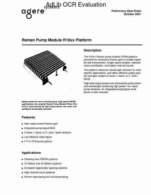
Ideally suited for use in ultralong-haul, high-speed DWDM applications, the versatile Raman Pump Module R18xx Platform is characterized by high output power, low noise, and multiband wavelength selection .
元器件交易网
a8e re
AdLib systems
OCR Evaluation
Preliminary Data Sheet October 2001
Raman Pump Module R18xx Platform
IXTT82N25P中文资料

Characteristic Values Min. Typ. Max. 250 2.5 5.0 ±100 25 250 35 V V nA µA µA mΩ
VGS = 10 V, ID = 0.5 ID25 Pulse test, t ≤ 300 µs, duty cycle d ≤ 2 %
PolarHTTM DMOS transistors utilize proprietary designs and process. US patent is pending.
90 80 70 VGS = 10V 9V 8V 2.6 2.4 2.2 VGS = 10V
V DS - Volts Fig. 4. RDS(on) Norm alized to ID25 Value vs. Junction Tem perature
ID - Amperes
60 50 40 30 20 10 0 0 1 2 3 5V 4 5 6 7 8 7V
Symbol Test Conditions (TJ = 25°C, unless otherwise specified) VDSS VGS(th) IGSS IDSS RDS(on) VGS = 0 V, ID = 250 µA VDS = VGS, ID = 250µA VGS = ±20 VDC, VDS = 0 VDS = VDSS VGS = 0 V TJ = 125°C
TO-264 (IXTK) Symbol VDSS VDGR VGSM ID25 ID(RMS) IDM IAR EAR EAS dv/dt PD TJ TJM Tstg TL Md Weight 1.6 mm (0.062 in.) from case for 10 s Mounting torque TO-3P TO-264 TO-268 TC = 25°C External lead current limit TC = 25°C, pulse width limited by TJM TC = 25°C TC = 25°C TC = 25°C IS ≤ IDM, di/dt ≤ 100 A/µs, VDD ≤ VDSS, TJ ≤ 150°C, RG = 4 Ω TC = 25°C Test Conditions TJ = 25°C to 150°C TJ = 25°C to 150°C; RGS = 1 MΩ Maximum Ratings 250 250 ±20 82 75 250 60 40 1.0 10 500 -55 ... +150 150 -55 ... +150 300 V V V A A A A mJ J V/ns W °C °C °C °C
IN4750A中文资料

For BZXyy series: Voltage rating 5.0 Third Line: Device name - For 1Nxx series: 7th to 8th characters of the device name.
or Large Die identification only for BZXyy series
XY
5th line: Date Code - Two Digit - Six Weeks Date Code
F
General Requirements:
1.0 Cathod Band
2.0 First Line: F - Fairchild Logo 3.0 Second Line: Device name - For 1Nxx series: 3rd to 4th characters of the device name.
Device
1N4748A 1N4749A 1N4750A 1N4751A 1N4752A
1N4753A 1N4754A 1N4755A 1N4756A 1N4757A
1N4758A 1N4759A 1N4760A 1N4761A 1N4762A
1N4763A 1N4764A
VZ (V) @ IZ (Note 1) Min. Typ. Max.
Value
1.0
6.67 -65 to +200
1SMB5956BT3G中文资料
550 mW
4.4 mW/°C 226 °C/W
Operating and Storage Temperature Range
TJ, Tstg −65 to °C +150
Stresses exceeding Maximum Ratings may damage the device. Maximum Ratings are stress ratings only. Functional operation above the Recommended Operating Conditions is not implied. Extended exposure to stresses above the Recommended Operating Conditions may affect device reliability. 1. FR−4 board, using recommended footprint.
Preferred devices are recommended choices for future use and best overall value.
Publication Order Number: 1SMB5913BT3/D
元器件交易网
1SMB5913BT3 Series
5.5
550
0.25
1
1SMB5927BT3, G 927B
11.4
12
12.6 31.2
6.5
550
0.25
1
1SMB5928BT3, G 928B 12.35 13 13.65 28.8
7
550
0.25
1
5.2
220
- 1、下载文档前请自行甄别文档内容的完整性,平台不提供额外的编辑、内容补充、找答案等附加服务。
- 2、"仅部分预览"的文档,不可在线预览部分如存在完整性等问题,可反馈申请退款(可完整预览的文档不适用该条件!)。
- 3、如文档侵犯您的权益,请联系客服反馈,我们会尽快为您处理(人工客服工作时间:9:00-18:30)。
Figure 6. Typ. Diode Capacitance vs. Reverse Voltage
Z thp – Thermal Resistance for Pulse Cond. (K/W)
1000
100 tp/T=0.5 tp/T=0.2 10 tp/T=0.1 tp/T=0.05 tp/T=0.02 1 10–4 tp/T=0.01
tp=10ms, half sinewave Tamb 65°C tp=20ms, half sinewave, Tj=175 °C I(BR)R=1A, Tj=175°C
x
40 –65...+175
Maximum Thermal Resistance
Tj = 25_C Parameter Junction ambient Test Conditions l=10mm, TL=constant on PC board with spacing 37.5mm Symbol RthJA RthJA Value 25 70 Unit K/W K/W
Peak forward surge current Repetitive peak forward current Average forward current Pulse avalanche peak power Pulse energy in avalanche mode, non repetitive (inductive load switch off) i2*t–rating Junction and storage temperature range
www.vishay.de • FaxBack +1-408-970-5600 2 (4)
Document Number 86051 Rev. 2, 24-Jun-98
元器件交易网
BYW82...BYW86
Vishay Telefunken
100 IF – Forward Current ( A ) Scattering Limit 10 CD – Diode Capacitance ( pF ) 3.0
Characteristics (Tj = 25_C unless otherwise specified)
R thJA – Therm. Resist. Junction / Ambient ( K/W ) 40 I FAV– Average Forward Current ( A ) 4
30
3
20 l 10 l
元器件交易网
BYW82...BYW86
Vishay Telefunken
Silicon Mesa Rectifiers
Features
D D D D D D
Glass passivated junction Hermetically sealed package Controlled avalanche characteristics Low reverse current High surge current loading Electrically equivalent diodes: BYW82 – 1N5624 BYW83 – 1N5625 BYW84 – 1N5626 BYW85 – 1N5627
94 9588
Applications
Rectifier, general purpose
Absolute Maximum Ratings
Tj = 25_C Parameter Reverse voltage g =Repetitive peak reverse voltage Test Conditions Type BYW82 BYW83 BYW84 BYW85 BYW86 Symbol VR=VRRM VR=VRRM VR=VRRM VR=VRRM VR=VRRM IFSM IFRM IFAV PR ER i2*t Tj=Tstg Value 200 400 600 800 1000 100 18 3 1000 20 Unit V V V V V A A A W mJ A2*s °C
2.0 1.6 1.2 0.8 0.4 0 0 40 80
I R – Reverse Current ( mA )
VR = VR RM f=1kHz RthJA=70K/W PCB
Scattering Limit 100
10
1 VR = VR RM 0 40 80 120 160 200
0.1 120 160 200
Document Number 86051 Rev. 2, 24-Jun-98
www.vishay.de • FaxBack +1-408-970-5600 1 (4)
元器件交易网
BYW82...BYW86
Vishay Telefunken Electrical Characteristics
94 9569
80 Tamb= 175°C
60
1 Tamb= 25°C
40
0.1
20
0.01 0
94 9567
0 0.6 1.2 1.8 2.4 0.1 1 10 100 VF – Forward Voltage ( V ) VR – Reverse Voltage ( V )
Figure 5. Max. Forward Current vs. Forward Voltage
Figure 1. Max. Thermal Resistance vs. Lead Length
Figure 3. Max. Average Forward Current vs. Ambient Temperature
1000
I FAV– Average Forward Current ( A )
Vishay Telefunken Ozone Depleting Substances Policy Statement
It is the policy of Vishay Semiconductor GmbH to 1. Meet all present and future national and international statutory requirements. 2. Regularly and continuously improve the performance of our products, processes, distribution and operating systems with respect to their impact on the health and safety of our employees and the public, as well as their impact on the environment. It is particular concern to control or eliminate releases of those substances into the atmosphere which are known as ozone depleting substances ( ODSs ). The Montreal Protocol ( 1987 ) and its London Amendments ( 1990 ) intend to severely restrict the use of ODSs and forbid their use within the next ten years. Various national and international initiatives are pressing for an earlier ban on these substances. Vishay Semiconductor GmbH has been able to use its policy of continuous improvements to eliminate the use of ODSs listed in the following documents. 1. Annex A, B and list of transitional substances of the Montreal Protocol and the London Amendments respectively 2 . Class I and II ozone depleting substances in the Clean Air Act Amendments of 1990 by the Environmental Protection Agency ( EPA ) in the USA 3. Council Decision 88/540/EEC and 91/690/EEC Annex A, B and C ( transitional substances ) respectively. Vishay Semiconductor GmbH can certify that our semiconductors are not manufactured with ozone depleting substances and do not contain such substances.
VR RM=1000V
RthJA=70K/W Tamb= 25°C
45°C 70°C 100°C 60°C
10–3
10–2
10–1
100
101
10–1
94 9568
tp – Pulse Length ( s )
101 IFRM rd Current ( A )
∅ 1.35 max.
26 min.
4.2 max.
26 min.
94 9587
Document Number 86051 Rev. 2, 24-Jun-98