BTA06-800TWRG中文资料
BTA06-600B中文资料

Absolute Maximum Ratings ( T J = 25°C unless otherwise specified )SymbolParameterCondition RatingsUnitsV DRM Repetitive Peak Off-State Voltage 600 V I T(RMS)R.M.S On-State Current T C = 94 °C6.0A I TSM Surge On-State Current One Cycle, 50Hz/60Hz, Peak, Non-Repetitive60/66A I 2t I 2t18A 2s PGM Peak Gate Power Dissipation 3.0W P G(AV)Average Gate Power Dissipation 0.3W I GM Peak Gate Current 2.0A V GM Peak Gate Voltage10V V ISO Isolation Breakdown Voltage(R.M.S.) A.C. 1 minute 1500V T J Operating Junction Temperature - 40 ~ 125°C T STGStorage Temperature - 40 ~ 150°C Mass2.0gMar, 2004. Rev. 0Features◆ Repetitive Peak Off-State Voltage : 600V ◆ R.M.S On-State Current ( I T(RMS)= 6 A )◆ High Commutation dv/dt◆ Isolation Voltage ( V ISO = 1500V AC )General DescriptionThis device is fully isolated package suitable for AC switchingapplication, phase control application such as fan speed and temperature modulation control, lighting control and static switching relay.This device is approved to comply with applicable require-ments by Underwriters Laboratories Inc.2.T23.Gate1.T1Symbol○○○▼▲1/6BTA06-600BSemiWell SemiconductorBi-Directional Triode Thyristorcopyright@SemiWell Semiconductor Co., Ltd., All rights reserved.UL : E228720PreliminaryElectrical CharacteristicsSymbol Items ConditionsRatingsUnit Min.Typ.Max.I DRM Repetitive Peak Off-StateCurrentV D = V DRM, Single Phase, Half WaveT J = 125 °C──1.0mAV TM Peak On-State Voltage I T = 8 A, Inst. Measurement── 1.5VI+GT1ⅠGate Trigger Current V D = 6 V, R L=10Ω──20mAI-GT1Ⅱ──20 I-GT3Ⅲ──20V+GT1ⅠGate Trigger Voltage V D = 6 V, R L=10Ω── 1.5VV-GT1Ⅱ── 1.5V-GT3Ⅲ── 1.5V GD Non-Trigger Gate Voltage T J = 125 °C, V D = 1/2 V DRM0.2──V(dv/dt)c Critical Rate of Rise Off-StateVoltage at CommutationT J = 125 °C, [di/dt]c = -3.0 A/ms,V D=2/3 V DRM5.0──V/㎲I H Holding Current─10─mAR th(j-c)Thermal Impedance Junction to case── 3.8°C/W BTA06-600B2/6Fig 4. On State Current vs.BTA06-600B4/6Fig 9. Gate Trigger Characteristics Test CircuitGGGTest Procedure ⅠTest Procedure ⅡTest Procedure ⅢBTA06-600BDim.mm Inch Min.Typ.Max.Min.Typ.Max.A 10.410.60.4090.417B 6.18 6.440.2430.254C 9.559.810.3760.386D 13.4713.730.5300.540E 6.05 6.150.2380.242F 1.26 1.360.0500.054G 3.17 3.430.1250.135H 1.87 2.130.0740.084I 2.57 2.830.1010.111J 2.540.100K 5.080.200L 2.51 2.620.0990.103M 1.25 1.550.0490.061N 0.450.630.0180.025O0.61.00.0240.039φ 3.70.146φ1 3.20.126φ21.50.059TO-220F Package Dimension5/6BTA06-600BDim.mm InchMin.Typ.Max.Min.Typ.Max.A10.410.60.4090.417B 6.18 6.440.2430.254C9.559.810.3760.386D8.48.660.3310.341E 6.05 6.150.2380.242F 1.26 1.360.0500.054G 3.17 3.430.1250.135H 1.87 2.130.0740.084I 2.57 2.830.1010.111J 2.540.100K 5.080.200L 2.51 2.620.0990.103M 1.25 1.550.0490.061N0.450.630.0180.025O0.6 1.00.0240.039P 5.00.197φ 3.70.146φ1 3.20.126φ2 1.50.059TO-220F Package Dimension, Forming6/6BTA06-600B。
BTA16中文资料_数据手册_参数
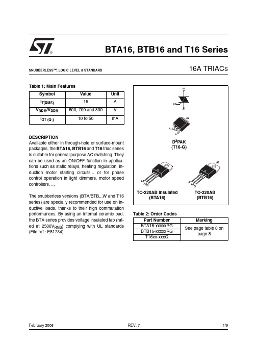
®1/9Table 1: Main FeaturesDESCRIPTIONAvailable either in through-hole or surface-mount packages, the BTA16, BTB16 and T16 triac series is suitable for general purpose AC switching. They can be used as an ON/OFF function in applica-tions such as static relays, heating regulation, in-duction motor starting circuits... or for phase control operation in light dimmers, motor speed controllers, ...The snubberless versions (BTA/BTB...W and T16series) are specially recommended for use on in-ductive loads, thanks to their high commutation performances. By using an internal ceramic pad,the BTA series provides voltage insulated tab (rat-ed at 2500V RMS ) complying with UL standards (File ref.: E81734).Symbol Value Unit I T(RMS)16A V DRM /V RRM 600, 700 and 800V I GT (Q 1)10 to 50mABTA16, BTB16 and T16 Series16A TRIAC SREV. 7February 2006SNUBBERLESS™, LOGIC LEVEL & STANDARDTable 2: Order CodesPart Number Marking BTA16-xxxxxRG See page table 8 onpage 8BTB16-xxxxxRG T16xx-xxxGBTA16, BTB16 and T16 Series2/9Table 3: Absolute Maximum Ratings Tables 4: Electrical Characteristics (T j = 25°C, unless otherwise specified)■SNUBBERLESS and Logic Level (3 quadrants)Symbol ParameterValue Unit I T(RMS)RMS on-state current (full sine wave)D 2PAK /TO-220AB T c = 100°C 16ATO-220AB Ins.T c = 15°C I TSM Non repetitive surge peak on-state current (full cycle, T j initial = 25°C) F = 50 Hz t = 20 ms 160A F = 60 Hz t = 16.7 ms168I ²t I ²t Value for fusingt p = 10 ms 144A ²s dI/dtCritical rate of rise of on-state cur-rent I G = 2 x I GT , t r ≤ 100 nsF = 120 HzT j = 125°C 50A/µs V DSM /V RSM Non repetitive surge peak off-state voltaget p = 10 msT j = 25°C V DSM /V RSM + 100V I GM Peak gate currentt p = 20 µsT j = 125°C 4A P G(AV)Average gate power dissipation T j = 125°C1W T stg T jStorage junction temperature range Operating junction temperature range- 40 to + 150- 40 to + 125°CSymbol Test ConditionsQuadrant T16BTA16 / BTB16Unit T1635SW CW BW I GT (1)V D = 12 V R L = 33 ΩI - II - III MAX.35103550mA V GT I - II - III MAX. 1.3V V GD V D = V DRM R L = 3.3 k ΩT j = 125°C I - II - IIIMIN.0.2V I H (2)I T = 500 mA MAX.35153550mA I L I G = 1.2 I GTI - III MAX.50255070mA II60306080dV/dt (2)V D = 67 %V DRM gate open T j = 125°C MIN.500405001000V/µs(dI/dt)c (2)(dV/dt)c = 0.1 V/µsT j = 125°C MIN.-8.5--A/ms(dV/dt)c = 10 V/µsT j = 125°C - 3.0--Without snubberT j = 125°C8.5-8.514BTA16, BTB16 and T16 Series3/9■Standard (4 quadrants)Table 5: Static Characteristics Table 6: Thermal resistance Symbol Test ConditionsQuadrant BTA16 / BTB16Unit C B I GT (1)V D = 12 V R L = 33 ΩI - II - III IV MAX.255050100mA V GT ALL MAX. 1.3V V GD V D = V DRM R L = 3.3 k Ω T j = 125°C ALLMIN.0.2V I H (2)I T = 500 mA MAX.2550mA I L I G = 1.2 I GTI - III - IVMAX.4060mA II 80120dV/dt (2)V D = 67 %V DRM gate openT j = 125°C MIN.200400V/µs (dV/dt)c (2)(dI/dt)c = 7 A/ms T j = 125°CMIN.510V/µsSymbol Test ConditionsValue Unit V T (2)I TM = 22.5 A t p = 380 µs T j = 25°C MAX. 1.55V V to (2)Threshold voltage T j = 125°C MAX.0.85V R d (2)Dynamic resistance T j = 125°C MAX.25m ΩI DRM I RRMV DRM = V RRMT j = 25°C MAX.5µA T j = 125°C2mANote 1: minimum I GT is guaranted at 5% of I GT max.Note 2: for both polarities of A2 referenced to A1.Symbol ParameterValue Unit R th(j-c)Junction to case (AC)D 2PAK / TO-220AB 1.2°C/WTO-220AB Insulated 2.1R th(j-a)Junction to ambient S = 1 cm ²D 2PAK45°C/WTO-220AB / TO-220AB Insulated60S = Copper surface under tab.BTA16, BTB16 and T16 Series4/9Figure 1: Maximum power dissipation versus RMS on-state current (full cycle)Figure 2: RMS on-state current versus case temperature (full cycle)Figure 3: RMS on-state current versus ambient temperature (printed circuit board FR4, copper thickness: 35µm) (full cycle)Figure 4: Relative variation of thermal impedance versus pulse durationFigure 5: On-state characteristics (maximum values)Figure 6: Surge peak on-state current versus number of cyclesBTA16, BTB16 and T16 Series5/9Figure 7: Non-repetitive surge peak on-state current for a sinusoidal pulse with width t p < 10 ms and corresponding value of I 2tFigure 8: Relative variation of gate trigger current, holding current and latching current versus junction temperature (typical values)Figure 9: Relative variation of critical rate of decrease of main current versus (dV/dt)c (typical values) (Snubberless & L ogic level types)Figure 10: Relative variation of critical rate of decrease of main current versus (dV/dt)c (typical values) (Standard types)Figure 11: D 2P AK Thermal resistance junction to ambient versus copper surface under tab (printed circuit board FR4, copper thickness: 35µm)BTA16, BTB16 and T16 Series6/9Figure 12: Ordering Information Scheme (BTA16 and BTB16 series)Figure 13: Ordering Information Scheme (T16 series)Table 7: Product SelectorPart Numbers Voltage (xxx)Sensitivity Type Package 600 V 700 V 800 V BTA/BTB16-xxxB X X X 50 mA Standard TO-220AB BTA/BTB16-xxxBW X X X 50 mA Snubberless TO-220AB BTA/BTB16-xxxCX X X 25 mA Standard TO-220AB BTA/BTB16-xxxCW X X X 35 mA Snubberless TO-220AB BTA/BTB16-xxxSW X XX 10 mA Logic level TO-220ABT1635-xxxGXX35 mASnubberlessD 2PAKBTB: non insulated TO-220AB packageBTA16, BTB16 and T16 Series Figure 14: D2PAK Package Mechanical DataFigure 15: D2PAK Foot Print Dimensions(in millimeters)7/9BTA16, BTB16 and T16 Series8/9In order to meet environmental requirements, ST offers these devices in ECOPACK® packages. These packages have a Lead-free second level interconnect . The category of second level interconnect is marked on the package and on the inner box label, in compliance with JEDEC Standard JESD97. The maximum ratings related to soldering conditions are also marked on the inner box label. ECOPACK is an ST trademark. ECOPACK specifications are available at: .Table 8: Ordering InformationOrdering type Marking Package Weight Base qtyDelivery modeBTA/BTB16-xxxyzRGBTA/BTB16xxxyz TO-220AB 2.3 g 50Tube T1635-xxxG T1635xxxG D 2PAK1.5 g50Tube T1635-xxxG-TRT1635xxxG1000Tape & reelNote: xxx = voltage, yy = sensitivity, z = typeTable 9: Revision HistoryDate Revision Description of ChangesOct-20026A Last update.13-Feb-20067TO-220AB delivery mode changed from bulk to tube.ECOPACK statement added.BTA16, BTB16 and T16 Series Information furnished is believed to be accurate and reliable. However, STMicroelectronics assumes no responsibility for the consequencesof use of such information nor for any infringement of patents or other rights of third parties which may result from its use. No license is granted by implication or otherwise under any patent or patent rights of STMicroelectronics. Specifications mentioned in this publication are subject to change without notice. This publication supersedes and replaces all information previously supplied. STMicroelectronics products are notauthorized for use as critical components in life support devices or systems without express written approval of STMicroelectronics.The ST logo is a registered trademark of STMicroelectronics.All other names are the property of their respective owners© 2006 STMicroelectronics - All rights reservedSTMicroelectronics group of companiesAustralia - Belgium - Brazil - Canada - China - Czech Republic - Finland - France - Germany - Hong Kong - India - Israel - Italy - Japan - Malaysia - Malta - Morocco - Singapore - Spain - Sweden - Switzerland - United Kingdom - United States of America9/9万联芯城-电子元器件采购网,提供一站式配套,解决物料烦恼,万联芯城是国内优质的电子元器件供应商,货源渠道来自原厂及代理商,只售原装现货,只需提交BOM物料清单,我们将为您报出一个满意的价格,解决客户采购烦恼,为客户节省采购成本,点击进入万联芯城。
BT系巨型望远镜用户手册说明书

BT SeriesGiant BinocularsBT-70SF - BT-82SF - BT-100SF - BT-120SF Art. No. 0114200 / 0114210 / 0114220 / 0114230U-Mount with tripodArt. No. 0114300 INSTRUCTION MANUALGiant binoculars2x 62° LER eyepiece20mm ArTripodwith spacing plate and central screwU-Mountwith mounting plateand tripod head adapterTripodU-Mount11. F riction wheelsfor height adjustment 12. Movable height cradle 13. Fork arm14. Adapter plate for 15.15. 1/4" threaded screws 16. Dovetail rail 17. F ixing screws for 16.18. Turnable azimuthal axis 19. Fixing screw for 18.20. Mounting head21. Tripod head adapter1. Tripod head2. Tripod leg (upper part)3. Fixing screws for tripod leg4. Tripod leg (lower part)5. Spindle crank6. K nurled screw7. Central screw8. Spacing plate9. Washer 10. C-Clip21. Objective Lens 22. Dew/sun protection cap, extendable 23. Tube24. ¼" Connection thread 25. ⅜"-Connection thread* with unscrewable¼“ Connection thread adapter26. Transport handle27. Eyepiece, exchangeable 28. Eyepiece holder29. Eyepiece clamping ring 30. Focusing31. Interpupillary distance adjustmentGiant binoculars * for mounting on photo tripods with corresponding mounting head. ¼" connection thread can be unscrewed using a slotted screwdriver, thus exposing a "⅜"connection thread.When mounting the binoculars on a photo tripod with appropriate mounting head, make sure that the photo tripod and the mountinghead have sufficient load-bearing capacity!plate in the tripod head and fix it.adapter and the tripod. Tighten the tripod legs with the knurled screw.2. A ssemble spacing plate and central screw.6. F riction adjustment of the coupling for the height axis.them.tripod head. Place the U-Mount on the tripod head adapter.7. F riction adjustment of the coupling for the azimuth axis.bottom side of the binoculars.handle and tighten the fixing screws.guide of the U-Mount.12. B alance the binoculars at the centreof gravity.8. 2 x ¼" connection thread on the bottom side of the binocularsobservation. Possibly pull out theeyepiece holder.focusing.14. R emove the dust caps from theobjective lenses.Astronomical observations48Land observations48Tips on observationMoon*Star cluster M45 Pleiades*Orion nebula M42*Landscape*Birds*Ships** Sample images for illustration purposes. The actual image size and image quality depends on the selected eyepieces. Astronomical motifs are usually not visible in colour due to the long observation distance.EXPLORE SCIENTIFIC Eyepiece series EXPLORE SCIENTIFIC TELRADProjection viewfinder with baseEXPLORE SCIENTIFIC Nebula filters EXPLORE SCIENTIFIC Filter Set 2When using optional accessories, read separate instruction manual!Only use accessories authorized by the manufacturer!11Giant binoculars Product (Art. No.)Objective lens typeAperture (mm)Focal length (mm)Dimensions(LxWxH) (mm)Weight (kg)BT-70SF (0114200)achromatic (2 elem./1 gr.)70400370x213x122 3.4BT-82SF (0114210)achromatic (2 elem./1 gr.)82470445x226x122 4.3BT-100SF (0114220)achromatic (2 elem./1 gr.)100550520x270x155 6.8BT-120SF (0114230)achromatic (2 elem./1 gr.)120660654x290x1568.3Giant binoculars• C lean the lenses (eyepieces and/or objective lenses) only with a soft and lint-free cloth (e.g. microfibre cloth). To avoid scratching the lenses, use only gentle pressure with the cleaning cloth.• T o remove more stubborn dirt, moisten the cleaning cloth with an eyeglass-cleaning solution and wipe the lenses gently.• P rotect the device from dust and moisture! After use, particularly in high humidity, let the device acclimatise at room temperature for a short period of time, so that the residual moisture can dissipate. Put the dust caps on and store it in a dry and heated place.U-Mount and tripod• Clean the device only on the outside with a dry cloth.Bresser GmbHGutenbergstr. 2 · DE-46414 RhedeGermanywww.bresser.de·******************Errors and technical changes excepted.Manual_0114200-0114210-0114220-0114230-0114300_BT-Series-U-Mount_en_EXPSC_062021a。
BTA60-800B

符号 单位
VDRMM
V
IH
mA
IGT
mA
VGT
V
规范值
Min
Max
800
1000
50
1.1
1.3
50
≤50 ≤50 ≤50 ≤1.3 ≤1.3 ≤1.3
测试条件
ID=0.1mA VDRM=520v
IT=32A IT=0.2A,IGT=50mA VAK=12V,RL=10Ω
VD=12V,RL=10Ω
深圳市品电科技有限公司
Shenzhen piandian Technology Co.,ltd
60A双向可控硅 ● 型号:BTA60-800B ● 封装:特殊封装 ● 用途:主要用于变频电路,电动工具开关、调温、调速电 路、洗衣机、微波炉、空调等家用电器的控制电路。
极限参数(Ta=25℃)
参数名称 断态重复峰值电压 反向重复峰值电压
通态平均电流 通态不重复浪涌电流
结温 贮存温度
符号 额定值 单位
VDRM
>800
V
VRRM
>800
V
IT
60
A
ITSM
600
A
TJ
-40~125
℃
Tatg -40~150
℃
电参数(Ta=25℃)
参数名称
断态重复峰值电压
断态重复峰值电流
通态峰值电压
维持电流
控制极触发电 流
控制极触发电 压
T2+G+ T2+GT2-GT2+G+ T2+GT2-G-
Tel:0755-23029786、15914021719 PDKJ ELECTRONICS CO., LTD.
CBW系列大电流贴片磁珠规格书
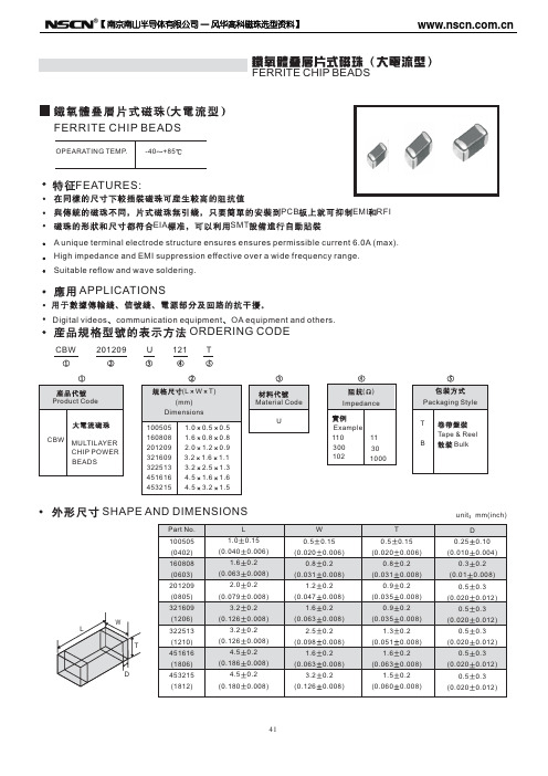
FERRITE CHIP BEADS
FERRITE CHIP BEADS
OPEARATING TEMP. -40 +85
FEATURES:
PCB EIA SMT EMI RFI
A unique terminal electrode structure ensures ensures permissible current 6.0A (max). High impedance and EMI suppression effective over a wide frequency range. Suitable reflow and wave soldering.
2012 TYPE
Part No. CBW201209U050 CBW201209U110 CBW201209U260 CBW201209U310 CBW201209U500 CBW201209U600 CBW201209U800 CBW201209U121 CBW201209U151 CBW201209U181 CBW201209U221 CBW201209U301 CBW201209U501 CBW201209U601 CBW201209U801 CBW201209U102 CBW201209U122 CBW201209U202 Impedance( At 100MHz 0~15 7~15 26 31 50 60 80 120 150 180 220 300 500 600 800 1000 1200 2000 25% 25% 25% 25% 25% 25% 25% 25% 25% 25% 25% 25% 25% 25% 25% 25% ) DCR ( )Max Ir (A)Max 3 3 3 3 3 3 2.5 2 2 2 2 2 1.5 1.5 0.8 0.8 0.5 0.3
美国艾顿公司滤芯技术产品说明说明书

10
10
Refinery Overview and Application Portfolio
11
11
Refinery Flow Diagram
H2
Sour Gas
Amine Treating
Fuel Gas H2S
Claus Reactor
Sulfur
Gas
Gas Processing
Merox Treater
This is a photographic template – your photograph should fit precisely within this rectangle.
Filtration Technology for Oil & Gas
EATON FILTRATION (JAPAN) Ltd. Sales Manager. Shuji Yamaguchi.
world
4
4
Eaton’s growth through acquisitions
Ronningen-Petter (Sep. 2006)
• Application focused engineering in a range of industrial markets
• Range of unique solid-liquid separation and self-cleaning products
9
Markets & Industries Served
Marine
• Gearboxes • Shipbuilding Industry • Tankers
Refrigeration
Machines
BTA201-800ER中文资料

K/W
102 Zth(j-lead)
(K/W) 10
1
001aag962
(1) (2)
10−1
10−2
10−5
10−4
10−3
10−2
10−1
1
(1) Unidirectional (2) Bidirectional Fig 6. Transient thermal impedance from junction to lead as a function of pulse width
BTA201-600E
BTA201-800B
BTA201-800E
BTA201-800ER
4. Limiting values
Version SOT54
Table 3. Limiting values In accordance with the Absolute Maximum Rating System (IEC 60134).
Passivated, guaranteed commutation triacs in a plastic package. The ‘sensitive gate’ E and ER series are intended for interfacing with low power drivers, including microcontrollers. The high commutation B series are designed to commutate the full RMS current at the maximum junction temperature without the aid of a snubber.
5. Thermal characteristics
BTA16-600BW3G;BTA16-800BW3G;中文规格书,Datasheet资料

TJ
−40 to +125 °C
Storage Temperature Range
Tstg −40 to +150 °C
RMS Isolation Voltage (t = 300 ms, R.H. ≤ 30%, TA = 25°C)
Viso
2500
V
Stresses exceeding Maximum Ratings may damage the device. Maximum Ratings are stress ratings only. Functional operation above the Recommended Operating Conditions is not implied. Extended exposure to stresses above the Recommended Operating Conditions may affect device reliability. 1. VDRM and VRRM for all types can be applied on a continuous basis. Blocking
/
3
TC, CASE TEMPERATURE (°C)
− MT2 NEGATIVE (Negative Half Cycle)
All polarities are referenced to MT1. With in−phase signals (using standard AC lines) quadrants I and III are used.
+
(+) MT2
(+) MT2
Quadrant II IGT −
- 1、下载文档前请自行甄别文档内容的完整性,平台不提供额外的编辑、内容补充、找答案等附加服务。
- 2、"仅部分预览"的文档,不可在线预览部分如存在完整性等问题,可反馈申请退款(可完整预览的文档不适用该条件!)。
- 3、如文档侵犯您的权益,请联系客服反馈,我们会尽快为您处理(人工客服工作时间:9:00-18:30)。
1/6®BTA/BTB06 SeriesSNUBBERLESS ™, LOGIC LEVEL & STANDARD6A TRIAC SApril 2002 - Ed: 5AMAIN FEATURES:DESCRIPTIONSuitable for AC switching operations, the BTA/BTB06 series can be used as an ON/OFF function in applications such as static relays, heating regulation, induction motor starting circuits... or for phase control in light dimmers, motor speed controllers,...The snubberless and logic level versions (BTA/BTB...W) are specially recommended for use on inductive loads, thanks to their high commutation performances. By using an internal ceramic pad,the BTA series provides voltage insulated tab (rated at 2500V RMS) complying with UL standards (File ref.: E81734)Symbol Value Unit I T(RMS)6A V DRM /V RRM600 and 800VI G (Q 1)5 to 50mAABSOLUTE MAXIMUM RATINGSSymbol ParameterValueUnit I T(RMS)RMS on-state current (full sine wave)TO-220ABTc = 110°C 6ATO-220AB Ins.Tc = 105°C I TSM Non repetitive surge peak on-state current (full cycle, Tj initial = 25°C) F = 50 Hz t = 20 ms 60AF = 60 Hzt = 16.7 ms63I ²t I ²t Value for fusingtp = 10 ms21A ²s dI/dt Critical rate of rise of on-state current I G = 2 x I GT , tr ≤ 100 ns F = 120 Hz Tj = 125°C 50A/µs I GM Peak gate currenttp = 20 µsTj = 125°C 4A P G(AV)Average gate power dissipation Tj = 125°C1W T stg T jStorage junction temperature range Operating junction temperature range- 40 to + 150- 40 to + 125°CBTA/BTB06 Series2/6ELECTRICAL CHARACTERISTICS (Tj = 25°C, unless otherwise specified)sSNUBBERLESS™ and LOGIC LEVEL (3 Quadrants)sSTANDARD (4 Quadrants)STATIC CHARACTERISTICSNote 1: minimum IGT is guaranted at 5% of IGT max.Note 2: for both polarities of A2 referenced to A1Symbol Test ConditionsQuadrantBTA/BTB06UnitTWSW CW BW I GT (1)V D = 12 V R L = 30 ΩI - II - III MAX.5103550mA V GT I - II - III MAX. 1.3V V GD V D = V DRM R L = 3.3 k ΩTj = 125°C I - II - IIIMIN.0.2V I H (2)I T = 100 mA MAX.10153550mA I L I G = 1.2 I GTI - III MAX.10255070mA II15306080dV/dt (2)V D = 67 %V DRM gate open Tj = 125°CMIN.20404001000V/µs (dI/dt)c (2)(dV/dt)c = 0.1 V/µs Tj = 125°C MIN.2.73.5--A/ms(dV/dt)c = 10 V/µs Tj = 125°C 1.2 2.4--Without snubber Tj = 125°C-- 3.55.3Symbol Test ConditionsQuadrant BTA/BTB06UnitCB I G (1)V D = 12 V R L = 30 ΩI - II - III IV MAX.255050100mA V GT ALL MAX. 1.3V V GD V D = V DRM R L = 3.3 k Ω Tj = 125°C ALLMIN.0.2V I H (2)I T = 500 mA MAX.2550mA I L I G = 1.2 I GTI - III - IVMAX.4050mA II80100dV/dt (2)V D = 67 %V DRM gate open Tj = 125°CMIN.200400V/µs (dV/dt)c (2)(dI/dt)c = 2.7 A/ms Tj = 125°CMIN.510V/µsSymbol Test ConditionsValue Unit V T (2)I TM = 5.5 A tp = 380 µs Tj = 25°C MAX. 1.55V V to (2)Threshold voltage Tj = 125°C MAX.0.85V R d (2)Dynamic resistance Tj = 125°C MAX.60m ΩI DRM I RRMV DRM = V RRMTj = 25°C MAX.5µA Tj = 125°C1mABTA/BTB06 Series3/6THERMAL RESISTANCESPRODUCT SELECTORBTB: non insulated TO-220AB packageORDERING INFORMATIONOTHER INFORMATIONNote: xxx = voltage, y = sensitivity, z = typeSymbol ParameterValue Unit R th(j-c)Junction to case (AC)TO-220AB 1.8°C/WTO-220AB Insulated 2.7R th(j-a)Junction to ambientTO-220ABTO-220AB Insulated60°C/W Part NumberVoltage (xxx)SensitivityType Package 600 V800 V BTA/BTB06-xxxB X X 50 mA Standard TO-220AB BTA/BTB06-xxxBW X X 50 mA Snubberless TO-220AB BTA/BTB06-xxxC X X 25 mA Standard TO-220AB BTA/BTB06-xxxCW X X 35 mA Snubberless TO-220AB BTA/BTB06-xxxSW X X 10 mA Logic level TO-220AB BTA/BTB06-xxxTWXX5 mALogic levelTO-220ABPart NumberMarkingWeight Base quantity Packing mode BTA/BTB06-xxxyz BTA/BTB06-xxxyz 2.3 g 250Bulk BTA/BTB06-xxxyzRGBTA/BTB06-xxxyz2.3 g50TubeBTA/BTB06 Series4/6Fig. 1: Maximum power dissipation versus RMS on-state current (full cycle).Fig. 2: RMS on-state current versus case temperature (full cycle).Fig. 3: Relative variation of thermal impedance versus pulse duration.Fig. 4: On-state characteristics (maximum values).Fig. 5: Surge peak on-state current versus number of cycles.Fig. 6: Non-repetitive surge peak on-state current for a sinusoidal pulse with width tp <10ms, and corresponding value of I²t.BTA/BTB06 Series5/6Fig. 7: Relative variation of gate trigger current,holding current and latching current versus junction temperature (typical values).Fig. 8-1: Relative variation of critical rate of decrease of main current versus (dV/dt)c (typical values). Snubberless & Logic Level T ypesFig. 8-2: Relative variation of critical rate of decrease of main current versus (dV/dt)c (typical values). Standard T ypesFig. 9: Relative variation of critical rate of decrease of main current versus junction temperature.BTA/BTB06 SeriesPACKAGE MECHANICAL DATAInformation furnished is believed to be accurate and reliable. However, STMicroelectronics assumes no responsibility for the consequences of use of such information nor for any infringement of patents or other rights of third parties which may result from its use. No license is granted by implication or otherwise under any patent or patent rights of STMicroelectronics. Specifications mentioned in this publication are subject to change without notice. This publication supersedes and replaces all information previously supplied. STMicroelectronics products are not authorized for use as critical components in life support devices or systems without express written approval of STMicroelectronics.© The ST logo is a registered trademark of STMicroelectronics© 2002 STMicroelectronics - Printed in Italy - All Rights ReservedSTMicroelectronics GROUP OF COMPANIESAustralia - Brazil - Canada - China - Finland - France - GermanyHong Kong - India - Isreal - Italy - Japan - Malaysia - Malta - Morocco - SingaporeSpain - Sweden - Switzerland - United Kingdom - United States.6/6。