5550EX103Z5中文资料
SINDOH圣度-机皇MF5550H(spruce)高速一体机介绍

便利的操作面板
9英寸大型彩色触摸屏,所有功能一览无余 在画面登录经常使用的功能,使用便捷 各个功能用窗口表示,可以根据自己的喜好进行变更
9英寸大型触摸屏
9英寸 大型彩色触摸屏,使用方便
5/95
3. 详细特征
画质改善
采用CTI Toner ,实现 Real 1,200 dpi 高品质画像打印
23/95
Ⅰ. 交货安装
Ⅱ. 外形 及 附件 Ⅲ. PPC主要功能
Ⅴ. SCAN主要功能
Ⅵ. 传真主要功能
Ⅶ. 保养
Ⅳ. PRINT主要功能
24/95
AD9910BSVZ资料

1 GSPS, 14-Bit, 3.3 V CMOSDirect Digital SynthesizerAD9910 Rev. 0Information furnished by Analog Devices is believed to be accurate and reliable. However, noresponsibility is assumed by Analog Devices for its use, nor for any infringements of patents or other rights of third parties that may result from its use. Specifications subject to change without notice. No license is granted by implication or otherwise under any patent or patent rights of Analog Devices. T rademarks and registered trademarks are the property of their respective owners. One Technology Way, P.O. Box 9106, Norwood, MA 02062-9106, U.S.A. Tel: 781.329.4700 Fax: 781.461.3113 ©2007 Analog Devices, Inc. All rights reserved.FEATURES1 GSPS internal clock speed (up to 400 MHz analog output) Integrated 1 GSPS, 14-bit DAC32-bit tuning wordPhase noise ≤ −125 dBc/Hz @ 1 kHz offset (400 MHz carrier) Excellent dynamic performance with>80 dB narrow-band SFDRSerial input/output (I/O) controlAutomatic linear or arbitrary frequency, phase, and amplitude sweep capability8 frequency and phase offset profiles1.8 V and 3.3 V power suppliesSoftware and hardware controlled power-down100-lead TQFP_EP packageIntegrated 1024 word × 32-bit RAMPLL REFCLK multiplierParallel datapath interfaceInternal oscillator, can be driven by a single crystalPhase modulation capabilityAmplitude modulation capabilityMultichip synchronization APPLICATIONSAgile local oscillator (LO) frequency synthesis Programmable clock generatorFM chirp source for radar and scanning systems Test and measurement equipmentAcousto-optic device driversPolar modulatorFast frequency hoppingFUNCTIONAL BLOCK DIAGRAMFigure 1.AD9910Rev. 0 | Page 2 of 60TABLE OF CONTENTSFeatures..............................................................................................1 Applications.......................................................................................1 Functional Block Diagram..............................................................1 Revision History...............................................................................3 General Description.........................................................................4 Specifications.....................................................................................5 Electrical Specifications...............................................................5 Absolute Maximum Ratings............................................................8 Equivalent Circuits.......................................................................8 ESD Caution..................................................................................8 Pin Configuration and Function Descriptions.............................9 Typical Performance Characteristics...........................................12 Application Circuits.......................................................................15 Theory of Operation......................................................................16 Single Tone Mode.......................................................................16 RAM Modulation Mode............................................................17 Digital Ramp Modulation Mode..............................................18 Parallel Data Port Modulation Mode.......................................19 Parallel Data Clock (PDCLK)...............................................19 Transmit Enable (TxENABLE).............................................20 Mode Priority..............................................................................21 Functional Block Detail.................................................................22 DDS Core.....................................................................................22 14-Bit DAC Output....................................................................22 Auxiliary DAC........................................................................23 Inverse Sinc Filter.......................................................................23 Clock Input (REF_CLK)............................................................23 REF_CLK Overview..............................................................23 Crystal Driven REF_CLK.....................................................24 Direct Driven REF_CLK.......................................................24 Phase-Locked Loop (PLL) Multiplier..................................24 PLL Charge Pump (25)External PLL Loop Filter Components...............................25 PLL Lock Indication..................................................................26 Output Shift Keying (OSK).......................................................26 Manual OSK............................................................................26 Automatic OSK.......................................................................26 Digital Ramp Generator (DRG)...............................................27 DRG Overview.......................................................................27 DRG Slope Control................................................................29 DRG Limit Control................................................................29 DRG Accumulator Clear.......................................................29 Normal Ramp Generation....................................................29 No-Dwell Ramp Generation.................................................31 DROVER Pin..........................................................................31 RAM Control..............................................................................32 RAM Overview.......................................................................32 Load/Retrieve RAM Operation............................................32 RAM Playback Operation (Waveform Generation)..........32 RAM_SWP_OVR (RAM Sweep Over) Pin........................33 Overview of RAM Playback Modes....................................33 RAM Direct Switch Mode.....................................................33 RAM Direct Switch Mode with Zero-Crossing.................34 RAM Ramp Up Mode...........................................................34 RAM Ramp Up Internal Profile Control Mode.................34 Internal Profile Control Continuous Waveform Timing Diagram...................................................................................37 RAM Bidirectional Ramp Mode..........................................37 RAM Continuous Bidirectional Ramp Mode....................38 RAM Continuous Recirculate Mode...................................40 Additional Features........................................................................41 Profiles.........................................................................................41 I/O_Update Pin..........................................................................41 Automatic I/O Update (41)AD9910Rev. 0 | Page 3 of 60Power-Down Control (41)Synchronization of Multiple Devices............................................43 Serial Programming........................................................................46 Control Interface—Serial I/O....................................................46 General Serial I/O Operation....................................................46 Instruction Byte...........................................................................46 Instruction Byte Information Bit Map.................................46 Serial I/O Port Pin Descriptions...............................................46 SCLK—Serial Clock................................................................46 CS —Chip Select Bar...............................................................46 SDIO—Serial Data Input/Output.........................................46 SDO—Serial Data Out...........................................................46 I/O_RESET—Input/Output Reset........................................46 I/O_UPDATE—Input/Output Update................................47 Serial I/O Timing Diagrams......................................................47 MSB/LSB Transfers.....................................................................47 Register Map and Bit Descriptions...............................................48 Register Bit Descriptions............................................................53 Control Function Register 1 (CFR1)....................................53 Control Function Register 2 (CFR2)....................................55 Control Function Register 3 (CFR3)....................................56 Auxiliary DAC Control Register...........................................56 I/O Update Rate Register.......................................................57 Frequency Tuning Word Register (FTW)...........................57 Phase Offset Word Register (POW).....................................57 Amplitude Scale Factor Register (ASF)...............................57 Multichip Sync Register.........................................................58 Digital Ramp Limit Register..................................................58 Digital Ramp Step Size Register............................................58 Digital Ramp Rate Register...................................................58 Profile Registers......................................................................59 Outline Dimensions........................................................................60 Ordering Guide (60)REVISION HISTORY5/07—Revision 0: Initial VersionAD9910Rev. 0 | Page 4 of 60GENERAL DESCRIPTIONThe AD9910 is a direct digital synthesizer (DDS) featuring an integrated 14-bit DAC and supporting sample rates up to 1 GSPS. The AD9910 employs an advanced, proprietary DDS technology that provides a significant reduction in power con-sumption without sacrificing performance. The DDS/DAC combination forms a digitally programmable, high frequency, analog output synthesizer capable of generating a frequency agile sinusoidal waveform at frequencies up to 400 MHz. The user has access to the three signal control parameters that control the DDS: frequency, phase, and amplitude. The DDS provides fast frequency hopping and frequency tuning resolu-tion with its 32-bit accumulator. With a 1 GSPS sample rate, the tuning resolution is ~0.23 Hz. The DDS also enables fast phase and amplitude switching capability.The AD9910 is controlled by programming its internal control registers via a serial I/O port. The AD9910 includes an integrated static RAM to support various combinations of frequency, phase, and/or amplitude modulation. The AD9910 also supports a user defined, digitally controlled, digital ramp mode of operation. In this mode, the frequency, phase, or amplitude can be varied linearly over time. For more advanced modulation functions, a high speed parallel data input port is included to enable direct frequency, phase, amplitude, or polar modulation.The AD9910 is specified to operate over the extended industrial temperature range (see the Absolute Maximum Ratings section for details).06479-002PARALLELINPUTPDCLKSCLK SDIO I/O_RESETPROFILE I/O_UPDATEE X T _P W R _D W NCS TxENABLEOSK DRCTL DRHOLD DROVER S Y N C _S M P _E R RS Y N C _C L KS Y N C _O U TS Y N C _I NP L L _L O C KP L L _L O O P _F I L T E RM A S T E R _R E S E TFigure 2. Detailed Block DiagramAD9910Rev. 0 | Page 5 of 60SPECIFICATIONSELECTRICAL SPECIFICATIONSAVDD (1.8 V) and DVDD (1.8 V) = 1.8 V ± 5%, AVDD (3.3 V) = 3.3 V ± 5%, DVDD_I/O = 3.3 V ± 5%, T = 25°C, R SET = 10 kΩ, I OUT = 20 mA, external reference clock frequency = 1000 MHz with REFCLK multiplier disabled, unless otherwise noted. Table 1.Parameter Conditions/Comments Min Typ Max Unit REF_CLK INPUT CHARACTERISTICS Frequency Range REFCLK Multiplier Disabled 25 1000 MHz Enabled 3.2 60 MHz Maximum REFCLK Input Divider Frequency Full temperature range 1500 1900 MHz Minimum REFCLK Input Divider Frequency Full temperature range 25 35 MHz External Crystal 25 MHz Input Capacitance 3 pF Input Impedance Differential 2.8 kΩ Single-ended 1.4 kΩ Duty Cycle REFCLK multiplier disabled 45 55 % REFCLK multiplier enabled 40 60 % REF_CLK Input level Single-ended 50 1000 mV p-p Differential 100 2000 mV p-p REFCLK MULTIPLIER VCO CHARACTERISTICS VCO Gain (K V ) @ Center Frequency VCO range Setting 0 429 MHz/V VCO range Setting 1 500 MHz/V VCO range Setting 2 555 MHz/V VCO range Setting 3 750 MHz/V VCO range Setting 4 789 MHz/VVCO range Setting 51850 MHz/V REFCLK_OUT CHARACTERISTICS Maximum Capacitive Load 20 pF Maximum Frequency 25 MHz DAC OUTPUT CHARACTERISTICS Full-Scale Output Current 8.6 20 31.6 mA Gain Error −10 +10 %FS Output Offset 2.3 μA Differential Nonlinearity 0.8 LSB Integral Nonlinearity 1.5 LSB Output Capacitance 5 pF Residual Phase Noise @ 1 kHz offset, 20 MHz A OUT REFCLK Multiplier Disabled −152 dBc/Hz Enabled @ 20× −140 dBc/Hz Enabled @ 100× −140 dBc/Hz Voltage Compliance Range −0.5 +0.5 V Wideband SFDR See the Typical PerformanceCharacteristics sectionNarrow-Band SFDR 50.1 MHz Analog Output ±500 kHz –87 dBc ±125 kHz –87 dBc ±12.5 kHz –96 dBc 101.3 MHz Analog Output ±500 kHz –87 dBc ±125 kHz –87 dBc ±12.5 kHz –95 dBcAD9910Rev. 0 | Page 6 of 60Parameter Conditions/Comments Min Typ Max Unit201.1 MHz Analog Output ±500 kHz –87 dBc ±125 kHz –87 dBc ±12.5 kHz –91 dBc 301.1 MHz Analog Output ±500 kHz –86 dBc ±125 kHz –86 dBc ±12.5 kHz –88 dBc 401.3 MHz Analog Output ±500 kHz –84 dBc ±125 kHz –84 dBc ±12.5 kHz –85 dBc SERIAL PORT TIMING CHARACTERISTICS Maximum SCLK Frequency 70 Mbps Minimum SCLK Clock Pulse Width Low 4 ns High 4 ns Maximum SCLK Rise/Fall Time 2 ns Minimum Data Setup Time to SCLK 5 ns Minimum Data Hold Time to SCLK 0 ns Maximum Data Valid Time in Read Mode 11 nsI/O_UPDATE/PS0/PS1/PS2 TIMINGCHARACTERISTICSMinimum Pulse Width High 1 SYNC_CLK cycle Minimum Setup Time to SYNC_CLK 2 ns Minimum Hold Time to SYNC_CLK 0 nsTx_ENABLE and 16-BIT PARALLEL (DATA) BUSTIMINGMaximum PDCLK Frequency 250 MHz Tx_ENABLE/Data Setup Time (to PDCLK) 2 ns Tx_ENABLE/Data Hold Time (to PDCLK) 1 ns MISCELLANEOUS TIMING CHARACTERISTICS Wake-Up Time 2 1 ms Fast Recovery 8 SYSCLK cycles Full Sleep Mode 150 μs Minimum Reset Pulse Width High 5 SYSCLK cycles 3DATA LATENCY (PIPE_LINE DELAY) Data Latency, Single Tone or using Profiles Frequency, Phase, Amplitude-to-DAC Output Matched latency enabled and OSKenabled91 SYSCLK cycles Frequency, Phase-to-DAC Output Matched latency enabled and OSKdisabled79 SYSCLK cycles Matched latency disabled 79 SYSCLK cycles Amplitude-to-DAC Output Matched latency disabled 47 SYSCLK cycles Data Latency using RAM Mode Frequency, Phase-to-DAC Output Matched latency enabled/disabled 94 SYSCLK cycles Amplitude-to-DAC Output Matched latency enabled 106 SYSCLK cycles Matched latency disabled 58 SYSCLK cycles Data Latency, Sweep Mode Frequency, Phase-to-DAC Output Matched latency enabled/disabled 91 SYSCLK cycles Amplitude-to-DAC Output Matched latency enabled 91 SYSCLK cycles Matched latency disabled 47 SYSCLK cycles Data Latency, 16-Bit Input Modulation Mode Frequency, Phase-to-DAC Output Matched latency enabled 103 SYSCLK cycles Matched latency disabled 91 SYSCLK cyclesAD9910Rev. 0 | Page 7 of 60Parameter Conditions/Comments Min Typ Max Unit CMOS LOGIC INPUTS Logic 1 Voltage 2.0 V Logic 0 Voltage 0.8 V Logic 1 Current 90 120 μA Logic 0 Current 38 50 μA Input Capacitance 2 pF CMOS LOGIC OUTPUTS 1 mA load Logic 1 Voltage 2.8 V Logic 0 Voltage 0.4 V POWER SUPPLY CURRENT IAVDD (1.8 V) 110 mA IAVDD (3.3 V) 29 mA IDVDD (1.8 V) 222 mA IDVDD (3.3 V) 11 mA TOTAL POWER CONSUMPTION Single Tone Mode 715 850 mW Rapid Power-Down Mode 330 400 mW Full Sleep Mode 19 25 mW1 The gain value for VCO range Setting 5 is measured at 1000 MHz.2Wake-up time refers to the recovery from analog power-down. The longest time required is for the Reference Clock Multiplier PLL to relock to the reference. The wake-up time assumes there is no capacitor on DAC_BP and that the recommended PLL loop filter values are used. 3SYSCLK cycle refers to the actual clock frequency used on-chip by the DDS. If the reference clock multiplier is used to multiply the external reference clock frequency, the SYSCLK frequency is the external frequency multiplied by the reference clock multiplication factor. If the reference clock multiplier is not used, the SYSCLK frequency is the same as the external reference clock frequency.AD9910Rev. 0 | Page 8 of 60ABSOLUTE MAXIMUM RATINGSTable 2.Parameter Rating AVDD (1.8 V), DVDD (1.8 V) Supplies 2 V AVDD (3.3 V), DVDD_I/O (3.3 V) Supplies 4 V Digital Input Voltage −0.7 V to +4 V Digital Output Current 5 mA Storage Temperature Range −65°C to +150°C Operating Temperature Range −40°C to +85°C θJA 22°C/W θJC 2.8°C/W Maximum Junction Temperature 150°C Lead Temperature (10 sec Soldering) 300°CStresses above those listed under Absolute Maximum Ratings may cause permanent damage to the device. This is a stress rating only; functional operation of the device at these or any other conditions above those indicated in the operationalsection of this specification is not implied. Exposure to absolute maximum rating conditions for extended periods may affect device reliability.EQUIVALENT CIRCUITS06479-003MUST TERMINATE OUTPUTS TO AGNDFOR CURRENT FLOW. DO NOT EXCEED THE OUTPUT VOLTAGE COMPLIANCE RATING.DAC OUTPUTSFigure 3. Equivalent Input CircuitAVOID OVERDRIVING DIGITAL INPUTS.FORWARD BIASING ESD DIODES MAY COUPLE DIGITAL NOISE ONTO POWERPINS.DIGITAL INPUTS06479-055Figure 4. Equivalent Output CircuitESD CAUTIONAD9910Rev. 0 | Page 9 of 60PIN CONFIGURATION AND FUNCTION DESCRIPTIONSD 14D 13D V D D _I /O (3.3V )D G N D D V D D (1.8V )D 12D 11D 10D 9D 8D 7D 6D 5D 4P D C L K T xE N A B L E D G N D D 3D 2D 1D V D D _I /O (3.3V )D V D D (1.8V )D 0F 1F 0))U T)))SYNC_SMP_ERR 06479-004NC = NO CONNECTFigure 5. Pin ConfigurationAD9910Rev. 0 | Page 10 of 60Table 3. Pin Function DescriptionsPin No. Mnemonic I/O 1Description1, 20, 72, 86, 87,93, 97 to 100NC Not Connected. Allow device pins to float. 2 PLL_LOOP_FILTER I PLL Loop Filter Compensation Pin. See the External PLL Loop Filter Components section fordetails.3, 6, 89, 92 AVDD (1.8V) Analog Core VDD, 1.8 V Analog Supplies. 74 to 77, 83 AVDD (3.3V) Analog DAC VDD, 3.3 V Analog Supplies.17, 23, 30, 47,57, 64DVDD (1.8V) Digital Core VDD, 1.8 V Digital Supplies. 11, 15, 21, 28, 45, 56, 66DVDD_I/O (3.3V)Digital Input/Output VDD, 3.3 V Digital Supplies. 4, 5, 73, 78, 79,82, 85, 88, 96AGND Analog Ground. 13, 16, 22, 29, 46, 51, 58, 65DGNDDigital Ground. 7 SYNC_IN+ I Synchronization Signal, Digital Input (Rising Edge Active). The synchronization signal fromthe external master to synchronize internal subclocks. See the Synchronization of Multiple Devices section for details.8 SYNC_IN− I Synchronization Signal, Digital Input (Rising Edge Active). The synchronization signal fromthe external master to synchronize internal subclocks. See the Synchronization of Multiple Devices section for details.9 SYNC_OUT+ O Synchronization Signal, Digital Output (Rising Edge Active). The synchronization signalfrom the internal device subclocks to synchronize external slave devices. See the Synchronization of Multiple Devices section for details.10 SYNC_OUT− O Synchronization Signal, Digital Output (Rising Edge Active). The synchronization signal from the internal device subclocks to synchronize external slave devices. See the Synchronization of Multiple Devices section for details.12 SYNC_SMP_ERR O Synchronization Sample Error, Digital Output (Active High). Sync sample error: a high onthis pin indicates that the AD9910 did not receive a valid sync signal on SYNC_IN+/SYNC_IN−.14 MASTER_RESET I Master Reset, Digital Input (Active High). Master reset: clears all memory elements and setsregisters to default values.18 EXT_PWR_DWN I External Power-Down, Digital Input (Active High). A high level on this pin initiates thecurrently programmed power-down mode. See the Power-Down Control section of this document for further details. If unused, connect to ground.19 PLL_LOCK O Clock Multiplier PLL Lock, Digital Output (Active High). A high on this pin indicates theClock Multiplier PLL has acquired lock to the reference clock input.24 RAM_SWP_OVR O RAM Sweep Over, Digital Output (Active High). A high on this pin indicates the RAM sweepprofile has completed. 25 to 27, 31 to 39, 42 to 44, 48 D<15:0>I Parallel Input Bus (Active High). 49, 50 F<1:0> I Modulation Format Pin. Digital input to determine the modulation format. 40 PDCLK O Parallel Data Clock. This is the digital output (clock). The parallel data clock provides atiming signal for aligning data at the parallel inputs.41 TxENABLE I Transmit Enable. Digital input (active high). In burst mode communications, a high on thispin indicates new data for transmission. In continuous mode, this pin remains high.52 to 54 PROFILE<2:0> I Profile Select Pins. Digital inputs (active high). Use these pins to select one of eightphase/frequency profiles for the DDS. Changing the state of one of these pins transfers the current contents of all I/O buffers to the corresponding registers. State changes should be set up on the SYNC_CLK pin.55 SYNC_CLK O Output Clock Divided-By-Four. A digital output (clock). Many of the digital inputs on thechip, such as I/O_UPDATE and PROFILE<2:0> need to be set up on the rising edge of this signal.AD99101 I = input, O = output.AD9910TYPICAL PERFORMANCE CHARACTERISTICS–50–55–60–65–75–7006479-034S F D R (d B c )FREQUENCY OUT (MHz)050100150200250300350400Figure 6. Wideband SFDR vs. Output Frequency (PLL with Reference Clock = 15.625 × 64)06479-046S F D R (d B c )FREQUENCY OUT (MHz)–75–70–65–60–55–45–50Figure 7. SFDR vs. Supply (±5%)06479-047S F D R (d B c )FREQUENCY OUT (MHz)–75–70–65–60–55–50Figure 8. SFDR vs. Temperature–100–90–80–70–60–50–40–30–20–10006479-035Figure 9. Wideband SFDR at 10 MHz–100–90–80–70–60–50–40–30–20–10START 0Hz50MHz/DIVSTOP 500MHz06479-036Figure 10. Wideband SFDR at 204 MHz06479-037START 0Hz–100–90–80–70–60–50–40–30–20–10050MHz/DIVSTOP 500MHzFigure 11. Wideband SFDR at 403 MHzAD991006479-038CENTER 10.32MHz–120–108–96–84–72–60–48–36–24–120 2.5kHz/DIVSPAN 25kHzFigure 12. Narrow-Band SFDR at 10.32 MHz06479-039CENTER 204.36MHz–120–108–96–84–72–60–48–36–24–120 2.5kHz/DIVSPAN 25kHzFigure 13. Narrow-Band SFDR at 204.36 MHz06479-040CENTER 403.78MHz–120–108–96–84–72–60–48–36–24–120 2.5kHz/DIVSPAN 25kHzFigure 14. Narrow-Band SFDR at 403.78 MHz–90–100–120–110–140–150–130–170–16006479-042M A G N I T U D E (d B c /H z )FREQUENCY OFFSET (Hz)Figure 15. Residual Phase Noise Plot, 1 GHz Operation with PLL DisabledAD9910–90–100–110–120–130–140–150–16006479-043M A G N I T U D E (d B c / H z )FREQUENCY OFFSET (Hz)40045030025035020015010050006479-045P O W E R D I S S I P A T I O N (m W )SYSTEM CLOCK FREQUENCY (MHz)Figure 16. Residual Phase Noise,1 GHz Operation Using a 50 MHz Reference Clock with 20× PLL MultiplierFigure 18. Power Dissipation vs. System Clock (PLL Enabled)40045030025035020015010050006479-044P O W E R D I S S I P A T I O N (m W )SYSTEM CLOCK FREQUENCY (MHz)Figure 17. Power Dissipation vs. System Clock (PLL Disabled)AD9910APPLICATION CIRCUITSREFERENCE06479-056Figure 19. DDS in PLL Feedback Locking to Reference Offering Fine Frequency and Delay Adjust Tuning06479-058Figure 20. Synchronizing Multiple Devices to Increase Channel Capacity Using the AD9510 as a Clock Distributor for the Reference and Synchronization ClockREF CLKPROGRAMMABLE 1TO 32n = DEPENDANT ON PRODUCT SELECTION.LVDS CMOS06479-057Figure 21. Clock Generation Circuit Using the AD951x Series of Clock Distribution ChipsAD9910THEORY OF OPERATIONThe AD9910 has four modes of operation:• Single tone • RAM modulation • Digital ramp modulation •Parallel data port modulationThe modes relate to the data source used to supply the DDS with its signal control parameters: frequency, phase, or ampli-tude. The partitioning of the data into different combinations of frequency, phase, and amplitude is handled automatically based on the mode and/or specific control bits.In single tone mode, the DDS signal control parameters come directly from the programming registers associated with the serial I/O port. In RAM modulation mode, the DDS signal control parameters are stored in the internal RAM and played back upon command. In digital ramp modulation mode, the DDS signal control parameters are delivered by a digital ramp generator. In parallel data port modulation mode, the DDS signal control parameters are driven directly into the parallel port. The various modulation modes generally operate on only one of the DDS signal control parameters (two in the case of the polar modulation format). The unmodulated DDS signal control parameters are stored in their appropriate programming registers and automatically route to the DDS based on the selected mode.A separate output shift keying (OSK) function is also available. This function employs a separate digital linear ramp generator that only affects the amplitude parameter of the DDS. The OSK function has priority over the other data sources that can drive the DDS amplitude parameter. As such, no other data source can drive the DDS amplitude when the OSK function is enabled. Although the various modes (including the OSK function) are described independently, they can be enabled simultaneously. This provides an unprecedented level of flexibility for generating complex modulation schemes. However, to avoid multiple data sources from driving the same DDS signal control parameter, the device has a built-in priority protocol (see Table 5 in the Mode Priority section).SINGLE TONE MODEIn single tone mode, the DDS signal control parameters are supplied directly from the programming registers. A profile is an independent register that contains the DDS signal control parameters. Eight profile registers are available.Each profile is independently accessible. Use the three external profile pins (PROFILE<2:0>) to select the desired profile. A change in the state of the profile pins with the next rising edge on SYNC_CLK updates the DDS with the parameters specified by the selected profile.06479-005PARALLELINPUTPDCLKSCLK SDIO I/O_RESETPROFILE I/O_UPDATEE X T _P W R _D W NCS TxENABLEOSK S Y N C _S M P _E R RS Y N C _O U TS Y N C _I NP L L _L O C KP L L _L O O P _F I L T E RM A S T E R _R E S E TDRCTL DRHOLD DROVER S Y N C _C L KFigure 22. Single Tone ModeAD9910RAM MODULATION MODEThe RAM modulation mode (see Figure 23) is activated via the RAM enable bit and assertion of the I/O_UPDATE pin (or a profile change). In this mode, the modulated DDS signal control parameters are supplied directly from RAM.The RAM consists of 32-bit words and is 1024 words deep. Coupled with a sophisticated internal state machine, the RAM provides a very flexible method for generating arbitrary, time dependent waveforms. A programmable timer controls the rate at which words are extracted from the RAM for delivery to the DDS. Thus, the programmable timer establishes a sample rate at which 32-bit samples are supplied to the DDS.The selection of the specific DDS signal control parameters that serve as the destination for the RAM samples is also programmable through eight independent RAM profile registers. Select a par-ticular profile using the three external profile pins (PROFILE<2:0>). A change in the state of the profile pins with the next rising edge on SYNC_CLK activates the selected RAM profile. In RAM modulation mode, the ability to generate a time dependent amplitude, phase, or frequency signal enablesmodulation of any one of the parameters controlling the DDS carrier signal. Furthermore, a polar modulation format is available that partitions each RAM sample into a magnitude and phase component; 16 bits allocated to phase and 14 bits allocated to magnitude.06479-006PARALLELINPUTPDCLKSCLK SDIO I/O_RESETPROFILE I/O_UPDATEE X T _P W R _D W NCS TxENABLEOSK S Y N C _S M P _E R RS Y N C _O U TS Y N C _I NP L L _L O C KP L L _L O O P _F I L T E RM A S T E R _R E S E TDRCTL DRHOLD DROVER S Y N C _C L KFigure 23. RAM Modulation Mode。
艾东摩尔系列Z5过压保护器说明说明书

Eaton 139577Eaton Moeller® series Z5 Overload relay, Ir= 200 - 250 A, 1 N/O, 1 N/C, For use with: DILM185A, DILM225AGeneral specificationsEaton Moeller® series Z5 Thermal overload relay1395774015081363551Z5-250/FF225A 146 mm 164 mm 128 mm 1.5 kgCEIEC/EN 60947 ULIEC/EN 60947-4-1 UL 60947-4-1 UL File No.: E29184CSA-C22.2 No. 60947-4-1-14 UL Category Control No.: NKCR CSA Class No.: 3211-03 CSA File No.: 012528 VDE 0660 CSAProduct NameCatalog Number EANModel Code Product Length/Depth Product Height Product Width Product Weight CertificationsReset pushbutton manual/autoTrip-free releasePhase-failure sensitivity (according to IEC/EN 60947, VDE 0660 Part 102)Test/off button -25 °C60 °C25 °C40 °CCLASS 10 ADamp heat, constant, to IEC 60068-2-78Damp heat, cyclic, to IEC 60068-2-30IP00Separate mountingDirect mountingDirect attachment200 A250 AIII3Overload relay Z5With terminal cover, Protection against direct contact when actuated from front (EN 50274)8000 V AC4000 V (auxiliary and control circuits)Features Ambient operating temperature - minAmbient operating temperature - maxAmbient operating temperature (enclosed) - minAmbient operating temperature (enclosed) - maxClassClimatic proofingDegree of protectionMounting methodOverload release current setting - minOverload release current setting - maxOvervoltage categoryPollution degreeProduct categoryProtectionRated impulse withstand voltage (Uimp)Shock resistance10 g, Mechanical, Sinusoidal, Shock duration 10 ms Branch circuits, (UL/CSA)≤ 0.25 %/K, residual error for T > 40° Continuous 25 mm width, Main connection185 mm²2 x (0.75 - 2.5) mm², Control circuit cables1 x (0.75 - 2.5) mm², Control circuit cables2 x (0.75 - 4) mm², Control circuit cables1 x (0.75 - 4) mm², Control circuit cables2/0 - 500 MCM, Main cables2 x (18 - 14), Control circuit cables185 mm²16 mm (Hexagon head spanner SW)8 mmM10 x 35, Terminal screw, Main connectionsM3.5, Terminal screw, Control circuit cables2, Terminal screw, Control circuit cables, Pozidriv screwdriver 1 x 6 mm, Terminal screw, Control circuit cables, Standard screwdriver18 Nm, Main cable connection screw/bolt1.2 Nm, Screw terminals, Control circuit cables6 A 1.5 A 1200 A Class L, max. Fuse, SCCR (UL/CSA)18 kA, SCCR (UL/CSA)1200 A, max. CB, SCCR (UL/CSA)Max. 6 A gG/gL, fuse, Without welding, Auxiliary and controlSuitable forTemperature compensationTerminal capacity (busbar)Terminal capacity (flexible with cable lug)Terminal capacity (flexible with ferrule)Terminal capacity (solid)Terminal capacity (solid/stranded AWG)Terminal capacity (stranded with cable lug)Width across flatsStripping length (control circuit cable)Screw sizeScrewdriver sizeTightening torqueConventional thermal current ith of auxiliary contacts (1-pole,open)Rated operational current (Ie) at AC-15, 120 VShort-circuit current rating (basic rating)Short-circuit protection rating1.5 A0.9 A0.4 A0.2 A0.9 A0.75 A1000 V240 V AC, Between auxiliary contacts, According to EN 61140 440 V, Between auxiliary contacts and main contacts, According to EN 61140500 V AC, Between main circuits, According to EN 61140B600 at opposite polarity, AC operated (UL/CSA)R300, DC operated (UL/CSA)B300 at opposite polarity, AC operated (UL/CSA)600 VAC600 VAC circuits500 A gG/gL, Fuse, Type “1” coordination 500 A gG/gL, Fuse, Type “2” coordination111145 W0 W15 W250 A0 WMeets the product standard's requirements. Meets the product standard's requirements. Meets the product standard's requirements. Meets the product standard's requirements.Rated operational current (Ie) at AC-15, 220 V, 230 V, 240 V Rated operational current (Ie) at AC-15, 380 V, 400 V, 415 V Rated operational current (Ie) at DC-13, 110 VRated operational current (Ie) at DC-13, 220 V, 230 V Rated operational current (Ie) at DC-13, 24 VRated operational current (Ie) at DC-13, 60 VRated operational voltage (Ue) - maxSafe isolationSwitching capacity (auxiliary contacts, pilot duty) Voltage rating - maxVoltage rating - max Number of auxiliary contacts (change-over contacts)Number of auxiliary contacts (normally closed contacts) Number of auxiliary contacts (normally open contacts) Number of contacts (normally closed contacts)Number of contacts (normally open contacts)Equipment heat dissipation, current-dependent PvidHeat dissipation capacity PdissHeat dissipation per pole, current-dependent PvidRated operational current for specified heat dissipation (In) Static heat dissipation, non-current-dependent Pvs10.2.2 Corrosion resistance10.2.3.1 Verification of thermal stability of enclosures10.2.3.2 Verification of resistance of insulating materials to normal heat10.2.3.3 Resist. of insul. mat. to abnormal heat/fire by internal elect. effectsMeets the product standard's requirements.Does not apply, since the entire switchgear needs to be evaluated.Does not apply, since the entire switchgear needs to be evaluated.Meets the product standard's requirements.Does not apply, since the entire switchgear needs to be evaluated.Meets the product standard's requirements.Does not apply, since the entire switchgear needs to be evaluated.Does not apply, since the entire switchgear needs to be evaluated.Is the panel builder's responsibility.Is the panel builder's responsibility.Is the panel builder's responsibility.Is the panel builder's responsibility.Is the panel builder's responsibility.The panel builder is responsible for the temperature rise calculation. Eaton will provide heat dissipation data for the devices.Is the panel builder's responsibility. The specifications for the switchgear must be observed.Product Range Catalog Switching and protecting motorseaton-tripping-z5-overload-relay-characteristic-curve.epseaton-tripping-devices-z5-overload-relay-characteristic-curve-003.epsDA-DC-00004846.pdfDA-DC-00004856.pdfeaton-tripping-devices-overload-relay-z5-overload-relay-dimensions.eps eaton-tripping-devices-z5-overload-relay-3d-drawing.epsDA-CE-ETN.Z5-250_FF225AIL026005ZUIL03407006Zz5_100_ff225a.dwgz5_100_ff225a.stpeaton-contactors-system55-dilm-explosion-drawing.epseaton-general-release-zeb-overload-relay-wiring-diagram.epseaton-tripping-devices-overload-relay-zeb-overload-relay-wiring-diagram.eps10.2.4 Resistance to ultra-violet (UV) radiation10.2.5 Lifting10.2.6 Mechanical impact10.2.7 Inscriptions10.3 Degree of protection of assemblies10.4 Clearances and creepage distances10.5 Protection against electric shock10.6 Incorporation of switching devices and components 10.7 Internal electrical circuits and connections10.8 Connections for external conductors10.9.2 Power-frequency electric strength10.9.3 Impulse withstand voltage10.9.4 Testing of enclosures made of insulating material 10.10 Temperature rise10.11 Short-circuit rating10.12 Electromagnetic compatibility CatalogsCharacteristic curve Declarations of conformity DrawingseCAD modelInstallation instructions mCAD modelSystem overviewWiring diagramsEaton Corporation plc Eaton House30 Pembroke Road Dublin 4, Ireland © 2023 Eaton. All Rights Reserved. Eaton is a registered trademark.All other trademarks areproperty of their respectiveowners./socialmediaIs the panel builder's responsibility. The specifications for the switchgear must be observed.The device meets the requirements, provided the information in the instruction leaflet (IL) is observed.10.13 Mechanical function。
卓尔停小机厂5550(西格SX2.7兼容)安装指南说明书

Thank you for purchasing the Quill Stop for the Little Machine Shop 5550 and all Sieg SX2.7 compatible mills. Your feedback is always appreciated. Please email questions and comments to ******************.What’s Included1.Stop plate2.Quill bracket3.Button nut4.Threaded rod, 1/2-20 x 6"5.Parts Baga.Socket cap screw, 3-.5 x 20mm (2)b.Socket cap screw, 3-.5 x 10mm (2)c.Socket set screw, 10-24 x 1/4"d.Washer, 5mm (2)e.Washer, 3mm (2)Tools Required1.Hex keys: 3/32”,2.5mm, #1 Phillips screwdriver, 8mm wrench, smallsquareInstallation1.Remove power to the mill and remove tooling from the spindle.2.Remove the screws and display bracket that secure the depth gage tothe quill.3.Remove the t-block head stud from the display bracket.4.Lower the bottom of the height gage tongue below the bottom of thequill to access the 2 holes in the height gage tongue from the back with a#1 Phillips screwdriver.5.Feed the 3mm Phillips screws just removed through the back of theheight gage tongue and mount the t-block head to the front of theheight gage.6.Push the height gage tongue up and out of the way of the quill. Lowerthe quill a few inches and lock in place to make mounting the quillbracket easier to mount.7.Place the display bracket in front of the quill bracket and align themounting holes. Mount the display and quill brackets to the quill asshown using the 2 supplied 3 x 20mm socket cap screws. Use a smallsquare to align the quill bracket perpendicular to the edge of the faceplate on the mill head as shown. When aligned, tighten the 3mm socketcap screws securely to the quill, but, of course, do not over tighten. It isrecommended to use a standard-end (not ball-end) 2.5mm hex l-keywhen tightening the 3mm screws.8.Release the quill and raise to its top position. While doing this, placeone of the supplied 3mm large format washers on the display bracket sothat the washer slides up onto the t-block.9.Slide the t-block down onto the display bracket. Secure the t-block tothe display bracket using a 3mm large format washer and nut removedearlier. Tighten the nut with an 8mm wrench.10.Remove the lower 2, 3mm screws from the cover plate of the mill head.Mount the stop plate using the supplied 3 x 10mm socket cap screwsusing these holes. Align the stop plate to be perpendicular to the millhead cover plate using a small square. Tighten the screws.11.Feed the threaded rod down through the stop plate and screw the endwith the flat into the hole in the quill bracket leaving one or two threadsof the flat showing above the surface of the Plate. Position the flatoutward so that it will face the 10-24 x 1/4” set screw. Install andtighten the 10-24 set screw.12.Slide the button nut down over the 1/2-20 threaded rod to any spot above the stop plate and check theoperation of the Quill Stop by rotating the quill until the Button Nut contacts the plate.13.Important: when operating the Quill Stop, lower the quill until thebutton nut meets the top of the stop plate and do not force furtherdownward movement. The handles of the quill present a high-leverageforce which may overcome the shear strength of the 3mm socket capscrews holding the stop plate in place.14.To ensure smooth operation, minor adjustments may be made to thehorizontal position of the stop plate and quill plate slightly in eitherdirection. Loosen the fasteners, adjust, and re-tighten the fasteners toconfirm a smooth operation. Congratulations, installation of your newQuill Stop is complete!OperationThe Quill Stop is simple to operate, simply press the button and the nutdisengages from the thread. Slide to the desired position and release thebutton to engage the threads. Turning the nut then allows for precisionmicro-adjustments of depth of cut.The Quill Stop is great for doing chamfers. With the spindle stopped and thechamfer tool in the spindle and centered on the hole, lower the quill until thechamfer tool seats in the hole. Then lower the Button Nut until it contactsthe Stop Block. Rotate the Button Nut clockwise a half-turn to back out ofthe hole a bit and release the quill. Lower the spindle using the quill to makesure that the chamfer tool is not contacting the part. Start the spindleturning (150 RPM is recommended for chamfers) and lower the spindle usingthe quill. Then start a cycle of rotating the Button Nut counter clockwise insmall increments while checking the depth of the chamfer by lowering andraising the quill. This is a great way to sneak-up on the correct chamfer depth.。
dell_precision_5550_setup_and_specifications_regu
Dell Precision 5550 Setup and SpecificationsNotes, cautions, and warningsA NOTE indicates important information that helps you make better use of your product.A CAUTION indicates either potential damage to hardware or loss of data and tells you how to avoidA WARNING indicates a potential for property damage, personal injury, or death.© 2020 Dell Inc. or its subsidiaries. All rights reserved. Dell, EMC, and other trademarks are trademarks of Dell Inc. or its subsidiaries. Other trademarks may be trademarks of their respective owners.Chapter 1: Set up your Precision 5550 (4)Chapter 2: Chassis overview (6)Left (6)Right (6)Palmrest view (6)Display view (6)Bottom view (7)Chapter 3: Specifications of Precision 5550 (8)Dimensions and weight (8)Processors (9)Chipset (9)Operating system (9)Memory (9)Ports and connectors (10)Communications (11)Audio (11)Storage (11)Media-card reader (12)Keyboard (12)Camera (13)Touchpad (13)Touchpad gestures (13)Power adapter (14)Battery (14)Display (15)Fingerprint reader (16)Video (16)Computer environment (16)Chapter 4: Dell low blue light display (18)Chapter 5: Keyboard shortcuts of Precision 5550 (19)Chapter 6: Getting help and contacting Dell (21)Contents3Set up your Precision 5550About this taskThe images in this document may differ from your computer, depending on the computer configuration you ordered.Steps1.Connect the power adapter to a power source and to the Thunderbolt 3 (USB Type-C) port with Power Delivery. Then pressthe power button on your computer.You can charge your system by connecting the power adapter to one of the Thunderbolt 3 (USB Type-C) portsThe battery may go into power-saving mode during shipment to conserve charge on the battery. Ensure that the plete the operating system setup.Table 1. Operating system setupOperating system Setup instructionsWindowsFollow the on-screen instructions to complete the setup. When setting up, it is recommended that you connect to a secure network to download and install the latest Windows updates.UbuntuFollow the on-screen instructions to complete the setup. For more information about installing and configuring Ubuntu, see the knowledge base articles SLN151664 and SLN151748 at /support .14Set up your Precision 55503.If Windows is installed on your computer, there are Dell apps with which you can get assistance and software updates.Dell apps are not available on Ubuntu.Table 2. Dell appsSet up your Precision 55505Chassis overviewTopics:•Left •Right•Palmrest view •Display view •Bottom viewLeft1.Wedge-shaped security slotB3.2 Gen 2 Type-C port with Thunderbolt 3 (Power Delivery) (2)RightB 3.2 Gen 2 Type-C Display port2.SD-card slot3.Universal Audio portPalmrest view1.Left speaker2.Touchpad3.Left-click area4.Right-click area5.Right speaker6.Power button with fingerprint reader7.Microphones (2)Display view1.Infrared emitter2.Ambient-light sensor3.RGB-infrared camera4.Camera-status light5.Infrared emitter6.Battery-status light26Chassis overviewBottom view1.Left woofer2.Service Tag label3.Right wooferChassis overview73Specifications of Precision 5550 Topics:•Dimensions and weight•Processors•Chipset•Operating system•Memory•Ports and connectors•Communications•Audio•Storage•Media-card reader•Keyboard•Camera•Touchpad•Power adapter•Battery•Display•Fingerprint reader•Video•Computer environmentDimensions and weightTable 3. Dimensions and weight8Specifications of Precision 5550Processors Table 4. Processors DescriptionValuesProcessors10th GenerationIntel Corei5-10400H 10th GenerationIntel Corei7-10750H10th GenerationIntel Corei7-10850H10th GenerationIntel Corei7-10875H10th GenerationIntel Corei9-10885H10th GenerationIntel XeonW-10855MWattage45 W45 W45 W45 W45 W45 W Core count466886 Threadcount81212161612Speed 2.60 GHz to4.60 GHz 2.60 GHz to5.0GHz2.70 GHz to 5.1GHz2.30 GHz to 5.10GHz2.40 GHz to 5.30GHz2.40 GHz to 5.30GHzCache8 MB12 MB12 MB16 MB16 MB12 MBIntegrated graphics Intel UHD 630GraphicsIntel UHD 630GraphicsIntel UHD 630GraphicsIntel UHD 630GraphicsIntel UHD P630GraphicsIntel UHD P630GraphicsChipsetTable 5. ChipsetDescription ValuesChipset WM490Processor10th Generation Intel Core i5/i7/i9 and Xeon WDRAM bus width64-bitFlash EPROM32 MBPCIe bus Up to Gen 3.0Operating system●Windows 10 Home (64-bit)●Windows 10 Professional (64-bit)●Windows 10 Pro for Workstations●Windows 10 Pro Education●Windows 10 IoT Enterprise (64-bit)●Ubuntu 18.04 SP1●Red Hat® Enterprise Linux® 8.2 (Certification Only)MemoryTable 6. Memory specificationsDescription ValuesSlots Two-SODIMM slotsSpecifications of Precision 55509Table 6. Memory specifications (continued)Description ValuesType Dual-channel DDR4, ECCSpeed2667 MHz, 2933 MHzMaximum memory64 GBMinimum memory8 GBMemory size per slot8 GB, 16 GB, 32 GBConfigurations supported●8 GB, 2 x 4 GB, DDR4, 2933 MHz, dual-channel●16 GB, 2 x 8 GB, DDR4, 2933 MHz, dual-channel●32 GB, 2 x16 GB, DDR4, 2933 MHz, dual-channel●64 GB, 2 x 32 GB, DDR4, 2933 MHz, dual-channel●8 GB, 2 x 4 GB, DDR4, ECC, 2677 MHz, dual-channel●16 GB, 2 x 8 GB, DDR4, ECC 2677 MHz, dual-channel●32 GB, 2 x 16 GB, DDR4, ECC 2677 MHz, dual-channel Ports and connectorsTable 7. External ports and connectorsTable 8. Internal ports and connectors10Specifications of Precision 5550CommunicationsWireless moduleTable 9. Wireless module specificationsDescription ValuesModel number Intel Wi-Fi 6 AX201Transfer rate Up to 2400 MbpsFrequency bands supported 2.4 GHz/5 GHzWireless standards●Wi-Fi 802.11a/b/g●Wi-Fi 4 (WiFi 802.11n)●Wi-Fi 5 (WiFi 802.11ac)●Wi-Fi 6 (WiFi 802.11ax)Encryption●64-bit/128-bit WEP●AES-CCMP●TKIPBluetooth Bluetooth 5.1AudioTable 10. Audio specificationsDescription ValuesController Realtek ALC3281-CGStereo conversion SupportedInternal interface High definition audio interfaceExternal interface Universal Audio JackSpeakers2-way speakerInternal speaker amplifier SupportedExternal volume controls Keyboard shortcut controlsSpeaker output:Average 4 WPeak 5 WSubwoofer output SupportedMicrophone Digital-array microphonesStorageYour computer supports the following configurations:Specifications of Precision 555011●Two M.2 2280 or M.2 2230 solid-state drive●Supports RAID 0 and RAID 1The primary drive of your computer varies with the storage configuration. For computers:●With 2 M.2 drives SSD1 is the primary driveTable 11. Storage specificationsStorage type Interface type Capacity Up to two M.2 2230 or 2280 solid-state drive PCIe Gen3.0x4 NVMe, up to 32 Gbps Up to 2 TBMedia-card readerTable 12. Media-card reader specificationsDescription ValuesType One SD 3.0/4.0/6.0 card slotCards supported●Secure Digital (SD)●Secure Digital High Capacity (SDHC)●Secure Digital eXtended Capacity (SDXC)KeyboardThe following table lists the keyboard specifications of your Precision 5550.Table 13. Keyboard specifications12Specifications of Precision 5550CameraTable 14. Camera specificationsDescription ValuesNumber of cameras OneType RGB HD camera/Infrared cameraLocation Front cameraSensor type CMOS sensor technologyResolutionCameraStill image0.92 megapixelVideo1280 x 720 (HD) at 30 fps Infrared cameraStill image0.2 megapixelVideo576 x 360 at 15 fpsDiagonal viewing angleCamera78.5 degreesInfrared camera78.5 degreesTouchpadTable 15. Touchpad specificationsDescription ValuesResolution:Horizontal4655Vertical2731Dimensions:Horizontal150 mmVertical90 mmTouchpad gesturesFor more information about touchpad gestures for Windows 10, see the Microsoft knowledge base article 4027871 at .Specifications of Precision 555013Power adapterTable 16. Power adapter specificationsDescription ValuesType90 W USB-C (UMA)130 W USB-C (Discrete) Diameter Type-C connector Type-C connector Input voltage100 VAC-240 VAC100 VAC-240 VAC Input frequency50 Hz-60 Hz50 Hz-60 HzInput current (maximum) 1.5 A 1.8 AOutput current (continuous)●20 V/4.5 A (Continuous)●15 V/3 A (Continuous)●9.0 V/3 A (Continuous)● 5.0 V/3 A (Continuous)●20 V/6.5 A (Continuous)● 5.0 V/1 A (Continuous)Rated output voltage20 VDC/15 VDC/9 VDC/5 VDC20 VDC/5 VDCTemperature range:Operating0 °C to 40 °C (32 °F to 104 °F)0 °C to 40 °C (32 °F to 104 °F) Storage-40 °C to 70 °C (–40 °F to 158 °F)–40 °C to 70 °C (–40 °F to 158 °F)BatteryTable 17. Battery specificationsDescription ValuesType3-cell lithium-ion 56 WHr6-cell lithium-ion 86 WHrVoltage11.4 VDC11.4 VDCWeight (maximum)0.255 kg0.340 kgDimensions:Height7.56 mm7.56 mmWidth77.7 mm77.7 mmDepth295.2 mm295.2 mmTemperature range:Operating Charge: 0 °C to 45 °C (32 °F to 113 °F)Discharge:0 °C to 60 °C (32 °F to 149°F)Charge: 0 °C to 45 °C (32 °F to 113 °F) Discharge:0 °C to 60 °C (32 °F to 149°F)Storage–20 °C to 60 °C (4 °F to 149 °F)–20 °C to 60 °C (4 °F to 149 °F)Operating time Varies depending on operating conditionsand can significantly reduce under certainpower-intensive conditions.Varies depending on operating conditions and can significantly reduce under certain power-intensive conditions.Charging time (approximate) 2 hr ( Express charge ), 3 hr ( Standardcharge) (when the computer is off)2 hr ( Express charge ), 3 hr ( Standard charge) (when the computer is off)14Specifications of Precision 5550DisplayTable 18. Display specificationsDescription ValuesType Full High Definition (FHD), Non-touch Ultra High Definition (UHD), touch Panel technology Wide Viewing Angle (WVA)Wide Viewing Angle (WVA)Luminance (typical)500 Nits500 NitsDimensions (Active area):Height336.38 mm336.38 mmWidth210.24 mm210.24 mmDiagonal15.6 mm15.6 mmNative resolution1920 x 12003840 x 2400Megapixels 2.3 megapixels9.2 megapixelsColor gamut sRGB 100% min Adobe 100% min; DCI-P3 94% typical,90% minimumPixels per inch (PPI)145290Contrast ratio (min)1650:11600:1Response time (max)35 ms35 msRefresh rate60 Hz60 HzHorizontal view angle85 +/- degrees85 +/- degreesVertical view angle85 +/- degrees85 +/- degreesPixel pitch0.1752 mm0.0876 mmSpecifications of Precision 555015Description ValuesPower consumption (maximum) 4.41 W10.4 WAnti-glare vs glossy finish Anti-Glare Anti-ReflectionTouch options No YesFingerprint readerTable 19. Fingerprint reader specificationsDescription ValuesSensor technology CapacitiveSensor resolution500 dpiSensor area 5.49 mm x 4.47 mmSensor pixel size108 x 88VideoTable 20. Discrete graphics specificationsDiscrete graphicsController External display support Memory size Memory Type NVIDIA Quadro T1000N/A 4 GB GDDR6NVIDIA Quadro T2000N/A 4 GB GDDR6Table 21. Integrated graphics specificationsIntegrated graphicsController External display support Memory size ProcessorIntel UHD Graphics 630Type-C Shared system memory10th Generation IntelCore i5/i7/i9Intel UHD Graphics P630Type-C Shared system memory Intel Xeon Computer environmentAirborne contaminant level: G1 as defined by ISA-S71.04-1985Table 22. Computer environmentDescription Operating StorageTemperature range0°C to 35°C (32°F to 95°F)-40°C to 65°C (-40°F to 149°F) Relative humidity (maximum)10% to 90% (non-condensing)0% to 95% (non-condensing)16Specifications of Precision 5550Table 22. Computer environment (continued)Description Operating StorageVibration (maximum)*0.66 GRMS 1.30 GRMSShock (maximum)110 G†160 G†Altitude (maximum)-15.2 m to 3048 m (4.64 ft to 5518.4 ft)-15.2 m to 10668 m (4.64 ft to 19234.4ft)* Measured using a random vibration spectrum that simulates user environment.† Measured using a 2 ms half-sine pulse when the hard drive is in use.Specifications of Precision 555017Dell low blue light displayProlonged exposure to blue light from the display may lead to long-term effects such as eye strain, The ComfortView feature on Dell laptops and displays is designed to minimize blue light emitted from the display for better eye comfort.To reduce the risk of eye strain after looking at the laptop's display for an extended period of time, it is recommended that you: 1.Set the laptop's display at a comfortable viewing distance between 20 inches and 28 inches (50 cm and 70 cm) from youreyes.2.Blink frequently to moisten your eyes, or wet your eyes with water.3.Take a break for 20 minutes every two hours.4.Look away from your display, and gaze at a distant object at 20 ft (609.60 cm) away for at least 20 seconds during eachbreak.18Dell low blue light displayKeyboard shortcuts of Precision 5550Keyboard characters may differ depending on the keyboard language configuration. Keys used for shortcuts remain Some keys on your keyboard have two symbols on them. These keys can be used to type alternate characters or to perform secondary functions. The symbol shown on the lower part of the key refers to the character that is typed out when the key is pressed. If you press shift and the key, the symbol shown on the upper part of the key is typed out. For example, if you press 2,2 is typed out; if you press Shift + 2, @ is typed out.The keys F1-F12 at the top row of the keyboard are function keys for multi-media control, as indicated by the icon at thebottom of the key. Press the function key to invoke the task represented by the icon. For example, pressing F1 mutes the audio (refer to the table below).However, if the function keys F1-F12 are needed for specific software applications, multi-media functionality can be disabled by pressing Fn + esc . Subsequently, multimedia control can be invoked by pressing Fn and the respective function key. For Fn + F1.You can also define the primary behavior of the function keys (F1-F12) by changing Function Key Behavior in Table 23. List of keyboard shortcutsFunction keyRedefined key (for multimedia control)BehaviorMute audioDecrease volumeIncrease volumePlay/PauseToggle keyboard backlightDecrease brightnessIncrease brightnessKeyboard shortcuts of Precision 555019Table 23. List of keyboard shortcuts (continued)Function keyRedefined key (for multimedia control)BehaviorSwitch to external displayPrint screenHomeEndThe Fn key is also used with selected keys on the keyboard to invoke other secondary functions.Table 24. List of keyboard shortcutsFunction keyBehaviorPause/BreakToggle scroll lockSystem requestOpen application menuToggle Fn-key lock20Keyboard shortcuts of Precision 5550Getting help and contacting DellSelf-help resourcesYou can get information and help on Dell products and services using these self-help resources:Table 25. Self-help resourcesSelf-help resourcesResource location Information about Dell products and services My DellTipsContact SupportIn Windows search, type Contact Support , and press Enter.Online help for operating system/support/windows /support/linuxTroubleshooting information, user manuals, setup instructions,product specifications, technical help blogs, drivers, software updates, and so on./supportDell knowledge base articles for a variety of computer concerns.1.Go to https:///support/home/?app=knowledgebase .2.Type the subject or keyword in the Search box.3.Click Search to retrieve the related articles.Learn and know the following information about your product:●Product specifications ●Operating system●Setting up and using your product ●Data backup●Troubleshooting and diagnostics ●Factory and system restore ●BIOS informationSee Me and My Dell at /support/manuals .To locate the Me and My Dell relevant to your product,identify your product through one of the following:●Select Detect Product .●Locate your product through the drop-down menu underView Products .●Enter the Service Tag number or Product ID in thesearch bar.Contacting Dell/contactdell .Availability varies by country and product, and some services may not be available in your country.If you do not have an active internet connection, you can find contact information on your purchase invoice, packing 6Getting help and contacting Dell 21。
EPM240T100C5中文资料(Altera)中文数据手册「EasyDatasheet - 矽搜」

–3
–4
–5
–6
–7
–8
v
v
v
—
—
—
v
v
v
—
—
—
v
v
v
—
—
—
v
v
v
—Байду номын сангаас
—
—
—
—
—
v
v
v
—
—
—
v
v
v
芯片中文手册,看全文,戳
MAX II器件采用节省空间FineLine BGA,微型BGAFineLine可用,
和薄型四方扁平封装(TQFP)封装(参见
表1-3 and 表1-4).
器件支持垂直迁移同一封装内(例如,你可以
特点
EPM240G EPM570G EPM1270G
LEs
240
570
1,270
典型等效宏单元
192
440
980
等效宏单元范围
128至240 240至570 570至1270
UFM大小(位) 最大用户I / O引脚
8,192 80
8,192 160
8,192 212
t (ns) (1)
4.7
5.4
6.2
EPM 2210 EPM 2210G
2,210 1,700 1,270 to 2,210 8,192 272
7.0 304 1.2 4.6
EPM 240Z 240 192
128至240 8,192 80 7.5 152 2.3 6.5
EPM 570Z 570 440
240至570 8,192 160 9.0 152 2.2 6.7
Z555中文资料

Document Number: 63007For any questions, contact: foil@Military and Space Established ReliabilityVishay Foil ResistorsBulk Metal ® Foil TechnologyRNC90Y and RNC90Z (Z-Foil) to MIL-PRF-55182/9INTRODUCTIONVishay Military Established Reliability resistors are available in resistance values from 4.99 Ω through 121 k Ω and for tolerances from ± 0.005 % to ± 1.0 %. The same resistors are also available as a non-qualified product for customers desiring higher or lower resistance values and the same or better performance capabilities. (See table 2) Both the qualified and the non-qualified version are manufactured on the same production line facilities and are subjected to the same process, lot control, conditioning, and GRP A (100 %)screening. Qualified versions receive additional MIL Group B and C testing.FEATURES•QPL product with established reliability (R): meets requirements of MIL-PRF-55182/9•Load life stability: ± 0.005 % for 2000 h, 0.3 W at + 125 °C •Temperature coefficient of resistance (TCR): ± 2 ppm/°C max.(- 55 °C to + 175 °C)•Resistance tolerance: to ± 0.005 %•Thermal EMF: < 0.1 µV/°C•Qualified resistance range: 4.99 Ω to 121 k Ω (RNC90Y)30.1 Ω to 121 k Ω (RNC90Z)•Specially conditioned non-QPL resistors available See data sheet “Improved Performance Tested”•Fast thermal stabilization•Rise time: 1 ns without ringing•Special coatings that provide a cushioning layer which isolates the resistive element from external stresses and moisture •Electrostatic discharge (ESD) above 25 000 V •Non inductive, non capacitive design •Current noise < - 42 dB•Prototype sample available from 72 hNotes1.Qualification and failure rate verification test data is maintained by Vishay Foil and is available upon request. Lot traceability and identification data is maintained by Vishay Foil for 7 years.2.Load life ΔR Maximum can be reduced by 80 % through Enhanced Reliability Testing (ERT). Consult Vishay Applications Engineering for details.3.Inductance (L) due mainly to the leads.4.Not to exceed power rating of resistor.5.µV/°C relates to EMF due to lead temperature differences and µV/W due to power applied to the resistor.6.0.200" (5.08 mm) lead spacing available - specify RNC90T for RNC90Y, and RNC90S for RNC90Z.TABLE 1 - SPECIFICATIONS COMPARISONSPECIFICATION RNC90Y (QUALIFIED) MIL-PRF-55182/9 CHARACTERISTIC Y LIMITS RNC90Z (QUALIFIED) MIL-PRF-55182/9 CHARACTERISTIC Z LIMITS S555 (NON-QUALIFIED)VISHAY PERFORMANCE LIMITS Z555 (NON-QUALIFIED)VISHAY PERFORMANCE LIMITSTemperature Coefficient of Resistance ± 5 ppm/°C ± 2 ppm/°C ± 5 ppm/°C± 3 ppm/°C ± 2.5 ppm/°C ± 2 ppm/°C(- 55 °C to + 125 °C)(- 55 °C to + 175 °C)(- 55 °C to + 125 °C)± 10 ppm/°C(- 55 °C to + 125 °C)(+ 125 °C to + 175 °C)Resistance Range 4.99 Ω to 121 k Ω30.1 Ω to 121 k Ω 1 Ω to 150 k Ω 4.99 Ω to 25 Ω> 25 Ω to 80 Ω> 80 ΩFailure RateLevel R Level R Not specified Not specifiedLoad-Life Stability 0.3 W at + 125 °C at 2000 h ± 0.05 % maximum ΔR ± 0.05 % maximum ΔR ± 0.015 % maximum ΔR 2)± 0.015 % maximum ΔR 2)at 10000 h ± 0.5 % maximum ΔR± 0.5 % maximum ΔR± 0.05 % maximum ΔR 2)± 0.05 % maximum ΔR 2)Current Noise Not specified Not specified - 40 dB minimum - 40 dB minimumHigh-Frequency Operation Rise TimeNot specified Not specified 1.0 ns at 1 k Ω 1.0 ns at 1 k ΩInductance 3) (L)Not specified Not specified 0.1 µH maximum 0.1 µH maximum 0.08 µH typical 0.08 µH typical Capacitance (C)Not specified Not specified 1.0 pF maximum 1.0 pF maximum 0.5 pF typical 0.5 pF typical Voltage Coefficient 0.0005 %/V 0.0005 %/V 0.0001 %/V 0.0001 %/V Working Voltage 4)300 V maximum 300 V maximum 300 V maximum 300 V maximum Thermal EMF 5)Not specifiedNot specified0.1 µV/°C maximum 0.1 µV/°C maximum 1 µV/W maximum 1 µV/W maximumMilitary and Space Established ReliabilityVishay Foil ResistorsBulk Metal ® Foil TechnologyRNC90Y and RNC90Z (Z-Foil) to MIL-PRF-55182/9 For any questions, contact: foil@Document Number: 63007Document Number: 63007For any questions, contact: foil@Military and Space Established ReliabilityBulk Metal ® Foil Technology RNC90Y and RNC90Z (Z-Foil) to MIL-PRF-55182/9Vishay Foil ResistorsNote•S555 and Z555 units are manufactured on the same production line facilities and are subjected to all the same process and lot control requirements imposed on RNC90Y (Z) version, as well as all of the special screening, environmental conditioning and documentation stipulations outlined in MIL-PRF 55182/9Note* For non-standard requests, please contact application engineering.TABLE 2 - MODEL SELECTIONMODELNUMBER RESISTANCE RANGE (Ω)STANDARD RESISTANCETOLERANCE FAILURE RATE AMBIENT POWER RATING AVERAGE WEIGHT(g)DIMENSIONS TIGHTEST %LOOSEST %at + 70 °C at + 125 ° C INCHES mmRNC90Y30.1 to 121K ± 0.005± 1.0M, P , R (SeeT able 3)0.6 W 0.3 W 0.6W: 0.105 ± 0.010L: 0.300 ± 0.010H: 0.326 ± 0.010ST: 0.015 ± 0.005SW: 0.040 ± 0.005LL: 1.000 ± 0.125LS: 0.150 ± 0.005 2.67 ± 0.257.62 ± 0.258.28 ± 0.250.38 ± 0.131.02 ± 0.1325.4 ± 3.183.81 ± 0.1316.2 to 30.0± 0.05± 1.04.99 to 16.0± 0.1± 1.0RNC90Z 30.1 to 121K ± 0.005± 1.00.6 W 0.3 W 0.6S555(NON QPL)30.1 to 121K ± 0.005± 1.0-0.6 W 0.3 W 0.620 to < 30.1± 0.01± 1.05 to < 20± 0.05± 1.02 to < 5± 0.1± 1.01 to < 2± 0.5± 1.0> 121K to 150K ± 0.005± 1.0-0.4 W 0.2 W 0.6Z555(NON QPL)30.1 to 121K ± 0.005± 1.0-0.6 W 0.3 W 0.620 to < 30.1± 0.01± 1.04.99 to < 20R ± 0.05± 1.0TABLE 3 - GLOBAL PART NUMBER INFORMATIONNEW GLOBAL PART NUMBER:Y1189100R500AR0L (preferred part number format)DENOTES PRECISIONVALUE LIFE FAILURE RATE (LFR)AER*YR = ΩK = k ΩR = ± 0.01 %P = ± 0.1 %M = ± 1.0 %0 = standard 1 - 999 = customPRODUCT CODE RESIST ANCE TOLERANCEPACKAGING 1189 = RNC90Z 0089 = RNC90Y 1508 = RNC90T 1506 = RNC90S 0088 = S5551288 = Z555V = ± 0.005 %T = ± 0.01 %A = ± 0.05 %B = ± 0.1 %D = ± 0.5 %F = ± 1.0 %L = bulk pack R = tape and reelFOR EXAMPLE: ABOVE GLOBAL ORDER Y1189 100R500 A R 0 L:TYPE: RNC90Z VALUE: 100.5 ΩABSOLUTE TOLERANCE: ± 0.05 %LIFE FAILURE RATE (LFR): ± 0.01 %AER: standardPACKAGING: bulk packHISTORICAL PART NUMBER:RNC90Z 100R50A R B (will continue to be used)RNC90Z 100R50A R B MODEL OHMIC VALUERESIST ANCE TOLERANCE LIFE FAILURE RA TE (LFR)P ACKAGING RNC90Z RNC90S RNC90Y RNC90T S555Z555100.5 ΩV = ± 0.005 %T = ± 0.01 %A = ± 0.05 %B = ± 0.1 %D = ± 0.5 %F = ± 1.0 %R = ± 0.01 %P = ± 0.1 %M = ± 1.0 %B = bulk pack18910R 50Y 1A R 000LMilitary and Space Established ReliabilityVishay Foil ResistorsBulk Metal ® Foil TechnologyRNC90Y and RNC90Z (Z-Foil) to MIL-PRF-55182/9 For any questions, contact: foil@Document Number: 63007The response of military and non military grade resistors to environmental stresses can be made better by “Improved Performance Testing” (IPT). The IPT part will see burn-in and cycling that removes the “knee” from the normal drift of non IPT parts. (See Table 4 for the improvement to expect in military parts when calling for Vishay recommended screening). Users should be aware that IPT testing renders the part non QPL and so a 3XXXXX part number will be assigned by Vishay. Consult Applications Engineering for details and ordering advice.CAGE #18612“Commercial and Government Entity”Formerly “FSCM”TABLE 4 - IMPROVED PERFORMANCE TESTING (NON-QPL APPROVED) VS. QPLTEST GROUPTESTRNC90YMIL-PRF-55182/9VISHAYIMPROVED PERFORMANCETESTING (IPT) LIMITS METHOD PARAGRAPHLIMITS IPower Conditioning not done -± 0.0025 %Thermal Shock and 4.8.2-± 0.0025 %Overload Combined 4.8.3± 0.05 %± 0.0025 %IIResistance TemperatureCharacteristic 4.8.9± 5 ppm/°C< ± 2 ppm/°C (- 55 °C to + 125 °C)(Can be sorted for tighter tracking)Low T emperature Storage 4.8.23± 0.05 %± 0.0025 %Low Temperature Operation4.8.10± 0.05 %± 0.0025 %T erminal Strength4.8.11± 0.02 %± 0.001 %IIIDWV4.8.12± 0.02 %± 0.001 %Insulation Resistance 4.8.13104 M Ω> 104 M ΩResistance to Soldering Heat4.8.14± 0.02 %± 0.001 %Moisture Resistance4.8.15± 0.05 %± 0.015 %IV Shock 4.8.16± 0.01 %± 0.0025 %Vibration4.8.17± 0.02 %± 0.0025 %V Load Life at + 125 °C; 2000 h 4.8.18± 0.05 %± 0.005 % (50 ppm)Load Life at + 125 °C; 10000 h4.8.18± 0.5 %± 0.015 % (150 ppm)V (a)+ 85 °C Power Rating --± 0.005 % (50 ppm)+ 70 °C Power Rating 4.8.18± 0.05 %± 0.005 % (50 ppm)V (b)+ 25 °C Power Rating--± 0.005 % (50 ppm)VI Storage Life--± 0.0025 %VII High T emperature Exposure 4.8.19± 0.5 %± 0.005 %VIIIMax. Allowance Reactance--< 1 %Current Noise --< - 42 dB Voltage Coefficient4.8.200.0005 %/V < 0.00001 %/V -(5 ppm/V)(< 0.1 ppm/V)Thermal EMF--0.1 µV/°CDisclaimer Legal Disclaimer NoticeVishayAll product specifications and data are subject to change without notice.Vishay Intertechnology, Inc., its affiliates, agents, and employees, and all persons acting on its or their behalf (collectively, “Vishay”), disclaim any and all liability for any errors, inaccuracies or incompleteness contained herein or in any other disclosure relating to any product.Vishay disclaims any and all liability arising out of the use or application of any product described herein or of any information provided herein to the maximum extent permitted by law. The product specifications do not expand or otherwise modify Vishay’s terms and conditions of purchase, including but not limited to the warranty expressed therein, which apply to these products.No license, express or implied, by estoppel or otherwise, to any intellectual property rights is granted by this document or by any conduct of Vishay.The products shown herein are not designed for use in medical, life-saving, or life-sustaining applications unless otherwise expressly indicated. Customers using or selling Vishay products not expressly indicated for use in such applications do so entirely at their own risk and agree to fully indemnify Vishay for any damages arising or resulting from such use or sale. Please contact authorized Vishay personnel to obtain written terms and conditions regarding products designed for such applications.Product names and markings noted herein may be trademarks of their respective owners.元器件交易网Document Number: 。
ABB变频器参数设置
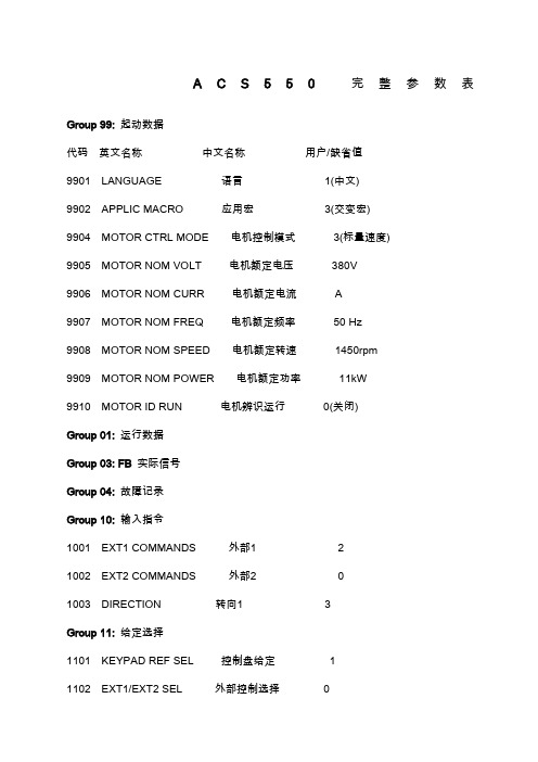
A C S550完整参数表Group 99: 起动数据代码英文名称中文名称用户/缺省值9901 LANGUAGE 语言1(中文)9902 APPLIC MACRO 应用宏3(交变宏)9904 MOTOR CTRL MODE 电机控制模式3(标量速度)9905 MOTOR NOM VOLT 电机额定电压380V9906 MOTOR NOM CURR 电机额定电流 A9907 MOTOR NOM FREQ 电机额定频率50 Hz9908 MOTOR NOM SPEED 电机额定转速1450rpm9909 MOTOR NOM POWER 电机额定功率11kW9910 MOTOR ID RUN 电机辨识运行0(关闭)Group 01: 运行数据Group 03: FB 实际信号Group 04: 故障记录Group 10: 输入指令1001 EXT1 COMMANDS 外部1 21002 EXT2 COMMANDS 外部2 01003 DIRECTION 转向1 3Group 11: 给定选择1101 KEYPAD REF SEL 控制盘给定 11102 EXT1/EXT2 SEL 外部控制选择01103 REF1 SELECT 给定值1选择 11104 REF1 MIN 给定值1下限0Hz/0rpm1105 REF1 MAX 给定值1上限50 Hz /1500 rpm 1106 REF2 SELECT 给定值2选择 21107 REF2 MIN 给定值2下限0%1108 REF2 MAX 给定值2上限100%Group 12: 恒速运行1201 CONST SPEED SEL 恒速选择91202 CONST SPEED 1 恒速1 300rpm/5Hz 1203 CONST SPEED 2 恒速2 600rpm/10Hz 1204 CONST SPEED 3 恒速3 900rpm/15Hz 1205 CONST SPEED 4 恒速4 1200rpm/20Hz 1206 CONST SPEED 5 恒速5 1500rpm/25Hz 1207 CONST SPEED 6 恒速6 2400rpm/40 Hz 1208 CONST SPEED 7 恒速7 3000rpm/50 Hz 1209 TIMED MODE SEL 定时模式选择 2Group 13: 模拟输入Group 14: 继电器输出1401 RELAY OUTPUT 1 继电器输出1 11402 RELAY OUTPUT 2 继电器输出2 21403 RELAY OUTPUT 3 继电器输出3 31404 RO 1 ON DELAY 继电器1 0s1405 RO 1 OFF DELAY 继电器1 0s1406 RO 2 ON DELAY 继电器2 0s1407 RO 2 OFF DELAY 继电器2 0s1408 RO 3 ON DELAY 继电器3 0s1409 RO 3 OFF DELAY 继电器3 0s1410 RELAY OUTPUT 4 继电器输出4 01411 RELAY OUTPUT 5 继电器输出5 01412 RELAY OUTPUT 6 继电器输出6 01413 RO 4 ON DELAY 继电器4通延时0s1414 RO 4 OFF DELAY 继电器4断延时0s1415 RO 5 ON DELAY 继电器5通延时0s1416 RO 5 OFF DELAY 继电器5断延时0s1417 RO 6 ON DELAY 继电器6通延时0s1418 RO 6 OFF DELAY 继电器6断延时0sGroup 15: 模拟输出1501 AO1 CONTENT SEL AO1赋值1031502 AO1 CONTENT MIN AO1赋值下限取决于参数0103 1503 AO1 CONTENT MAX AO1赋值上限取决于参数0103 1504 MINIMUM AO1 AO1下限0 mA1505 MAXIMUM AO1 AO1 上限0 mA1506 FILTER AO1 AO1 滤波时间0.1 s1507 AO2 CONTENT SEL AO2 赋值1041508 AO2 CONTENT MIN AO2 赋值下限取决于参数0104 1509 AO2 CONTENT MAX AO2 赋值上限取决于参数01041510 MINIMUM AO2 AO2 下限0 mA 1511 MAXIMUM AO2 AO2 上限0 mA 1512 FILTER AO2 AO2 滤波时间0.1 s Group 16: 系统控制1601 RUN ENABLE 运行允许01602 PARAMETER LOCK 参数锁定 11603 PASS CODE 解锁密码01604 FAULT RESET sEL 故障复位选择01605 USER PAR SET CHG用户参数切换01606 LOCAL LOCK 本地锁定01607 PARAM SAVE 参数存储01608 START ENABLE 1 起动允许1 01609 START ENABLE 2 起动允许2 01610 DISPLAY ALARMS 显示报警0Group 20: 限幅2001 MINIMUM SPEED 最小转速0rpm 2002 MAXIMUM SPEED 最大转速1500 rpm 2003 MAX CURRENT 最大电流 1.8 * I2hd 2005 OVERVOLT CTRL 过压控制 12006 UNDERVOLT CTRL 欠压控制 12007 MINIMUM FREQ 最小频率0 Hz 2008 MAXIMUM FREQ 最大频率50 Hz 2013 MIN TORQUE SEL 最小转矩选择02014 MAX TORQUE SEL 最大转矩选择0 2015 MIN TORQUE 1 最小转矩1 -300.0% 2016 MIN TORQUE 2 最小转矩2 -300.0% 2017 MAX TORQUE 1 最大转矩1 300.0% 2018 MAX TORQUE 2 最大转矩2 300.0% Group 21: 起动/ 停止2101 START FUNCTION 起动方式 1 2102 STOP FUNCTION 停车方式 12103 DC MAGN TIME 直流磁化时间0.3s 2104 DC CURR CTL 直流抱闸控制02105 DC HOLD SPEED 直流抱闸转速rpm 2106 DC CURR REF 直流抱闸电流30% 2107 DC BRAKE TIME 直流制动时间0 s 2108 START INHIBIT 起动禁止02109 EM STOP SEL 急停选择02110 TORQ BOOST CURR 转矩提升电流100% Group 22: 加速/ 减速2201 ACC/DEC 1/2 SEL 加减速曲线选择 52202 ACCELER TIME 1 加速时间1 5s 2203 DECELER TIME 1 加速时间1 5s 2204 RAMP SHAPE 1 速度曲线形状1 0.0s 2205 ACCELER TIME 2 加速时间2 60 s 2206 DECELER TIME 2 加速时间2 60 s2207 RAMP SHAPE 2 速度曲线形状2 0.0 s 2208 EM DEC TIME 急停减速时间 1.0 s2209 RAMP INPUT 0 积分器输入置零0Group 23: 速度控制2301 PROP GAIN 比例增益102302 INTEGRATION TIME 积分时间 2.52303 DERIVATION TIME 微分时间02304 ACC COMPENSATION 加速补偿02305 AUTOTUNE RUN 自优化运行0( 关闭) Group 24: 转矩控制2401 TORQ RAMP UP 转矩上升时间0s2402 TORQ RAMP DOWN 转矩下降时间0s Group 25: 危险频率Group 26: 电机控制2601 FLUX OPTIMIZATION 允许磁通最优化0关闭2602 FLUX BRAKING 磁通制动0关闭2603 IR COMP VOLT IR 补偿电压取决于容量2604 IR COMP FREQ IR 补偿电频率80%2605 U/F RATIO 压频比曲线1(线性)2606 SWITCHING FREQ 开关频率4kHz 2607 SW FREQ CTRL 开关频率控制1(打开)2608 SLIP COMP RATIO 滑差补偿02609 NOISE SMOOTHING 噪音过滤0(禁止)Group 29: 维护2901 COOLING FAN TRIG 冷却风机触发点0(未选择) 2902 COOLING FAN ACT 冷却风机计数器0.0 kh 2903 REVOLUTION TRIG 累计转数触发点0 (未选择) 2904 REVOLUTION ACT 累计转数计数器0 MRev 2905 RUN TIME TRIG 运行时间触发点0 (未选择) 2906 RUN TIME ACT 运行时间计数器0.0 kh 2907 USER MWH TRIG 累计功耗触发点0 (未选择) 2901 USER MWH ACT 累计功耗计数器0.0 MWh Group 30: 故障功能3001 AI<MIN FUNCTION AI 故障03002 PANEL COMM ERR 控制盘丢失 13003 EXTERNAL FAULT 1 外部故障1 03004 EXTERNAL FAULT 2 外部故障2 03005 MOT THERM PROT 电机温度保护1(故障) 3006 MOT THERM TIME 电机温升时间500 s 3007 MOT LOAD CURVE 电机负载曲线100% 3008 ZERO SPEED LOAD 零速负载70% 3009 BREAK POINT FREQ 负载折点35 Hz 3010 STALL FUNCTION 堵转功能0 (未选择) 3011 STALL FREQUENCY 堵转频率20 Hz 3012 STALL TIME 堵转时间20 s3013 UNDERLOAD FUNC 欠载功能0(未选择)3014 UNDERLOAD TIME 欠载时间20 s 3015 UNDERLOAD CURVE 欠载曲线 13017 EARTH FAULT 接地故障1(允许) 3018 COMM FAULT FUNC 通讯故障功能0(未选择) 3019 COMM FAULT TIME 通讯故障时间 3.0 s 3021 AI1 FAULT LIMIT AI1故障极限0%3022 AI2 FAULT LIMIT AI2故障极限0%3023 WIRING FAULT 接线故障1允许Group 31: 自动复位3101 NR OF TRIALS 复位次数03102 TRIAL TIME 复位时间30s3103 DELAY TIME 延时时间0s3104 AR OVERCURRENT 过流复位0( 禁止) 3105 AR OVERVOLTAGE 过压复位0( 禁止) 3106 AR UNDERVOLTAGE 欠压复位0( 禁止) 3107 AR AI<MIN AI 故障复位0(禁止) 3108 AR EXTERNAL FLT 外部故障复位0(禁止) Group 32: 监控器Group 33: 信息Group 34: 控制盘显示/ 过程变量Group 35: 电机温度测量3501 SENSOR TYPE 传感器类型03502 INPUT SELECTION 输入选择 13503 ALARM LIMIT 报警极限Ohm / 0 3504 FAULT LIMIT 故障极限Ohm / 0 Group 36: 定时器功能Group 40: 过程PID 设置14001 GAIN 增益 1.04002 INTEGRATION TIME 积分时间60s 4003 DERIVATION TIME 微分时间0s4004 PID DERIV FILTER 微分滤波1s4005 ERROR VALUE INV 偏差值取反0否4006 UNITS 单位 44007 UNIT SCALE 显示格式 14008 0% VALUE 0% 值0.0% 4009 100% VALUE 100% 值100% 4010 SET POINT SEL 给定值选择 14011 INTERNAL SETPNT 内部给定值40.0% 4012 SETPOINT MIN 给定最小值0%4013 SETPOINT MAX 给定最大值100% 4014 FBK SEL 反馈值选择 14015 FBK MULTIPLIER 乘法因子0(未使用) 4016 ACT1 INPUT 实际值1 输入 24017 ACT2 INPUT 实际值2 输入 24018 ACT1 MINIMUM 实际值1 下限0% 4019 ACT1 MAXIMUM 实际值1 上限100%4020 ACT2 MINIMUM 实际值2 下限0% 4021 ACT2 MAXIMUM 实际值2 上限100% 4022 SLEEP SELECTION 睡眠选择04023 PID SLEEP LEVEL 睡眠频率0 Hz 4024 PID SLEEP DELAY 睡眠延时60s 4025 WAKE-UP DEV 唤醒偏差4026 WAKE-UP DELAY 唤醒延时0.50s 4027 PID 1 PARAM sET PID1参数选择0 Group 41: 过程PID 设置24101 GAIN 增益 1.04102 INTEGRATION TIME 积分时间60s 4103 DERIVATION TIME 微分时间0s 4104 PID DERIV FILTER 微分滤波1s4105 ERROR VALUE INV 偏差值取反0否4106 UNITS 单位 44107 UNIT SCALE 显示格式 14108 0% VALUE 0%值0.0% 4109 100% VALUE 100% 值100% 4110 SET POINT SEL 给定值选择 14111 INTERNAL SETPNT 内部给定值40.0% 4112 SETPOINT MIN 给定最小值0% 4113 SETPOINT MAX 给定最大值100% 4114 FBK SEL 反馈值选择 14115 FBK MULTIPLIER 乘法因子0(未使用) 4116 ACT1 INPUT 实际值1输入 24117 ACT2 INPUT 实际值2输入 24118 ACT1 MINIMUM 实际值1下限0% 4119 ACT1 MAXIMUM 实际值1上限100% 4120 ACT2 MINIMUM 实际值2下限0% 4121 ACT2 MAXIMUM 实际值2上限100% 4122 SLEEP SELECTION 睡眠选择04123 PID SLEEP LEVEL 睡眠频率0Hz 4124 PID SLEEP DELAY 睡眠延时60s 4125 WAKE-UP DEV 唤醒偏差4126 WAKE-UP DELAY 唤醒延时0.50 s Group 42: 外部/ 修正PID4201 GAIN 增益 1.04202 INTEGRATION TIME 积分时间60s 4203 DERIVATION TIME 微分时间0s4204 PID DERIV FILTER 微分滤波1s4205 ERROR VALUE INV 偏差值取反04206 UNITS 单位 44207 UNIT SCALE 显示格式 14208 0% VALUE 0%值0% 4209 100% VALUE 100% 值100% 4210 SET POINT SEL 给定值选择 14211 INTERNAL SETPNT 内部给定值40.0%4212 SETPOINT MIN 给定最小值0%4213 SETPOINT MAX 给定最大值100%4214 FBK SEL 反馈值选择 14215 FBK MULTIPLIER 乘法因子0(未使用)4216 ACT1 INPUT 实际值1输入 24217 ACT2 INPUT 实际值2 输入 24218 ACT1 MINIMUM 实际值1下限0%4219 ACT1 MAXIMUM 实际值1上限100%4220 ACT2 MINIMUM 实际值2下限0%4221 ACT2 MAXIMUM 实际值2上限100%4228 ACTIVATE 激活04229 OFFSET 偏置04230 TRIM MODE 修正模式04231 TRIM SCALE 修正因子0%4232 CORRECTION SRC 纠偏源1(PID2 给定) Group 51: 外部通讯模块Group 52: 控制盘通讯Group 53: 内置通讯协议Group 81: PFC 控制8103 REFERENCE STEP1 给定增量1 0%8104 REFERENCE STEP2 给定增量2 0%8105 REFERENCE STEP3 给定增量3 0%8109 START FREQ 1 起动频率1 50Hz8110 START FREQ 2 起动频率2 50Hz8111 START FREQ 3 起动频率3 50Hz8112 LOW FREQ 1 停止频率1 25Hz8113 LOW FREQ 2 停止频率2 25Hz8114 LOW FREQ 3 停止频率3 25Hz8115 AUX MOT START D 辅机起动延时5s8116 AUX MOT STOP D. 辅机停止延时 3 s8117 NR OF AUX MOT 辅机数量 18118 AUTOCHNG INTERV 自动切换间隔0( 未选择) 8119 AUTOCHNG LEVEL 自动切换范围50%8120 INTERLOCKS 内部锁定 48121 REG BYPASS CTRL 调节器旁路0( 否) 8122 PFC START DELAY PFC起动延时0.5 s8123 PFC ENABLE PFC 允许0( 未选择) 8124 ACC IN AUX STOP 辅机停止时加速0 ( 未选择) 8125 DEC IN AUX START 辅机起动时减速00 ( 未选择) 8126 TMED AUTOCHNG 定时切换0( 未选择) 8127 MOTORS 电机个数0( 未选择) Group 98: 可选件。