SY89230UMG;SY89230UMG TR;中文规格书,Datasheet资料
AMD微雾分离器系列商品介绍说明书

SymbolAMDMicro Mist SeparatorSeries AMDCan separate and remove aerosol state oil mist in compressed air and remove particles such as carbon or dust of more than 0.01 μm.Use this product as a pre-filter for compressed air for precision instruments or clean room requiring higher clean air.Specifications0.05 MPa 1.5 MPa FluidMax. operating pressure Min. operating pressure ∗Proof pressureAmbient and fluid temperature Nominal filtration rating Element lifeCompressed air1.0 MPa 5 to 60°C0.01 μm (Filtration efficiency: 99.9%)Oil mist density at outlet Max. 0.1 mg/m 3 (ANR)∗(Before saturated with oil, less than 0.01 mg/m 3 (ANR) ≈0.008 ppm)2 years (1 year for flange type)or when pressure drop reached 0.1 MPa∗ With auto drain: 0.1 MPa (N.O. type) or 0.15 MPa (N.C. type)∗ Oil mist density at 30 mg/m 3 (ANR) blown out by compressor.Modular connection is possible with AMD150C to 550C.(For details, refer to page 61.)AMD150C to 550C AMD650/850Made to Order(For details, refer to page 67.)CautionBe sure to read this before handling.Refer to back pages 1 and 2 for Safety Instructions, “Precautions for Handling Pneumatic Devices” (M-03-E3A) for Common Precautions, and back pages 3 through to 7 for Specific Product Precautions.o u r t e s y o f C M A /F l o d y n e /H y d r a d y n e ▪ M o t i o n C o n t r o l ▪ H y d r a u l i c ▪ P n e u m a t i c ▪ E l e c t r i c a l ▪ M e c h a n i c a l ▪ (800) 426-5480 ▪ w w w .c m a f h .c o mHow to Order OptionsSeries AMD ourtesyofCMA/Flodyne/Hydradyne▪MotionControl▪Hydraulic▪Pneumatic▪Electrical▪Mechanical▪(8)426-548▪www.cmafh.comHow to OrderA M D 10A M D 90, 91A M D 850A M D 80 , 81A M D 650A M D 550C A M D 450C A M D 350CA M D 250CA M D 150CAMD 65010Free standing type AMD800/810 to 10 0Piping support type 2000AMD 82001AMD 8Maximum Air FlowMax. flow lineModel SelectionSelect a model in accordance with the following procedure taking the inlet pressure and the max. air flow rate into consideration.(Example) Inlet pressure: 0.6 MPaMax. air flow rate: 5 m 3/min (ANR)1.Obtain the intersecting point A of inlet pressure and max. air flow rate in the graph.2. The AMD650 is obtained when the max. flow line is above the in-tersecting point A in the graph.Body size8910Body size89DescriptionWith differential pressure gauge (GD40-2-01)With differential pressure switch(With indicator, 125 VAC, 30 VDC)With IN-OUT flangeWith differential pressure gauge(GD40-2-01) and IN-OUT flangeN.C., N.O. auto drain, drain piping type White vaseline specificationsPage for details —P.68P.68P.69P.69X6X37X15X17P.70P.70X26X12Symbol Made to Order(“How to Order” and the applicable models are different from those shown on this page. Be sure to refer to “Made to Order”.)—Nil60150(6B)JIS 10K FF flange2050(2B)JIS 10K FF flange 3080(3B)JIS 10K FF flange 40100(4B)JIS 10K FF flange Port sizeSizeApplicable body sizeAMD800, 810AMD9 0AMD10 0Symbol00With manual drain cock 10With auto drainTypeDescription SymbolThread typeNilRc F G NNPTType Symbol Type01With manual drain cock 11With auto drainDescriptionSymbolAuto drain specifications/Option Auto drain specifications Option Option Auto drain specificationsD J R DJ T R Applicable modelAMD650AMD850N.O. auto drainDrain guide IN-OUT reversal directionTWith element service indicator14Auto Drain Specifications/Option Combinations: Available: Not availablePort size10142011122SizeApplicable body size650850Symbol Body size650850∗1Bracket is included,(but not assembled).AccessoryDescription —Bracket ∗1Symbol BNil Auto drain ∗2DescriptionDrain cock (Without auto drain) ∗3N.O. auto drainSymbol DNil∗2 Refer to “Auto Drain Specifications/Option Combinations”.∗3Body size 850 is equipped with a ball valve (Rc3/8 femalethreaded). Mount a piping adapter IDF-AP609 (page 62) to the ball valve if NPT3/8 female threaded is required.With element service indicatorOption ∗2Drain guide female threaded ∗4IN-OUT reversal direction 14Description—TJ R Symbol Nil∗4Drain piping and piping for a stopvalve such as ball valve are required.AMD650/850AMD801/811/9 1Port size2050(2B)JIS 10K FF flange 3080(3B)JIS 10K FF flange 40100(4B)JIS 10K FF flangeSizeApplicable body sizeAMD8 1AMD9 1SymbolNote)Make sure to select a model that has the max. flow line abovethe obtained intersecting point. With a model that has the max. flow line below the obtained intersecting point, the flow rate will be exceeded, thus leading to a problem such as being unable to satisfy the specifications.M a x . a i r f l o w r a t e (m 3/m i n (A N R ))Note) Refer to “How to Order BowlAssembly” on page 63.Micro Mist Separator SeriesAMDo u r t e s y o f C M A /F l o d y n e /H y d r a d y n e ▪ M o t i o n C o n t r o l ▪ H y d r a u l i c ▪ P n e u m a t i c ▪ E l e c t r i c a l ▪ M e c h a n i c a l ▪ (800) 426-5480 ▪ w w w .c m a f h .c o mAMD150C AMD250C AMD350C AMD450C AMD850AMD80 /81AMD650AMD10 0AMD550C AMD9 0/9 1Note) Compressed air over max. flow line in the table below may not meet the specifications of the product.It may cause damage to the element.Flow Characteristics /Select the model taking the max. flow capacity into consideration. ( Element oil saturation Initial condition)P r e s s u r e d r o p (M P a )Air flow rate (l /min (ANR))P r e s s u r e d r o p (M P a )Air flow rate (l /min (ANR))P r e s s u r e d r o p (M P a )Air flow rate (m 3/min (ANR))P r e s s u r e d r o p (M P a )Air flow rate (l /min (ANR))P r e s s u r e d r o p (M P a )Air flow rate (l /min (ANR))P r e s s u r e d r o p (M P a )Air flow rate (l /min (ANR))P r e s s u r e d r o p (M P a )Air flow rate (m 3/min (ANR))P r e s s u r e d r o p (M P a )P r e s s u r e d r o p (M P a )P r e s s u r e d r o p (M P a )Air flow rate (m 3/min (ANR))Max. flow lineMax. flow lineMax. flow lineMax. flow lineMax. flow lineMax. flow lineMax. flow lineMax. flow lineMax. flow lineMax. flow lineSeries AMDo u r t e s y o f C M A /F l o d y n e /H y d r a d y n e ▪ M o t i o n C o n t r o l ▪ H y d r a u l i c ▪ P n e u m a t i c ▪ E l e c t r i c a l ▪ M e c h a n i c a l ▪ (800) 426-5480 ▪ w w w .c m a f h .c o mIN OUTElementConstructionAMD150C to 550C, AMD650AMD850AMD80 /81 /9 0/9 1/10 0OUTIN ∗ Element assembly: With gasket (1 pc.) and O-ring (1 pc.)∗ Refer to back page 6 for replacement of auto drain.∗ Element assemblies for Made to Order (X6, X12, X15, X17, X20, X26, X37) are same as those for standard (see the above table).∗ The AMD850 is aluminum casted.Note) Sight glass is indicated in the figure for easy understanding ofcomponent parts. However, it differs from the actualconstruction. Refer to dimensions on pages 31 through to 34 for details.Micro Mist Separator SeriesAMDo u r t e s y o f C M A /F l o d y n e /H y d r a d y n e ▪ M o t i o n C o n t r o l ▪ H y d r a u l i c ▪ P n e u m a t i c ▪ E l e c t r i c a l ▪ M e c h a n i c a l ▪ (800) 426-5480 ▪ w w w .c m a f h .c o mAMD150C to 550CC: With auto drain (N.C.)D: With auto drain (N.O.)OptionJ: Drain guide 1/4 female threadedCombination of D: With auto drain (N.O.) S, U: With differential pressure switch (with indicator)T: With element service indicatorDimensionsSeries AMDo u r t e s y o f C M A /F l o d y n e /H y d r a d y n e ▪ M o t i o n C o n t r o l ▪ H y d r a u l i c ▪ P n e u m a t i c ▪ E l e c t r i c a l ▪ M e c h a n i c a l ▪ (800) 426-5480 ▪ w w w .c m a f h .c o m18076853111601502015114.512136160402533341032205537M a i n t e n a n c e s p a c eAMD150C to 550C, AMD650T: With element service indicatorDrainINOUTINOUT(Accessory)Bracket Auto drainD: With auto drain (N.O.)OptionJ: Drain guide 1/4 female threaded201/4 female threaded34Drain cock: Blackø10 one-touch fittingDimensionsMicro Mist Separator SeriesAMDo u r t e s y o f C M A /F l o d y n e /H y d r a d y n e ▪ M o t i o n C o n t r o l ▪ H y d r a u l i c ▪ P n e u m a t i c ▪ E l e c t r i c a l ▪ M e c h a n i c a l ▪ (800) 426-5480 ▪ w w w .c m a f h .c o m22011061818422022018024131530348464101204246158Rc 3/8 female threadedM a i n t e n a n c e s p a c e DrainBracket (Accessory)2 x port sizeAMD850T: With element service indicatorAuto drainD: With auto drain (N.O.)for AMD850Option233/8 female threadedDimensionsSeries AMDOUTININ OUTo u r t e s y o f C M A /F l o d y n e /H y d r a d y n e ▪ M o t i o n C o n t r o l ▪ H y d r a u l i c ▪ P n e u m a t i c ▪ E l e c t r i c a l ▪ M e c h a n i c a l ▪ (800) 426-5480 ▪ w w w .c m a f h .c o mLabelLabelDrain≈≈ORIENTATIONORIENTATIONAMD801/811/9 1AMD800/810/9 0/10 0Model500A720M16 x l 400Anchor bolt M20 x l 500AMD800/810AMD9 0Connection (Flange)50(2B), 80(3B)JIS 10K FF flange50(2B), 80(3B), 100(4B)JIS 10K FF flange 100(4B), 150(6B)JIS 10K FF flange870M20 x l 500AMD10 0300øB 560745200(8B)øC 400550300D3003001300E 132013801430F 148016101520G 1585174020H2424ModelConnection (Flange)50(2B)JIS 10K FF flange50(2B), 80(3B), 100(4B)JIS 10K FF flange400A620AMD801/811AMD9 1280øB 445150(6B)øC 300(12B)760D795150E300270F5201033G13183H3887J9723 x øH holesDimensionsMicro Mist Separator SeriesAMDIN OUTIN OUTOUT INOUTINOUTo u r t e s y o f C M A /F l o d y n e /H y d r a d y n e ▪ M o t i o n C o n t r o l ▪ H y d r a u l i c ▪ P n e u m a t i c ▪ E l e c t r i c a l ▪ M e c h a n i c a l ▪ (800) 426-5480 ▪ w w w .c m a f h .c o m。
Moxa UC-8100-ME-T系列臂型无线可插拔工业电脑说明书

UC-8100-ME-T SeriesArm-based wireless-enabled DIN-rail industrial computer with2serial ports and2LAN portsFeatures and Benefits•Armv7Cortex-A81000MHz processor•Dual auto-sensing10/100Mbps Ethernet ports•SD slot for storage expansion•Programmable LEDs and a programmable button for easy installation andmaintenance•Mini PCIe slot for cellular module•Cybersecurity functions•Debian9open platform•-40to70°C wide-temperature range with LTE enabledCertificationsIntroductionThe UC-8100-ME-T computing platform is designed for embedded data acquisition applications.The computer comes with dual RS-232/422/485 serial ports and dual10/100Mbps Ethernet ports,as well as a Mini PCIe socket to support cellular modules.These versatile capabilities let users efficiently adapt the UC-8100-ME-T to a variety of complex communications solutions.The UC-8100-ME-T is built around a Cortex-A8processor that has been optimized for use in energy monitoring systems,but is widely applicable to a variety of industrial solutions.With flexible interfacing options,this tiny embedded computer is a reliable and secure gateway for data acquisition and processing at field sites as well as a useful communications platform for many other large-scale deployments.Wide-temperature and LTE-enabled models are available.All units are thoroughly tested in a testing chamber,guaranteeing that the LTE-enabled computing platforms are suitable for wide-temperature applications.AppearanceSpecificationsComputerCPU Armv7Cortex-A81GHzDRAM UC-8112-ME-T-LX Series:512MB DDR3UC-8112-ME-T-LX1Series:1GB DDR3Pre-installed OS Linux Debian9(kernel v4.4)Storage Pre-installed4GB eMMCComputer InterfaceUSB2.0USB2.0hosts x1,type-A connectorsExpansion Slots mPCIe slot x1Number of SIMs1SIM Format MiniButtons Reset buttonEthernet InterfaceEthernet Ports Auto-sensing10/100Mbps ports(RJ45connector)x2 Magnetic Isolation Protection N/A,1.5kV(built-in)LED IndicatorsSystem Power x1SD slots x1Programmable x4Wireless Signal Strength Cellular/Wi-Fi x3Serial InterfaceSerial Ports2x RS-232/422/485Console Port1x4-pin header to DB9console portData Bits5,6,7,8Parity None,Even,Odd,Space,MarkStop Bits1,1.5,2Serial SignalsRS-232TxD,RxD,RTS,CTS,DTR,DSR,DCD,GNDRS-422Tx+,Tx-,Rx+,Rx-,GNDRS-485-2w Data+,Data-,GNDRS-485-4w Tx+,Tx-,Rx+,Rx-,GNDPower ParametersInput Voltage12to36VDCInput Current500mA@12VACPower Consumption6WReliabilityAlert Tools External RTC(real-time clock)Automatic Reboot Trigger External WDT(watchdog timer)Physical CharacteristicsHousing MetalDimensions141x125.6x54.8mm(5.55x4.94x2.15in)Weight550g(1.22lb)Installation DIN-rail mounting,Wall mounting(with optional kit)Environmental LimitsOperating Temperature UC-8112-ME-T-LX/8112-ME-T-LX1:-40to85°C(-40to185°F)UC-8112-ME-T-LX-US-LTE/8112-ME-T-US-LTE-LX1:-40to70°C(-40to158°F) Storage Temperature(package included)-40to85°C(-40to185°F)Ambient Relative Humidity5to95%(non-condensing)Vibration2Grms@IEC60068-2-64,random wave,5-500Hz,1hr per axis(without any USBdevices attached)Shock IEC60068-2-27Standards and CertificationsSafety UL60950-1EMC EN55032/24EMI CISPR32,FCC Part15B Class AEMS IEC61000-4-2ESD:Contact:8kV;Air:15kVIEC61000-4-3RS:80MHz to1GHz:20V/mIEC61000-4-4EFT:Power:4kV;Signal:4kVIEC61000-4-5Surge:Power:1kVIEC61000-4-6CS:10VIEC61000-4-8PFMFGreen Product RoHS,CRoHS,WEEEHazardous Locations Class I Division2MTBFTime535,916hrsStandards Telcordia(Bellcore)StandardWarrantyWarranty Period5yearsDetails See /warrantyPackage ContentsDevice1x UC-8100-ME-T Series computerInstallation1x power jack,1x DIN-rail kit(preinstalled)Documentation1x quick installation guide1x warranty cardDimensionsOrdering InformationModel Name CPU RAM Storage US LTE Module Built-In Operating Temp. UC-8112-ME-T-LX Armv7Cortex-A81GHz512MB4GB eMMC–-40to70°C UC-8112-ME-T-LX-US-LTE Armv7Cortex-A81GHz512MB4GB eMMC✓-40to85°C UC-8112-ME-T-LX1Armv7Cortex-A81GHz1GB4GB eMMC–-40to85°C UC-8112-ME-T-US-LTE-LX1Armv7Cortex-A81GHz1GB4GB eMMC✓-40to70°CAccessories(sold separately)Desktop Mounting KitsANT-GPS-OSM-05-3M1572MHz,active GPS antenna,26dBi,for GPS applications,3m cableANT-LTE-ASM-04BK704-960/1710-2620MHz,LTE omni-directional stick antenna,4.5dBiANT-LTE-ASM-05BK704-960/1710-2620MHz,LTE stick antenna,5dBiANT-LTE-OSM-03-3m BK700-2700MHz,multi-band antenna,specifically designed for2G,3G,and4G applications,3m cable ANT-LTE-OSM-06-3m BK MIMO700-2700/2400-2500/5150-5850MHz,multi-band antenna,3m cableCablesCBL-F9DPF1x4-BK-100Console cable with4-pin connector,1mPower CordsPWC-C7AU-2B-183Power cord with Australian(AU)plug,2.5A/250V,1.83mPWC-C7CN-2B-183Power cord with two-prong China(CN)plug,1.83mPWC-C7EU-2B-183Power cord with Continental Europe(EU)plug,2.5A/250V,1.83mPWC-C7UK-2B-183Power cord with United Kingdom(UK)plug,2.5A/250V,1.83mPWC-C7US-2B-183Power cord with United States(US)plug,10A/125V,1.83mPower AdaptersPWR-24270-DT-S1Power adapter,input voltage90to264VAC,output voltage24V with2.5A DC loadWall-Mounting KitsWALLMOUNT-8100-01Wall-mounting kit for the UC-8100DIN-Rail Mounting KitsDK-25-01DIN-rail mounting kit,2screwsCellular Wireless ModulesCELLULAR-LTE-US Cellular module,i-PEX MHF to SMA adapter,Mini PCI/e mount,2screwsME-CELLULAR-LTE-EU LTE Cat.3module for Europe,2SMA connectors with cableWi-Fi Wireless ModulesWi-Fi-BGN Wi-Fi module,2SMA connectors with cable©Moxa Inc.All rights reserved.Updated May31,2019.This document and any portion thereof may not be reproduced or used in any manner whatsoever without the express written permission of Moxa Inc.Product specifications subject to change without notice.Visit our website for the most up-to-date product information.。
ASM_AD892HS
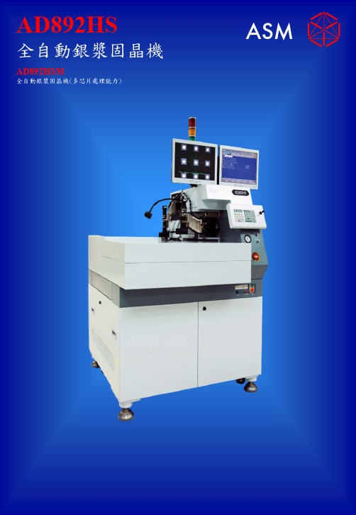
記憶容量
底板數量 焊點數量/底板
500 2,000
焊頭
吸咀 焊接壓力
表面吸取類形 30 - 250 g
工件工作台
行程範圍 XY分辨率
16” x 4” (406 mm x 101mm) 0.05 mil (1.25µm)
* 機件技術之㈾料,若經修改,怒不另行通知 * 實際表現會因產品而㈲斦改變
芯片系統
Kaohsiung 高雄 Tel : 886-7-367 6300 Fax : 886-7-367 6399
Hsin Chu 新竹 Tel : 886-3-543 1500 Fax : 886-3-543 1555
/
Philippines 菲律賓 Tel : 63-2-850 4543 Fax : 63-2-850 4547
Shenzhen 深圳 Tel : 86-755-8830 8533 Fax : 86-755-8344 6245
China ㆗國 Xiamen 廈門 Tel : 86-592-5509 125 Fax : 86-592-5509 121
Dongguan 東莞 Tel : 86-769-7125 600 Fax : 86-769-7125 601
所需設施
電壓 頻率 壓縮空氣 消耗壓縮空氣 功率消耗
100 - 240 VAC (工廠預先設定) 50/60 Hz (工廠預先設定) 5 bar 180 LPM 1,500 W
體積及重量
AD892HS
寬x深x高 115
ASM
For further information, please contact our regional offices
AD892HS
全㉂動銀漿固晶機
三友SY18TF-0025-0500-001 产品规格确认书说明书

电话Tel:(86)-769-82618888传真Fax:(86)-769-85914553网址Web site:产品规格确认书Specification for approval文件编号File No:变更版记录Revisions版本Version No.变更内容Change description变更原因Reason日期Date修改Drafted by审核Checked byV1.0初版/2022.12.12邹一鸣黄玉华目录Catalog1,外形尺寸(Outerdimensions)(单位:mm)2,推荐PCB 安装尺寸(Suggested PCBlayout)(单位:mm)3,原理图(Schematicdiagram)4,绕线参数(Winding parameter)备注:绕线圈数参考,以电感量为准。
The turns of coil specified below is only for reference,the actual number is decided by the inductance起线-尾线Start-finished pin线径规格Wire diameter 圈数Turns 绕线方式Winding condition胶带圈数Turns of tape1-42UEW F 0.55mm 26(REF)close \2-32UEW F 0.55mm26(REF)close\5,产品工艺要求(Technological requirements):1)绕线平整,两个绕组圈数相同。
The turns of two coils must be same,and the windingshall be flat without overlap.2)磁芯,隔板和底座点胶固定。
Fasten core and bobbin with glue.3)如客户无要求,产品标签为SY-2.5A-5mH否则按照客户要求if norerequirements,marked the inductor with:SY-2.5A-5mH,else meets custormer’s specfication.6,电气特性(Electrical characteristics)项目Item 测试引脚Pin NO.规格SPEC.测试条件Conditions电感Inductance 1-45mH±30%10KHz0.1mA20℃(LCR测试仪器内阻100Ω)2-35mH±30%电感偏差Inductance deviation ||1-4|-|2-3||500uH max10KHz50mV20℃(LCR测试仪器内阻100Ω)漏感Leakage inductance 1-4300uH max10KHz50mV20℃(LCR测试仪器内阻100Ω)直流电阻DC resistance 1-495mΩmax20℃2-395mΩmax高压测试Hi-pot test(1-4)-(2-3) 1.5KV2S1mA 额定电压Rated Voltage250V MAX.50HZ 绝缘电阻Insulationresistance(1-4)-(2-3)100MΩmin500VDC 工作温度范围Operation Temperature -40~125℃包含线圈发热导致的温度升高(includingcoil’s temperature rising)7,材料表(Material list)编号NO.类别Description材料Material供应商MANUFACTURERUL NO.温度等级TEMP.1Core T18*10*10CGh7NANTONG GUANYOUDAMAGNETIC INDUSTRYCO.LTD/130℃SHANDONG KAITONGELECTRON CO.,LTD/130℃2Case PM-9820SUMITOMO BAKELITE COLTDE41429150℃T375HFCHANGCHU PLASTICSCO.,LTDE59481150℃3Wire2UEW FGuangdong JinyanElectrotechnics orequivalentE238500155℃4Epoxy EP600Santong orequivalent/130℃5Solder Sncu Qiandao orequivalent//8,推荐焊接条件(Recommend soldering conditions)1)焊接方式:波峰焊(wave soldering)2)典型焊接曲线(Classification wave soldering profile)9.可靠性测试条件(Reliability Testing Conditions)序号(NO.)测试项目(Item)试验条件(Conditions)判定标准(Criterion)1高温存储Hightemperaturestorage125℃300小时125℃300Hours室温放置2h后,各项性能满足规格书要求After2hours at room temperature,theperformance meets the requirements ofthe specifications2低温存储Low temperaturestorage-40℃300小时-40℃300Hours室温放置2h后,各项性能满足规格书要求After2hours at room temperature,theperformance meets the requirements ofthe specifications3冷热冲击Thermal shock-40℃30分钟~125℃30分钟10个循环-40℃30minutes~125℃30minutes10cycles室温放置2h后,各项性能满足规格书要求After2hours at room temperature,theperformance meets the requirements ofthe specifications4湿热试验Damp heat test温度40℃,湿度93%RH240小时Temperature40℃humidity93%RH240hours室温放置2h后,各项性能满足规格书要求After2hours at room temperature,theperformance meets the requirements ofthe specifications5电寿命试验Life test额定电流2.5A1000小时Rated current2.5A1000Hours试验完成后,各项性能满足规格书要求After the test,the performance meetsthe requirements of thespecifications。
892松川系列继电器

30G
Damage limits
100G
Mechanical
10,000,000 operations (frequency 1800 operations/hr)
Electrical
100,000 operations (frequency 900 operations/hr)
-40 ~ +85℃ (no freezing)
10A/5A 125VAC
5A/3A 277VAC
7A/5A 277VAC
TV-3
TUV Pending
TUV
892
892H
7A/3A 120VAC 5A/3A 240VAC
10A/5A 120VAC 7A/5A 240VAC
277VAC NC / NO:1200VA/1680VA
892
COIL DATA (Standard type)
Rated current Coil resistance
Max.
Pickup voltage Dropout voltage Power
Rated voltage ±10% at 25℃ ±10% at 25℃ continuous
36
5.6
6480
SPECIFICATION
Contact resistance Operate time Release time Insulation resistance
Dielectric strength (initial value) Vibration resistance
Shock resistance
3 Blank-Standard type
1CC-SPDT Contact material AgNi10
FW Murphy MDTM89双温度开关机械系列安装说明书

Model Series MDTM89, Dual Temperature SWICHGAGE®Installation Instructions†When used with approved ignitions or 12-24 VDC.††Approved for CD ignition, 80-250 VDCIn order to consistently bring you the highest quality, full featured products, we reserve the right to change our specifications and designs at any time. The latest version of this manual can be found at .Please read the following information before installing.BEFORE BEGINNING INSTALLATION OF THIS MURPHYPRODUCT:• A visual inspection of this product for damage during shipping isrecommended before installation.•It is your responsibility to ensure that qualified mechanical andelectrical technicians install this product.•Disconnect all electrical power to the machine.•Make sure machine cannot operate during installation.•Follow all safety warnings of the machine manufacturer.•Read and follow all installation instructions.•Please contact FW MURPHY immediately if you have anyquestions.Table of ContentsGeneral Information . . . . . . . . . . . . . . . . . . . . . . . . . . . . . . . . . . . . . . . . . . . . . . . . . . . . . . . . 1 Description (1)Mounting Dimensions. . . . . . . . . . . . . . . . . . . . . . . . . . . . . . . . . . . . . . . . . . . . . . . . . . . . . . . 1 Wiring and Adjustment Information . . . . . . . . . . . . . . . . . . . . . . . . . . . . . . . . . . . . . . . . . . . 2 One Thermocouple Only (2)Open Thermocouple Input (2)MDTM89 Wiring and Adjustment Instructions (2)Operation Test (3)Trip Point Adjustment Information . . . . . . . . . . . . . . . . . . . . . . . . . . . . . . . . . . . . . . . . . . . . 4 Trip Point Adjustments (4)Typical Wiring Diagram . . . . . . . . . . . . . . . . . . . . . . . . . . . . . . . . . . . . . . . . . . . . . . . . . . . . . 4 Specifications . . . . . . . . . . . . . . . . . . . . . . . . . . . . . . . . . . . . . . . . . . . . . . . . . . . . . . . . . . . . . 5(THIS PAGE INTENTIONALLY LEFT BLANK)General InformationDescriptionMurphy's model MDTM89 is an electronic, dual-temperature monitor. It monitors two thermocouples, displays the temperature of the thermocouple selected, and has adjustable trip points for each input. A toggle switch provides for selection of the thermocouple to be displayed and/or the temperature trip point to be checked/adjusted. If either trip point is reached, the associated output “turns on” and can be used as a control signal, or to initiate alarms and/or shutdown.MDTM89 Interface CapabilitiesMounting DimensionsMount the MDTM89 temperature SWICHGAGE ® in a place where it will be protected from rain and splashing water. A minimum distance of 12 in. (305 mm) from any ignition coils or coil leads should be maintained. The MDTM89 flush mount case is intended for mounting in a flat panel .032 in. (1 mm) to .125 in. (3 mm) thick.First, cut a 4-3/4 in. (121 mm) diameter hole and three 1/4 in. (6 mm) diameter fastening holes as shown below. Insert the SWICHGAGE ® from the back side of the panel. Using the three 10-24 screws, included with the SWICH-GAGE ®, secure to the panel.Model Power SourceRating LCDTCD Ign., 120 VAC, 12/24 VDC Cl.I, Div.1, Gr.D, Haz. areas 11An isolation barrier is needed between the MDTM89 and an Annunciator rated for Class I, Division 1, Group D, Hazardous Areas.S1501120 VAC or 12/24 VDC Cl.I, Div.1, Gr.D, Haz. areas *MARK TTDCD Ign., 12/24 VDC Cl.I, Div.2, Gr.D, Haz. areas 22When used with approved ignition. Contact Murphy for details.TATTLETALE® CD Ign., 120 VAC, 12/24 VDC Non-Hazardous areasWiring and Adjustment InformationOne Thermocouple OnlyEven though the MDTM89 is a dual temperature monitor, it will monitor and display one temperature with equal results.When monitoring one temperature, always jumper the unused thermocouple terminals on the back of the MDTM89 with a short length of wire. The unused channel will display approximate ambient temperature.Open Thermocouple InputAn open thermocouple input forces the monitor into upscale overrange. The monitor indicates an overrange by dis-playing the numeral “1” in the left most digit of the display. An overrange will turn on the trip point output, for the respective thermocouple.MDTM89 Wiring and Adjustment Instructionsing Thermocouple Extension Wire1.After thermocouple installation, connect the thermocouple leads to the MDTM89 according to the instruc-tions.2.If the thermocouple leads are not long enough you will need to use shielded thermocouple extension wire. The thermocouple extension wires, from your thermocouple lead wires to the terminals of the MDTM89, must be of the same material as the thermocouple lead wires. (See Table 1.)3.When connecting the thermocouple extension wire to your thermocouple leads, twist the wire connections, then install wire nuts, such as ceramic type, which have no metal insert. DO NOT SOLDER.To prevent problems of interference from electrical noise, DO NOT route thermocouple wires in the same conduit or within 12 inches (304 mm) of ignition wires or alternating current conductors.Metallic-overbraided, thermocouple wire is recommended. It provides electrical shielding as well as protec-tion against wear and abrasion.CAUTION: Perform the wiring operation with the power source “OFF”. Makesure the voltage and current requirements are within the SWICHGAGE® rat-ings. Keep all high voltage wiring, such as spark plug wires away from THER-MOCOUPLES AND EXTENSION WIRING. Before wiring determine the voltageand polarity for the application.Table 1. Thermocouple Extension Wire Color CodeThermocouple TypeThermocouple Extension Wire Color Code/Material Positive Lead Negative Lead JJx White/Iron Red/Constantan K Kx Yellow/Chromel Red/Alume l Table 2. Thermocouple Extension Wire Loop Resistance in Ohms per Foot at 68°F Size AWG No.Type “J”Type “K”14.07.14616.137.23018.222.37420.357.58624.878 1.490IMPORTANT: Use correct wire for the thermocouple selected. USE ONLY THERMOCOUPLE EXTENSION WIRE.CAUTION: The use of non thermocouple wire will cause inaccurate tempera-ture sensing and erratic operation.Installation Information—continuedB.Connecting Thermocouple Wires (ungrounded thermocouple)1.Remove factory installed jumpers or shunts from TC1 and TC2 terminals before connecting thermocou-ple(s).2.Connect the thermocouple leads to the thermocouples. Observe lead polarity. See Table 1 for thermocou-ple extension lead color code and thermocouple polarity.3.Connect the positive lead of thermocouple TC1 to the positive (+) terminal of terminal strip TC1.4.Connect the negative lead of thermocouple TC1 to the negative (-) terminal of terminal strip TC1.5.Connect the positive lead of thermocouple TC2 to the positive (+) terminal of terminal strip TC2.6.Connect the negative lead of thermocouple TC2 to the negative (-) terminal of terminal strip TC2.C.Connecting Output WiresWire the SWICHGAGE ® trip point outputs as shown in the typical wiring diagrams on the back of this page.D.Connecting Power Wires1.Determine the voltage and the polarity of the input power before attempting to connect the power leads to the MDTM89.2.On CD ignitions, connect the shutdown lead to the MDTM89 ignition input as shown in the diagrams below.Operation Test1. a.Rotate the trip point potentiometers TC1 and TC2 clockwise until an audible click is heard or detente isfelt. These are 12-turn potentiometers.b.Start the engine or power up the monitor.2. a.Set the display selector switch to the TC1 position to display the TC1 temperature.b.Next depress and hold the “Push to Read” trip point push button to display the TP1 setting.c.Rotate the TC1 trip point potentiometer counterclockwise until the display reading is equal to the tem-perature reading observed in step 2. a.d.Trip point TP1 will turn on and trip the shutdown device or alarm; verify by observation.e.Rotate the trip point potentiometer TC1 clockwise several turns to turn off TP1.f.Reset alarm or shutdown device.3. a. Set the display selector switch to the TC2 position to display the TC2 temperature.b.Next, depress and hold the “Push to Read” trip point push button to display the TP2 setting.c.Rotate the TC2 trip point potentiometer counterclockwise until the display reading is equal to the tem-perature reading observed in step 3.-a.d.Trip point TP2 will turn on and trip the shutdown device or alarm; verify by observation.e.Rotate trip point potentiometer TC2 clockwise several turns to turn off TP2.f.Reset alarm or shutdown device.NOTE: Before continuing to the next step, decide which thermocouple is to be identi-fied as TC1 and which is to be identified as TC2. A wire marker should be installed on each end of the thermocouple lead to identify TC1 and TC2.NOTE: Perform the Operation Test after the MDTM89 is installed and wiredappropriately.Trip Point Adjustment InformationTrip Point Adjustments1.Power up the temperature monitor by turning on power or bystarting engine.2.Set the display selector switch to the TC1 position.3.Depress the “Push to Read” trip point push button to read trippoint.4.Rotate the trip point potentiometer TC1 until the display indicatesthe desired trip point temperature for TC1.5.Set the display selector switch to TC2 position.6.Depress the “Push to Read” trip point push button to read the trippoint.7.Rotate the trip point potentiometer TC2 until the display indicatesthe desired trip point temperature for TC2.Typical Wiring DiagramSpecificationsPower Requirements (Operating Voltages):MDTM89-A: 100 to 350† VDC, CD ignition, negative ground (FET outputs).MDTM89-E: 100 to 350† VDC, CD ignition, negative grounds (FET outputs).MDTM89-B: 100 to 350† VDC, CD ignition, negative or positive ground (SCR outputs).MDTM89-C: 12 to 24* VDC, negative ground, 15 milliwatts (FET outputs).MDTM89-D: 120 VAC (MDTM89-C with 120 V isolation module #IT-1) (FET outputs.) Model NOT approved by CSA or Factory Mutual.Power Consumption: CD ignition: 350 μa @ 100V; 120 VAC: 0.6 watts; 24 VDC: 0.5 watts.Outputs: Model B: output turns on above trip point; output turns off when power is switched off; two (2) iso-lated SCR outputs, 0.5 amp @ 250 VDC.Models A, C and D: output turns on above trip point; output turns off below trip point; two (2) isolated FET outputs, 0.5 amp @ 250 VDC.Model E: output one turns on above trip point, output turns off below trip point: output 2 turns on below trip point, output turns off above trip point: two (2) isoloated FET outputs, 0.5 amp @250 VDC.Ambient Cold Junction Compensation Range: 32 to 122°F (1°C from 0 to 50°C).Operating Temperature: -4 to 158°F (-20 to 70°C).Storage Temperature: -40 to 300°F (-40 to 150°C).Case: Die cast aluminum.Reset Differential: FET models: Decreases 3 Degrees (°F or °C).SCR model: turn input power off to reset.Measurement Range: Monitor Range 0-1999°F or °C (specify “F” or “C” in part number).Accuracy: With J-type thermocouple: from 150-1200°F (66°-649°C) ±1.5% of reading.With K-type thermocou-ple: from 400-2000°F (204-1076°C) ±1.5% of reading. At calibration temperature.Laboratory Approvals: CSA1 and Factory Mutual2 approved for Class I, Division 2, Group D, hazardous loca-tions).Thermocouple Lead Length: 150 ohm lead resistance affects monitor accuracy less than 1°.Trip Point Accuracy: ±3°F (±2°C) of reading.Trip Point Adjustment Range: 0-1999 Degrees.1When used with approved ignitions or 12-24 VDC. Contact Murphy for details.2Approved for CD ignition, 80–250 VDC.。
SY89229UMG;SY89229UMG TR;中文规格书,Datasheet资料

SY89229U1GHz Precision, LVDS ÷3, ÷5 Clock Dividerwith Fail Safe Input and Internal TerminationPrecision Edge is a registered trademark of Micrel, Inc.Micrel Inc. • 2180 Fortune Drive • San Jose, CA 95131 • USA • tel +1 (408) 944-0800 • fax + 1 (408) 474-1000 • August 2007 M9999-080707-Ahbwhelp@ or (408) 955-1690 General DescriptionThe SY89229U is a precision, low jitter 1GHz ÷3, ÷5clock divider with an LVDS output. A unique Fail-Safe Input (FSI) protection prevents metastableoutput conditions when the input clock voltage swingdrops significantly below 100mV or input is removed.The differential input includes Micrel’s unique, 3-pininternal termination architecture that allows the inputto interface to any differential signal (AC- or DC-coupled) as small as 100mV (200mV PP) without anylevel shifting or termination resistor networks in thesignal path. The outputs are 325mV, 100K-compatible LVDS with fast rise/fall times guaranteedto be less than 220ps.The SY89229U operates from a 2.5V ±5% supplyand is guaranteed over the full industrialtemperature range of –40°C to +85°C. TheSY89229U is part of Micrel’s high-speed, PrecisionEdge® product line.All support documentation can be found on Micrel’sweb site at: .Block DiagramPrecision Edge®Features•Accepts a high-speed input and provides a precision÷3 and ÷5 sub-rate, LVDS output•Fail-Safe Input– Prevents oscillations when input is invalid•Guaranteed AC performance over temperature andsupply voltage:– DC-to >1.0GHz throughput– <1500ps Propagation Delay (In-to-Q)– <220ps Rise/Fall times•Ultra-low jitter design:– <1ps RMS random jitter– <1ps RMS cycle-to-cycle jitter– <10ps PP total jitter (clock)– <0.7ps RMS MUX crosstalk induced jitter•Unique patented internal termination and VT pinaccepts DC- and AC-coupled inputs (CML, PECL,LVDS)•Wide input voltage range VCC to GND•325mV LVDS output•46% to 54% Duty Cycle(÷ 3)•47% to 53% Duty Cycle(÷ 5)• 2.5V ±5% supply voltage•-40°C to +85°C industrial temperature range•Available in 16-pin (3mm x 3mm) QFN packageApplications•Fail-safe clock protectionMarkets•LAN/WAN•Enterprise servers•ATE•Test and measurementOrdering Information(1)Notes:1. Contact factory for die availability. Dice are guaranteed at T A = 25°C, DC Electricals Only.2. Tape and Reel.Pin Configuration16-Pin QFNPin DescriptionTruth TableAbsolute Maximum Ratings(1)Supply Voltage (V CC) .......................... –0.5V to +4.0V Input Voltage (V IN) .................................. –0.5V to V CC LVDS Output Current (I OUT)………………….±10mA Current (V T)Source or sink current on V T pin…………±100mA Input CurrentSource or sink current on (IN, /IN) ........... ±50mA Current(V REF-AC)Source/Sink Current on V REF-AC(4)............ ±0.5mA Maximum Operating Junction Temperature…..125°C Lead Temperature (soldering, 20 sec.) .......... +260°C Storage Temperature (T s) .................. –65°C to 150°C Operating Ratings(2)Supply Voltage (V CC).................. +2.375V to +2.625V Ambient Temperature (T A) ................ –40°C to +85°C Package Thermal Resistance (3)QFN (θ JA)Still-Air ..................................................... 75°C/W QFN (ψ JB)Junction-to-Board………………………….33°C/WDC Electrical Characteristics(5)T= –40°C to +85°C, unless otherwise stated.Notes:1. Permanent device damage may occur if absolute maximum ratings are exceeded. This is a stress rating only and functional operation isnot implied at conditions other than those detailed in the operational sections of this data sheet. Exposure to absolute maximum rating conditions for extended periods may affect device reliability.2. The data sheet limits are not guaranteed if the device is operated beyond the operating ratings.3. Package thermal resistance assumes exposed pad is soldered (or equivalent) to the devices most negative potential on the PCB. θJA andψJB values are determined for a 4-layer board in still air unless otherwise stated.4. Due to limited drive capability use for input of the same package only.5. The circuit is designed to meet the DC specifications shown in the above table after thermal equilibrium has been established.6. V IN (max) is specified when V T is floating.LVDS Outputs DC Electrical Characteristics(7)V = +2.5V ±5%, R= 100Ω across the outputs; T = –40°C to +85°C, unless otherwise stated.LVTTL/CMOS DC Electrical Characteristics(7)V CC = 2.5V ±5%; T A = –40°C to + 85°C, unless otherwise stated.Note:7. The circuit is designed to meet the DC specifications shown in the above table after thermal equilibrium has been established.AC Electrical Characteristics(8)V = 2.5V ±5%; R = 100Ω across the outputs; T = –40°C to + 85°C, unless otherwise stated.Notes:8. High-frequency AC-parameters are guaranteed by design and characterization.9. Propagation delay is measured with input t r, t f≤ 300ps (20% to 80%). The propagation delay is function of the rise and fall times at IN. See“Typical Operating Characteristics” for details.10. Set-up and hold times apply to synchronous applications that intend to enable/disable before the next clock cycle. For asynchronousapplications, set-up and hold do not apply.11. Random Jitter is measured with a K28.7 character pattern, measured at <f MAX.12. Cycle-to-Cycle Jitter definition: the variation of periods between adjacent cycles, T n – T n-1 where T is the time between rising edges of theoutput signal.13. Total Jitter definition: with an ideal clock input of frequency <f MAX, no more than one output edge in 1012 output edges will deviate by morethan the specified peak-to-peak jitter value.14. For Input Duty Cycle different from 50%, see “Output Duty Cycle Equation” in “Functional Description” subsection.Functional DescriptionFail-Safe Input (FSI)The input includes a special failsafe circuit to sense the amplitude of the input signal and to latch the outputs when there is no input signal present, or when the amplitude of the input signal drops sufficiently below 100mV PK (200mV PP ), typically 30mV PK . Maximum frequency of the SY89229U is limited by the FSI function. Refer to Figure 1b.Input Clock Failure CaseIf the input clock fails to a floating, static, or extremely low signal swing, the FSI function will eliminate a metastable condition and guarantee a stable output signal. No ringing and no undetermined state will occur at the output under these conditions.Note that the FSI function will not prevent duty cycle distortion in case of a slowly deteriorating (but still toggling) input signal as it nears the FSI threshold (typically 30mV). Due to the FSI function, the propagation delay will depend on rise and fall time of the input signal and on its amplitude. See “Typical Operating Characteristics” for detailed information. Output Duty Cycle EquationFor a non 50% input, derate the spec by: For divide by 3:(0.5 -31001X+) x100, in % For divide by 5:(0.5 -51002X+) x100, in % X= input Duty Cycle, in %Enable (EN)EN is a synchronous TTL/CMOS-compatible input that enables/disables the outputs based on the input to this pin. Internal 25kΩ pull -up resistor defaults the input to logic HIGH if left open. Input switching threshold is V CC /2.The Enable function operates as follows:1. The enable/disable function issynchronous so that the clock outputs will be enabled or disabled following a rising and a falling edge of the input clock when switching from EN = LOW to EN = HIGH. However, when switching from EN = HIGH to EN = LOW, the clock outputs will be disabled following an input clock rising edge and an output clock falling edge. 2. The enable/disable function alwaysguarantees the full pulse width at the output before the clock outputs are disabled, non-depending on the divider ratio. Refer to Figure 1c for examples.Divider OperationThe divider operation uses both the rising and falling edge of the input clock. For divide by 3, the falling edge of the second input clock cycle will determine the falling edge of the output. For divide by 5, the falling edge of the third input clock cycle. Refer to Figure 1d.Example: if a 45% input duty cycle is applied or X=45, in divide by 3 mode, the spec would expand by 1.67% to 44.3%-55.7%Timing DiagramsFigure 1a. Propagation DelayFigure 1b. Fail Safe FeatureFigure 1c. Enable Output Timing Diagram Examples (Divide by 3)Figure 1d. Divider Operation Timing Diagram分销商库存信息:MICRELSY89229UMG SY89229UMG TR。
单片机应用技术1 单片机硬件基础

复位电路
AT89S51最小系统之ROM选择
51单片机内部集成有4K字节的 程序存储器(标准型),可以外 接存储器芯片扩展容量。 EA=0时:不使用内部ROM, 外部地址从0开始。 EA=1时:内+外。超过内部 地址后自动使用外部ROM地址, 内外的地址连续。 根据程序编译后的代码长度考 虑选择不同内部ROM容量的单片 机型号。故EA固定为高电平。
AT:(美)ATMEL公司 P:(荷)Philips公司 STC:(大陆)宏晶科技 W:(台)华邦公司
0343:2003年43周制 造
AT89S51封装形式
PLCC44
TQFP44式封装。 PLCC44:特殊引脚芯片塑料封装,贴片封 装的一种,引脚在芯片底部向内弯曲,焊接 采用回流焊工艺,在调试时有插座可用。 TQFP44:薄四方扁平封装,低成本,低高 度引线框封装,适合用SMT表面安装技术。
PDIP40封装
端口的几个操作注意点
1.驱动能力不同,P0每引脚可以驱动8个TTL负载, 其余端口每引脚只能带4个。
2.P0口内部无上拉电阻,其余口有弱上拉,电路设计 时需要注意P0口漏极开路,做IO输出时,需外加上 拉电阻才会有高电平输出。
3.P0在做数据线时才是真正的双向口 P0-P3在做输入接口时,需要先置1再读入(打 开内部锁存器)
AT89S51
PDIP40 封装
AT89S51
PLCC44封装
注:NC表示该脚无用
AT89S51
TQFP44封装
注:NC表示该脚无用
AT89S51引脚功能
P0/P1/P2/P3:
4个并行端口,每口8脚,可做IO接口, 也可做第二功能;
IO功能:
输入输出引脚,用户灵活DIY
- 1、下载文档前请自行甄别文档内容的完整性,平台不提供额外的编辑、内容补充、找答案等附加服务。
- 2、"仅部分预览"的文档,不可在线预览部分如存在完整性等问题,可反馈申请退款(可完整预览的文档不适用该条件!)。
- 3、如文档侵犯您的权益,请联系客服反馈,我们会尽快为您处理(人工客服工作时间:9:00-18:30)。
SY89230U3.2GHz Precision, LVPECL ÷3, ÷5 ClockDividerPrecision Edge is a registered trademark of Micrel, Inc.Micrel Inc. • 2180 Fortune Drive • San Jose, CA 95131 • USA • tel +1 (408) 944-0800 • fax + 1 (408) 474-1000 • November 2007M9999-110507-Ahbwhelp@ or (408) 955-1690 General DescriptionThe SY89230U is a precision, low jitter 3.2GHz ÷3,÷5clock divider with a LVPECL output. Thedifferential input includes Micrel’s unique, 3-pininternal termination architecture that allows the inputto interface to any differential signal (AC- or DC-coupled) as small as 100mV (200mV PP) without anylevel shifting or termination resistor networks in thesignal path. The outputs are 800mV, 100K-compatible LVPECL with fast rise/fall timesguaranteed to be less than 200ps.The SY89230U operates from a 2.5V ±5% or 3.3V±10% supply and is guaranteed over the fullindustrial temperature range of –40°C to +85°C. TheSY89230U is part of Micrel’s high-speed, PrecisionEdge® product line.All support documentation can be found on Micrel’sweb site at: .Block DiagramPrecision Edge®Features•Accepts a high-speed input and provides a precision÷3 and ÷5 sub-rate, LVPECL output•Guaranteed AC performance over temperature andsupply voltage:– DC-to >3.2GHz throughput– < 850ps Propagation Delay (In-to-Q)– < 200ps Rise/Fall times•Ultra-low jitter design:– <1ps RMS random jitter– <1ps RMS cycle-to-cycle jitter– <10ps PP total jitter (clock)– <0.7ps RMS MUX crosstalk induced jitter•Unique patented internal termination and VT pinaccepts DC- and AC-coupled inputs (CML, PECL,LVDS)•Wide input voltage range V CC to GND•800mV LVPECL output•45% to 55% Duty Cycle (÷ 3)•47% to 53% Duty Cycle (÷ 5)• 2.5V ±5% or 3.3V ±10% supply voltage•-40°C to +85°C industrial temperature range•Available in 16-pin (3mm x 3mm) QFN packageApplications•Fail-safe clock protectionMarkets•LAN/WAN•Enterprise servers•ATE•Test and measurementOrdering Information(1)Notes:1. Contact factory for die availability. Dice are guaranteed at T A = 25°C, DC Electricals Only.2. Tape and Reel.Pin Configuration16-Pin QFNPin DescriptionTruth TableAbsolute Maximum Ratings(1)Supply Voltage (V CC) .......................... –0.5V to +4.0V Input Voltage (V IN) .................................. –0.5V to V CC LVPECL Output Current (I OUT) ....................................Continuous ................................................. 50mA Surge ........................................................ 100mA Current (V T)Source or sink current on V T…………±100mA Input CurrentSource or sink current on (IN, /IN) ........... ±50mA Current (V REF-AC)Source/Sink Current on V REF-AC(4)............ ±0.5mA Maximum Operating Junction Temperature…..125°C Lead Temperature (soldering, 20 sec.) .......... +260°C Storage Temperature (T s) .................. –65°C to 150°C Operating Ratings(2)Supply Voltage (V CC).................. +2.375V to +2.625V ......................................................+3.0V to +3.6V Ambient Temperature (T A) ................ –40°C to +85°C Package Thermal Resistance (3)QFN (θ JA)Still-Air ..................................................... 75°C/W QFN (ψ JB)Junction-to-Board………………………….33°C/WDC Electrical Characteristics(5)T= –40°C to +85°C, unless otherwise stated.Notes:1. Permanent device damage may occur if absolute maximum ratings are exceeded. This is a stress rating only and functional operation isnot implied at conditions other than those detailed in the operational sections of this data sheet. Exposure to absolute maximum rating conditions for extended periods may affect device reliability.2. The data sheet limits are not guaranteed if the device is operated beyond the operating ratings.3. Package thermal resistance assumes exposed pad is soldered (or equivalent) to the devices most negative potential on the PCB. θJA andψJB values are determined for a 4-layer board in still air unless otherwise stated.4. Due to limited drive capability use for input of the same package only.5. The circuit is designed to meet the DC specifications shown in the above table after thermal equilibrium has been established.6. V IN (max) is specified when V T is floating.LVPECL Outputs DC Electrical Characteristics(7)V = 2.5V ±5% or 3.3V ±10%; R = 50Ω to V-2V; T = –40°C to + 85°C, unless otherwise stated.LVTTL/CMOS DC Electrical Characteristics(7)V = 2.5V ±5% or 3.3V ±10%; T = –40°C to + 85°C, unless otherwise stated.Note:7. The circuit is designed to meet the DC specifications shown in the above table after thermal equilibrium has been established.AC Electrical Characteristics(8)V = 2.5V ±5% or 3.3V ±10%; R = 50Ω to V-2V; T = –40°C to + 85°C, unless otherwise stated.Notes:8. High-frequency AC-parameters are guaranteed by design and characterization.9. Set-up and hold times apply to synchronous applications that intend to enable/disable before the next clock cycle. For asynchronousapplications, set-up and hold do not apply.10. Part-to-Part skew is defined for two parts with identical power supply voltages at the same temperature and with no skew of the edges atthe respective inputs.11. Random Jitter is measured with a K28.7 character pattern, measured at <f MAX.12. Cycle-to-Cycle Jitter definition: the variation of periods between adjacent cycles, T n – T n-1 where T is the time between rising edges of theoutput signal.13. Total Jitter definition: with an ideal clock input of frequency <f MAX, no more than one output edge in 1012 output edges will deviate by morethan the specified peak-to-peak jitter value.14. For Input Duty Cycle different from 50%, see “Output Duty Cycle Equation” in “Functional Description” subsection.November 2007M9999-110507-A hbwhelp@ or (408) 955-16907Functional DescriptionOutput Duty Cycle EquationFor a non 50% input, derate the spec by: Divide by 3:(0.5 -31001X+) x100, in % Divide by 5:(0.5 -51002X+) x100, in % X = input Duty Cycle, in %Example: if a 45% input duty cycle is applied or X=45, in divide by 3 mode, the spec would expand by 1.67% to 44.3%-55.7%Enable (EN)EN is a synchronous TTL/CMOS-compatible input that enables/disables the outputs based on the input to this pin. Internal 25k Ω pull -up resistor defaults the input to logic HIGH if left open. Input switching threshold is V CC /2.The Enable function operates as follows:1. The enable/disable function issynchronous so that the clock outputs will be enabled following a rising and a falling edge of the input clock when switching from EN=LOW to EN=HIGH. However, when switching from EN=HIGH to EN=LOW, the clock outputs will be disabled following an input clock rising edge and an output clock falling edge. 2. The enable/disable function alwaysguarantees the full pulse width at the output before the clock outputs are disabled, non-depending on the divider ratio. Refer to Figure 1b for examples. Divider OperationThe divider operation uses both the rising and falling edge of the input clock. For divide by 3, the falling edge of the second input clock cycle will determine the falling edge of the output. For divide by 5, the falling edge of the third input clock cycle. Refer to Figure 1c.Timing DiagramsFigure 1a. Propagation DelayFigure 1b. Enable Output Timing Diagram Examples (divide by 3)Figure 1c. Divider Operation Timing Diagram分销商库存信息:MICRELSY89230UMG SY89230UMG TR。