CD40175
cd4017工作原理

cd4017工作原理
CD4017是一种常见的十进制计数器芯片,它可以将输入信号
按照顺序分配到10个输出引脚上。
该芯片是由一个主计数器
和一个辅助计数器组成的。
主计数器用于存储当前的计数值,辅助计数器则用于控制主计数器的计数顺序。
在CD4017工作时,首先要保证RESET引脚的电平为低电平,这样可以将主计数器复位为初始状态。
其次,时钟信号(CLOCK)被输入到CLOCK引脚上,当CLOCK信号的边沿触
发器工作时,主计数器就会根据时钟信号的变化进行计数。
当计数达到10时,主计数器会自动重置为0,并且辅助计数器
会自动加1。
辅助计数器的输出由十个输出引脚(Q0-Q9)表示。
对于每个输
入时钟脉冲,辅助计数器会使得相应的输出引脚(Q0-Q9)变为
高电平,而其他的输出引脚则保持低电平。
这样,我们可以通过检测Q0-Q9引脚的电平变化来实现对输入信号的分配。
需要注意的是,CD4017只能实现十进制的计数,而且它是一
个顺序计数器,即每次只能计数1个单位。
如果需要实现其他进制或者多单位的计数,就需要使用其他的计数器芯片。
通过这样的工作原理,CD4017计数器芯片能够在很多电子电
路中实现各种不同的功能,比如时序控制、信号分配等。
CD40174,CD40175中文资料
VDD=5V
230
400
NS
VDD=10V
90
150
VDD=15V
75
120
tSU
Time Prior to Clock Pulse that
Data must be Present
VDD=5V
45
100
NS
VDD=10V
15
40
VDD=15V
VDD=5V
1=10V
75
110
VDD=15V
60
90
tPHL
Propagation Delay Time to a
Logical “0” from Clear to Q
VDD=5V
180
300
NS
VDD=10V
70
110
VDD=15V
60
90
tPLH
Propagation Delay Time to a Logical
CD40174,CD40175中文资料
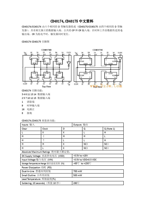
CD40174/CC40174由六个相同的D型触发器组成(CD40175/CC40175由四个相同的D型触发器)。具有相互独立的数据输入端、公共的CP和CR输入端,在时钟上升沿数据传送到Q输出端。CR为低电平时,触发器同时复位。
CD40174 CD40175引脚图
13
35
tH
Time after Clock Pulse that
Data Must be Held
VDD=5V
VDD=10V
-11
0
NS
-4
0
VDD=15V
CD4017中文资料内容说明及其运用

CD4017中文资料内容说明及其运用电子制作2009-11-14 20:09:21 阅读5119 评论1 字号:大中小订阅cd4017中文资料内容说明cd4017中文资料内容说明:CD4017 是5 位Johnson 计数器,具有10 个译码输出端,CP、CR、INH 输入端。
时钟输入端的斯密特触发器具有脉冲整形功能,对输入时钟脉冲上升和下降时间无限制。
INH 为低电平时,计数器在时钟上升沿计数;反之,计数功能无效。
CR 为高电平时,计数器清零。
Johnson 计数器,提供了快速操作、2 输入译码选通和无毛刺译码输出。
防锁选通,保证了正确的计数顺序。
译码输出一般为低电平,只有在对应时钟周期内保持高电平。
在每10 个时钟输入周期CO 信号完成一次进位,并用作多级计数链的下级脉动时钟。
CD4017 提供了16 引线多层陶瓷双列直插(D)、熔封陶瓷双列直插(J)、塑料双列直插(P)和陶瓷片状载体(C)4 种封装形式。
引出端功能符号CO:进位脉冲输渊CP:时钟输入端CR:清除端INH:禁止端Q0-Q9 计数脉冲输出端VDD:正电源VSS:地CD4017组成的防抖动触摸开关电路这是一个实用点触发电路,可以方便的与各种电路组合使用,温度控制,光控,声控,射频遥控。
而只需把这些信号加到CD4017的CP端。
本电路使用一片十进制计数器CD4017,输出Y2和复位端RST相接,14脚每次到两个记数脉冲既复位。
其工作原理是220伏交流电经变压器降压、D1-D4整流、C1滤波后获得+9V直流电压。
C3、R2构成上电复位电路,CD4017复位后Y0输出高电平,Y1和Y2输出低电平,三极管V导通。
继电器吸合,其常开触点接通用电器。
K被按下后,C2迅速放电,14脚获得脉冲上升沿,触发CD4017记数,使Y0输出低电平,Y2仍保持低电平。
此时三极管V截止,继电器释放,用电器断电。
再次按下K时,C2再次放电,14脚又获得一个记数脉冲,CD4017的Y0和Y1输出低电平,Y2输出高电平,通过二极管D5将CD4017复位,Y0 输出高电平,Y1和Y2输出低电平,三极管V再次导通,继电器吸合。
CD40175BD中文资料
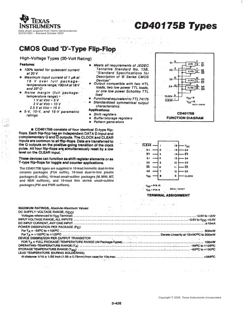
The CD40175B types are supplied in 16-lead hermetic dual-in-line ceramic packages (F3A suffix), 16-lead dual-in-line plastic packages (E suffix), 16-lead small-outline packages (M, M96, MT ,and NSR suffixes), and 16-lead thin shrink small-outline packages (PW and PWR suffixes).Data sheet acquired from Harris Semiconductor SCHS105C − Revised October 2003PACKAGING INFORMATIONOrderable Device Status(1)PackageType PackageDrawingPins PackageQtyEco Plan(2)Lead/Ball Finish MSL Peak Temp(3)CD40175BE ACTIVE PDIP N1625Pb-Free(RoHS)CU NIPDAU N/A for Pkg TypeCD40175BEE4ACTIVE PDIP N1625Pb-Free(RoHS)CU NIPDAU N/A for Pkg Type CD40175BF3A ACTIVE CDIP J161TBD A42SNPB N/A for Pkg Type CD40175BM ACTIVE SOIC D1640Green(RoHS&no Sb/Br)CU NIPDAU Level-1-260C-UNLIMCD40175BM96ACTIVE SOIC D162500Green(RoHS&no Sb/Br)CU NIPDAU Level-1-260C-UNLIMCD40175BM96E4ACTIVE SOIC D162500Green(RoHS&no Sb/Br)CU NIPDAU Level-1-260C-UNLIMCD40175BM96G4ACTIVE SOIC D162500Green(RoHS&no Sb/Br)CU NIPDAU Level-1-260C-UNLIMCD40175BME4ACTIVE SOIC D1640Green(RoHS&no Sb/Br)CU NIPDAU Level-1-260C-UNLIMCD40175BMG4ACTIVE SOIC D1640Green(RoHS&no Sb/Br)CU NIPDAU Level-1-260C-UNLIMCD40175BMT ACTIVE SOIC D16250Green(RoHS&no Sb/Br)CU NIPDAU Level-1-260C-UNLIMCD40175BMTE4ACTIVE SOIC D16250Green(RoHS&no Sb/Br)CU NIPDAU Level-1-260C-UNLIMCD40175BMTG4ACTIVE SOIC D16250Green(RoHS&no Sb/Br)CU NIPDAU Level-1-260C-UNLIMCD40175BNSR ACTIVE SO NS162000Green(RoHS&no Sb/Br)CU NIPDAU Level-1-260C-UNLIMCD40175BNSRE4ACTIVE SO NS162000Green(RoHS&no Sb/Br)CU NIPDAU Level-1-260C-UNLIMCD40175BNSRG4ACTIVE SO NS162000Green(RoHS&no Sb/Br)CU NIPDAU Level-1-260C-UNLIMCD40175BPW ACTIVE TSSOP PW1690Green(RoHS&no Sb/Br)CU NIPDAU Level-1-260C-UNLIMCD40175BPWE4ACTIVE TSSOP PW1690Green(RoHS&no Sb/Br)CU NIPDAU Level-1-260C-UNLIMCD40175BPWG4ACTIVE TSSOP PW1690Green(RoHS&no Sb/Br)CU NIPDAU Level-1-260C-UNLIMCD40175BPWR ACTIVE TSSOP PW162000Green(RoHS&no Sb/Br)CU NIPDAU Level-1-260C-UNLIMCD40175BPWRE4ACTIVE TSSOP PW162000Green(RoHS&no Sb/Br)CU NIPDAU Level-1-260C-UNLIMCD40175BPWRG4ACTIVE TSSOP PW162000Green(RoHS&no Sb/Br)CU NIPDAU Level-1-260C-UNLIMCD40175BW OBSOLETE WAFERSALEYS0TBD Call TI Call TI(1)The marketing status values are defined as follows:ACTIVE:Product device recommended for new designs.LIFEBUY:TI has announced that the device will be discontinued,and a lifetime-buy period is in effect.NRND:Not recommended for new designs.Device is in production to support existing customers,but TI does not recommend using this part in a new design.PREVIEW:Device has been announced but is not in production.Samples may or may not be available.OBSOLETE:TI has discontinued the production of the device.(2)Eco Plan-The planned eco-friendly classification:Pb-Free(RoHS),Pb-Free(RoHS Exempt),or Green(RoHS&no Sb/Br)-please check /productcontent for the latest availability information and additional product content details.TBD:The Pb-Free/Green conversion plan has not been defined.Pb-Free(RoHS):TI's terms"Lead-Free"or"Pb-Free"mean semiconductor products that are compatible with the current RoHS requirements for all6substances,including the requirement that lead not exceed0.1%by weight in homogeneous materials.Where designed to be soldered at high temperatures,TI Pb-Free products are suitable for use in specified lead-free processes.Pb-Free(RoHS Exempt):This component has a RoHS exemption for either1)lead-based flip-chip solder bumps used between the die and package,or2)lead-based die adhesive used between the die and leadframe.The component is otherwise considered Pb-Free(RoHS compatible)as defined above.Green(RoHS&no Sb/Br):TI defines"Green"to mean Pb-Free(RoHS compatible),and free of Bromine(Br)and Antimony(Sb)based flame retardants(Br or Sb do not exceed0.1%by weight in homogeneous material)(3)MSL,Peak Temp.--The Moisture Sensitivity Level rating according to the JEDEC industry standard classifications,and peak solder temperature.Important Information and Disclaimer:The information provided on this page represents TI's knowledge and belief as of the date that it is provided.TI bases its knowledge and belief on information provided by third parties,and makes no representation or warranty as to the accuracy of such information.Efforts are underway to better integrate information from third parties.TI has taken and continues to take reasonable steps to provide representative and accurate information but may not have conducted destructive testing or chemical analysis on incoming materials and chemicals.TI and TI suppliers consider certain information to be proprietary,and thus CAS numbers and other limited information may not be available for release.In no event shall TI's liability arising out of such information exceed the total purchase price of the TI part(s)at issue in this document sold by TI to Customer on an annual basis.TAPE AND REEL INFORMATION*All dimensions are nominalDevicePackage Type Package Drawing Pins SPQReel Diameter (mm)Reel Width W1(mm)A0(mm)B0(mm)K0(mm)P1(mm)W (mm)Pin1Quadrant CD40175BM96SOIC D 162500330.016.4 6.510.3 2.18.016.0Q1CD40175BNSR SO NS 162000330.016.48.210.5 2.512.016.0Q1CD40175BPWRTSSOPPW162000330.012.47.05.61.68.012.0Q1*All dimensions are nominalDevice Package Type Package Drawing Pins SPQ Length(mm)Width(mm)Height(mm) CD40175BM96SOIC D162500333.2345.928.6 CD40175BNSR SO NS162000346.0346.033.0 CD40175BPWR TSSOP PW162000346.0346.029.0IMPORTANT NOTICETexas Instruments Incorporated and its subsidiaries(TI)reserve the right to make corrections,modifications,enhancements,improvements, and other changes to its products and services at any time and to discontinue any product or service without notice.Customers should obtain the latest relevant information before placing orders and should verify that such information is current and complete.All products are sold subject to TI’s terms and conditions of sale supplied at the time of order acknowledgment.TI warrants performance of its hardware products to the specifications applicable at the time of sale in accordance with TI’s standard warranty.Testing and other quality control techniques are used to the extent TI deems necessary to support this warranty.Except where mandated by government requirements,testing of all parameters of each product is not necessarily performed.TI assumes no liability for applications assistance or customer product design.Customers are responsible for their products and applications using TI components.To minimize the risks associated with customer products and applications,customers should provide adequate design and operating safeguards.TI does not warrant or represent that any license,either express or implied,is granted under any TI patent right,copyright,mask work right, or other TI intellectual property right relating to any combination,machine,or process in which TI products or services are rmation published by TI regarding third-party products or services does not constitute a license from TI to use such products or services or a warranty or endorsement e of such information may require a license from a third party under the patents or other intellectual property of the third party,or a license from TI under the patents or other intellectual property of TI.Reproduction of TI information in TI data books or data sheets is permissible only if reproduction is without alteration and is accompanied by all associated warranties,conditions,limitations,and notices.Reproduction of this information with alteration is an unfair and deceptive business practice.TI is not responsible or liable for such altered rmation of third parties may be subject to additional restrictions.Resale of TI products or services with statements different from or beyond the parameters stated by TI for that product or service voids all express and any implied warranties for the associated TI product or service and is an unfair and deceptive business practice.TI is not responsible or liable for any such statements.TI products are not authorized for use in safety-critical applications(such as life support)where a failure of the TI product would reasonably be expected to cause severe personal injury or death,unless officers of the parties have executed an agreement specifically governing such use.Buyers represent that they have all necessary expertise in the safety and regulatory ramifications of their applications,and acknowledge and agree that they are solely responsible for all legal,regulatory and safety-related requirements concerning their products and any use of TI products in such safety-critical applications,notwithstanding any applications-related information or support that may be provided by TI.Further,Buyers must fully indemnify TI and its representatives against any damages arising out of the use of TI products in such safety-critical applications.TI products are neither designed nor intended for use in military/aerospace applications or environments unless the TI products are specifically designated by TI as military-grade or"enhanced plastic."Only products designated by TI as military-grade meet military specifications.Buyers acknowledge and agree that any such use of TI products which TI has not designated as military-grade is solely at the Buyer's risk,and that they are solely responsible for compliance with all legal and regulatory requirements in connection with such use. TI products are neither designed nor intended for use in automotive applications or environments unless the specific TI products are designated by TI as compliant with ISO/TS16949requirements.Buyers acknowledge and agree that,if they use any non-designated products in automotive applications,TI will not be responsible for any failure to meet such requirements.Following are URLs where you can obtain information on other Texas Instruments products and application solutions:Products ApplicationsAmplifiers AudioData Converters AutomotiveDSP BroadbandClocks and Timers Digital ControlInterface MedicalLogic MilitaryPower Mgmt Optical NetworkingMicrocontrollers SecurityRFID TelephonyRF/IF and ZigBee®Solutions Video&ImagingWirelessMailing Address:Texas Instruments,Post Office Box655303,Dallas,Texas75265Copyright©2008,Texas Instruments Incorporated。
CD4017的原理及应用电路

CD4017的原理及应用电路一、原理介绍:CD4017是一种CMOS逻辑芯片,由10位二进制计数器和十个输出引脚组成。
它有一个时钟输入引脚(CLK)和一个复位引脚(RST),CLK触发计数器计数,RST用于将计数器复位为0。
当CLK引脚接收到上升沿时,计数器会递增1,同时输出引脚中的一个将变为高电平,其余输出引脚将变为低电平。
二、工作原理:当CD4017复位后,输出引脚0(Q0)为高电平,其余引脚为低电平。
当CLK输入引脚接收到上升沿时,计数器会递增1、输出引脚中的其中一位(从Q0到Q9)将变为高电平,而上一个高电平输出引脚将变为低电平。
每次计数由上升沿触发,从0到9循环,所以接收到10个时钟脉冲时,所有输出引脚都会被触发一次。
三、应用电路:1.LED跑马灯:CD4017常用于驱动LED的控制电路。
一个简单的应用是LED跑马灯电路。
可以将CD4017与LED灯串联,其中CLK接入一个时钟发生器,RST接入复位开关。
每当接收到一个时钟脉冲时,CD4017会将高电平依次传递给LED灯,使得LED灯按照顺序依次亮起。
2.计数显示器:将CD4017与七段数码管连接,可以构建一个简单的计数显示器。
当接收到时钟脉冲时,CD4017会递增1,并将当前计数值的二进制编码通过输出引脚传递给七段数码管,显示相应的数字。
通过适当的编码和解码电路,可以实现各种不同计数方式的显示。
3.触发摇摆器:4.步进电机控制器:CD4017可以用于步进电机的控制。
通过将CD4017的输出引脚与步进电机控制器的输入引脚连接,可以实现步进电机的顺序控制。
每当接收到时钟脉冲时,CD4017会将高电平输出引脚依次切换,从而控制步进电机的运动方向和步数。
以上是对CD4017的原理与常见应用电路的介绍。
CD4017是一种十分常见的分频计数器,具有较高的性能和稳定性,在各种电子设备中都有广泛的应用。
数字电路CD4017的原理及应用电路

数字电路CD4017的原理及应用电路数字电路CD4017是十进制计数/分频器,它的内部由计数器及译码器两部分组成,由译码输出实现对脉冲信号的分配,整个输出时序就是Q0、Q1、Q2、…、Q9依次出现与时钟同步的高电平,宽度等于时钟周期。
CD4017有10个输出端(Q0~Q9)和1个进位输出端~Q5-9。
每输入10个计数脉冲,~Q5-9就可得到1个进位正脉冲,该进位输出信号可作为下一级的时钟信号。
CD4017有3个输(MR、CP0和~CP1),MR为清零端,当在MR端上加高电平或正脉冲时其输出Q0为高电平,其余输出端(Q1~Q9)均为低电平。
CP0和~CPl是2个时钟输入端,若要用上升沿来计数,则信号由CP0端输入;若要用下降沿来计数,则信号由~CPl端输入。
设置2个时钟输入端,级联时比较方便,可驱动更多二极管发光。
由此可见,当CD4017有连续脉冲输入时,其对应的输出端依次变为高电平状态,故可直接用作顺序脉冲发生器。
CD4017有两个时钟端CP 和EN,若用时钟脉冲的上沿计数,则信号从CP 端输入;若用下降沿计数,则信号从EN 端输入。
设置两个时钟端是为了级联方便。
CD4017 与CD4022 是一对姊妹产品,主要区别是CD4022 是八进制的,所以译码输出仅有Y0~Y7,每输入8 个脉冲周期,就可得到一个进位输出,它们的管脚相同,不过CD4022 的6、9 脚是空脚。
cd4017方框图cd4017引脚图一、用一个CD4017制成的彩灯电路1.用一个CD4017制作的彩灯电路如图1 所示。
cd4017电路图2.电路工作原理CD4017输出高电平的顺序分别是③、②、④、⑦、⑩、①、⑤、⑥、⑨脚,故③、②、④、⑦、⑩、①脚的高电平使6串彩灯向右顺序发光,⑤、⑥、③脚的高电平使6串彩灯由中心向两边散开发光。
各种发光方式可按自己的需要进行具体的组合,若要改变彩灯的闪光速度,可改变电容C1的大小。
二、用三个CD4O17彩灯电路图CD4017的级连,如图2所示。
十进制计数分配器CD4017简介

十进制计数/分配器CD4017简介CD4017是十进制计数/分配器,它有3个输入端,即复位端R、时钟端CP和CP E(也叫EN),CP端为脉冲上升沿有效,CP E为脉冲下降沿有效;它还有10个输出端,即Q0~Q9。
在复位状态时,只有Q0为高电平“1”状态,其它输出端均为低电平“0”状态。
当时钟端输入有效时钟脉冲(CP 端输入上升沿或CP E输入下降沿)时,输出端的高电平在Q0~Q9之间依次循环传递。
CD4017还设有进位输出端CO,当多个CD4017级联使用时该端连接到相邻级的时钟输入端。
CD4017为DIP16脚封装(双列直插封装),各引脚功能见图1,真值表见附表。
这种集成电路在自动控制电路中应用很广泛,是CMOS4000系列数字集成电路中应用率较高的型号之一。
各种报刊介绍的应用电路中经常出现它,本文通过一个实例介绍其应用方法与技巧。
图2所示是一个电子互锁开关电路。
可用于多路信号的切换控制。
图中或非门CD4001的2个门构成键控振荡器,其输出送至CD4017的CP端。
由于振荡器的键控输入端由上拉电阻R1拉至高电平“1”状态,所以在按键SB0~SB9均未按下时振荡器处于停振状态。
十进制计数器CD4017的10个输出端用于控制10个信号通道(这里只画出了控制端口),如果待选信号不足10路,则输出端Q0可空置不用,这样CD4017复位后所有的信号通道均未选中,即接通电源后按一下清零按钮SB,输出端Q0变为高电平,由于Q0端空置,因此没有信号通路被选中。
若欲选中某一路信号,例如受Q5控制的第五路信号,可按下按键SB5,由于按下按键SB5之前Q5端为低电平,所以振荡器的键控端也变为低电平,键控振荡器起振,振荡信号送CD4017的CP端。
因为振荡频率很高(约4.5kHz),在很短时间内(几mS 时间,手还未来得及松开)Q5即由低电平变为高电平,这样受Q5控制的那一路信号即可通过后续电路(未画出)被选中。
同时Q5的高电平反馈到键控端使振荡器停振,Q5的高电平状态被锁定。
CD4017工作原理及应用电路图

CD4017工作原理及应用电路图十进制计数/分频器CD4017,其内部由计数器及译码器两部分组成,由译码输出实现对脉冲信号的分配,整个输出时序就是O0、O1、O2、…、O9依次出现与时钟同步的高电平,宽度等于时钟周期。
CD4017有10个输出端(O0~O9)和1个进位输出端~O5-9。
每输入10个计数脉冲,~O5-9就可得到1个进位正脉冲,该进位输出信号可作为下一级的时钟信号。
CD4017有3个输(MR、CP0和~CP1),MR为清零端,当在MR端上加高电平或正脉冲时其输出O0为高电平,其余输出端(O1~O9)均为低电平。
CP0和~CPl是2个时钟输入端,若要用上升沿来计数,则信号由CP0端输入;若要用下降沿来计数,则信号由~CPl端输入。
设置2个时钟输入端,级联时比较方便,可驱动更多二极管发光。
由此可见,当CD4017有连续脉冲输入时,其对应的输出端依次变为高电平状态,故可直接用作顺序脉冲发生器。
CD4017方框图CD4017引脚图一、用一个CD4017制成的彩灯电路1.用一个CD4017制作的彩灯电路如图1 所示。
CD4017电路图2.电路工作原理CD4017输出高电平的顺序分别是③、②、④、⑦、⑩、①、⑤、⑥、⑨脚,故③、②、④、⑦、⑩、①脚的高电平使6串彩灯向右顺序发光,⑤、⑥、③脚的高电平使6串彩灯由中心向两边散开发光。
各种发光方式可按自己的需要进行具体的组合,若要改变彩灯的闪光速度,可改变电容C1的大小。
二、用三个CD4O17彩灯电路图CD4017的级连,如图2所示。
CD4017原理图电路CD4017级连后可以顺序输出24个高电平,同上理可组合出各种不同的发光方式,见图3,可使6串彩灯向右流水发光,再向左流水发光,中心向两边散开后再向中心靠拢发光,1、3、5、2、4、6串间隔发光等等。
- 1、下载文档前请自行甄别文档内容的完整性,平台不提供额外的编辑、内容补充、找答案等附加服务。
- 2、"仅部分预览"的文档,不可在线预览部分如存在完整性等问题,可反馈申请退款(可完整预览的文档不适用该条件!)。
- 3、如文档侵犯您的权益,请联系客服反馈,我们会尽快为您处理(人工客服工作时间:9:00-18:30)。
40
VDD = 15V
13
35
tH
Time after Clock Pulse that
Data Must be Held
VDD = 5V
−11
0
ns
VDD = 10V
−4
0
VDD = 15V
Байду номын сангаас−3
0
tTHL,tTLH
Transition Time过渡时间
VDD = 5V
100
200
ns
VDD = 10V
7.5
CPD
Power Dissipation功耗
Per Package (Note 6)
130
pF
切换时间波形
0V to VDD VDC
Operating Temperature Range工作温度范围(TA)
−55℃to +125℃
DC Electrical Characteristics直流电气特性:
符号
Parameter参数
Conditions条件
-55℃
25℃
125℃
单位
最小
最大
最小
典型
最大
最小
最大
L
X
X
L
H
H
↑
H
H
L
H
↑
L
L
H
H
H
X
NC
NC
H
L
X
NC
NC
CD40174 CD40175引脚图
CD40174引脚功能:
3 4 6 11 13 14数据输入端
2 5 7 10 12 15数据输入端
1消除端
9时钟输入端
16电源正
8接地
Absolute Maximum Ratings绝对最大额定值:
DC Supply Voltage直流供电电压(VDD)
VDD = 5V
190
300
ns
VDD = 10V
75
110
VDD = 15V
60
90
tPHL
Propagation Delay Time to a
Logical “0” from Clear to Q
VDD = 5V
180
300
ns
VDD = 10V
70
110
VDD = 15V
60
90
tPLH
Propagation Delay Time to a Logical
0.64
0.51
0.88
0.36
mA
VDD = 10V, VO = 0.5V
1.6
1.3
2.25
0.9
VDD = 15V, VO = 1.5V
4.2
3.4
8.8
2.4
IOH
HIGH Level Output Current输出高电平电流
VDD = 5V, VO = 4.6V
−0.64
−0.51
−0.88
50
100
VDD = 15V
40
80
tWH,tWL
Minimum Clock Pulse Width最小时钟脉冲宽度
VDD = 5V
130
250
ns
VDD = 10V
45
100
VDD = 15V
40
80
tWL
Minimum Clear Pulse Width最小无阻脉冲宽度
VDD = 5V
120
250
−0.5V to +18V
Input Voltage输入电压(VIN)
−0.5V to VDD +0.5 VDC
Storage Temperature Range储存温度范围(TS)
−65℃to +150℃
Power Dissipation功耗(PD)
Dual-In-Line普通双列封装
700mW
Small Outline小外形封装
−0.1
10−5
−0.1
1.0
AC Electrical Characteristics交流电气特性:
Symbol符号
Parameter参数
Conditions条件
最小
典型
最大
Units单位
tPHL,tPLH
Propagation Delay Time to a Logical “0” or Logical “1” from Clock to Q or Q (CD40175 Only)
ns
VDD = 10V
45
100
VDD = 15V
40
80
tRCL
Maximum Clock Rise Time最大时钟上升时间
VDD = 5V
15
μs
VDD = 10V
5.0
VDD = 15V
5.0
tfCL
Maximum Clock Fall Time最大时钟下降时间
VDD = 5V
15
50
μs
VDD = 10V
VDD=5V,VO =0.5V or 4.5V
3.5
3.5
3.5
V
VDD=10V,VO=1V or 9V
7.0
7.0
7.0
VDD=15V,VO=1.5V or 13.5V
11.0
11.0
11.0
IOL
LOW Level Output Current输出低电平电流
VDD = 5V, VO = 0.4V
500mW
Lead Temperature焊接温度(TL)
Soldering, 10 seconds)(焊接10秒)
260℃
Recommended Operating Conditions建议操作条件:
DC Supply Voltage直流供电电压(VDD)
3V to 15 VDC
Input Voltage输入电压(VIN)
5.0
50
VDD = 15V
5.0
50
fCL
Maximum Clock Frequency最大时钟频率
VDD = 5V
2.0
3.5
MHz
VDD = 10V
5.0
10
VDD = 15V
6.0
12
CIN
Input Capacitance输入电容
Clear Input
10
15
pF
Other Input
5.0
VDD=5V
|IO|<1μA
0.05
0.05
0.05
V
VDD=10V
0.05
0.05
0.05
VDD=15V
0.05
0.05
0.05
VOH
HIGH Level Output Voltage输出高电平电压
VDD=5V
|IO|<1μA
4.95
4.95
5
4.95
V
VDD=10V
9.95
9.95
10
9.95
VDD=15V
14.95
14.95
15
14.95
VIL
LOW Level Input Voltage输入低电平电压
VDD=5V,VO=0.5Vor4.5V
1.5
1.5
1.5
V
VDD=10V, VO = 1V or 9V
3.0
3.0
3.0
VDD=15V,VO=1.5V or 13.5V
4.0
4.0
4.0
VIH
HIGH Level Input Voltage输入高电平电压
“1” from Clear to Q (CD40175 Only)
VDD = 5V
230
400
ns
VDD = 10V
90
150
VDD = 15V
75
120
tSU
Time Prior to Clock Pulse that
Data must be Present
VDD = 5V
45
100
ns
VDD = 10V
−0.36
mA
VDD = 10V, VO = 9.5V
−1.6
−1.3
−2.25
−0.9
VDD = 15V, VO = 13.5V
−4.2
−3.4
−8.8
−2.4
IIN
Input Current输入电流
VDD=15V,VIN = 0V
0.1
−10−5
0.1
−1.0
μA
VDD=15V,VIN = 15V
CD40174/CC40174由六个相同的D型触发器组成(CD40175/CC40175由四个相同的D型触发器)。具有相互独立的数据输入端、公共的CP和CR输入端,在时钟上升沿数据传送到Q输出端。CR为低电平时,触发器同时复位。
真值表功能:
Inputs输入
Outputs输出
Clear
Clock
D
Q
Q(Note 1)
IDD
Quiescent Device Current静态电流
VDD=5V,VIN = VDD or VSS
1.0
1.0
30
μA
VDD=10V,VIN = VDD or VSS
2.0
2.0
60
VDD=15V,VIN = VDD or VSS