2AC6;中文规格书,Datasheet资料
9906;中文规格书,Datasheet资料
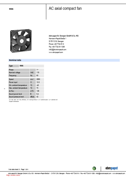
Nominal data
Type Phase Nominal voltage Frequency Speed Power input Min. ambient temperature Max. ambient temperature Air flow Sound power level Sound pressure level VAC Hz min-1 W °C °C m3/h B dB(A) 9906 1~ 115 60 2850 12.0 -40 70 135 5.4 42
/
9906
AC axial compact fan
Technical features
General description AC voltage fan with internal rotor shaded-pole motor. Protected from overload by impedance protection. Fan housing made of metal, impeller made of mineral-reinforced PA plastic. Air exhaust over bars. Direction of rotation counter-clockwise seen on rotor. Electrical connection to 2 flat plugs 2.8 x 0.5 mm. Fan housing with grounding lug for M4 tapping screw. Mass 320 g. Please note our new ACmaxx series. With identical fastening dimensions and voltages, this series achieves higher energy efficiency. 0.325 kg 119 x 119 x 25 mm Mineral-reinforced PA plastic Metal Air exhaust over bars Left, looking at rotor Ball bearings 52500 h 25000 h 2 flat plugs 2.8 x 0.5 mm Protected from overload using impedance protection VDE, CSA, UL, CE
TL082ACDR,TL082ACDR,TL082ACDR,TL082IDR,TL082IDR,TL082IDR,TL081CDR,TL081CDR, 规格书,Datasheet 资料

Addendum-Page 1PACKAGING INFORMATIONOrderable Device Status(1)Package Type PackageDrawingPins Package QtyEco Plan(2)Lead/Ball Finish MSL Peak Temp (3)Samples (Requires Login)5962-9851501Q2A ACTIVE LCCC FK 201TBD Call TI Call TI5962-9851501QPA ACTIVE CDIP JG 81TBD A42N / A for Pkg Type 5962-9851503Q2A ACTIVE LCCC FK 201TBD Call TI Call TI 5962-9851503QCAACTIVE CDIP J 141TBDCall TICall TITL081ACD ACTIVE SOIC D 875Green (RoHS & no Sb/Br)CU NIPDAU Level-1-260C-UNLIM TL081ACDE4ACTIVE SOIC D 875Green (RoHS & no Sb/Br)CU NIPDAU Level-1-260C-UNLIM TL081ACDG4ACTIVE SOIC D 875Green (RoHS & no Sb/Br)CU NIPDAU Level-1-260C-UNLIM TL081ACDR ACTIVE SOIC D 82500Green (RoHS & no Sb/Br)CU NIPDAU Level-1-260C-UNLIM TL081ACDRE4ACTIVE SOIC D 82500Green (RoHS & no Sb/Br)CU NIPDAU Level-1-260C-UNLIM TL081ACDRG4ACTIVE SOIC D 82500Green (RoHS & no Sb/Br)CU NIPDAU Level-1-260C-UNLIM TL081ACJG OBSOLETE CDIP JG 8TBD Call TICall TITL081ACP ACTIVE PDIP P 850Pb-Free (RoHS)CU NIPDAU N / A for Pkg Type TL081ACPE4ACTIVE PDIP P 850Pb-Free (RoHS)CU NIPDAU N / A for Pkg Type TL081BCD ACTIVE SOIC D 875Green (RoHS & no Sb/Br)CU NIPDAU Level-1-260C-UNLIM TL081BCDE4ACTIVE SOIC D 875Green (RoHS & no Sb/Br)CU NIPDAU Level-1-260C-UNLIM TL081BCDG4ACTIVE SOIC D 875Green (RoHS & no Sb/Br)CU NIPDAU Level-1-260C-UNLIM TL081BCDR ACTIVE SOIC D 82500Green (RoHS & no Sb/Br)CU NIPDAU Level-1-260C-UNLIM TL081BCDRE4ACTIVE SOIC D 82500Green (RoHS & no Sb/Br)CU NIPDAU Level-1-260C-UNLIM TL081BCDRG4ACTIVE SOIC D 82500Green (RoHS & no Sb/Br)CU NIPDAU Level-1-260C-UNLIM TL081BCP ACTIVE PDIP P 850Pb-Free (RoHS)CU NIPDAU N / A for Pkg Type TL081BCPE4ACTIVEPDIPP850Pb-Free (RoHS)CU NIPDAU N / A for Pkg Type芯天下--/Addendum-Page 2Orderable DeviceStatus(1)Package Type PackageDrawingPins Package QtyEco Plan(2)Lead/Ball FinishMSL Peak Temp(3)Samples (Requires Login)TL081CD ACTIVE SOIC D 875Green (RoHS & no Sb/Br)CU NIPDAU Level-1-260C-UNLIM TL081CDE4ACTIVE SOIC D 875Green (RoHS & no Sb/Br)CU NIPDAU Level-1-260C-UNLIM TL081CDG4ACTIVE SOIC D 875Green (RoHS & no Sb/Br)CU NIPDAU Level-1-260C-UNLIM TL081CDR ACTIVE SOIC D 82500Green (RoHS & no Sb/Br)CU NIPDAU Level-1-260C-UNLIM TL081CDRE4ACTIVE SOIC D 82500Green (RoHS & no Sb/Br)CU NIPDAU Level-1-260C-UNLIM TL081CDRG4ACTIVE SOIC D 82500Green (RoHS & no Sb/Br)CU NIPDAU Level-1-260C-UNLIM TL081CP ACTIVE PDIP P 850Pb-Free (RoHS)CU NIPDAU N / A for Pkg Type TL081CPE4ACTIVE PDIP P 850Pb-Free (RoHS)CU NIPDAU N / A for Pkg Type TL081CPSR ACTIVE SO PS 82000Green (RoHS & no Sb/Br)CU NIPDAU Level-1-260C-UNLIM TL081CPSRE4ACTIVE SO PS 82000Green (RoHS & no Sb/Br)CU NIPDAU Level-1-260C-UNLIM TL081CPSRG4ACTIVE SO PS 82000Green (RoHS & no Sb/Br)CU NIPDAU Level-1-260C-UNLIM TL081CPWLE OBSOLETE TSSOP PW 8TBD Call TICall TITL081ID ACTIVE SOIC D 875Green (RoHS & no Sb/Br)CU NIPDAU Level-1-260C-UNLIM TL081IDE4ACTIVE SOIC D 875Green (RoHS & no Sb/Br)CU NIPDAU Level-1-260C-UNLIM TL081IDG4ACTIVE SOIC D 875Green (RoHS & no Sb/Br)CU NIPDAU Level-1-260C-UNLIM TL081IDR ACTIVE SOIC D 82500Green (RoHS & no Sb/Br)CU NIPDAU Level-1-260C-UNLIM TL081IDRE4ACTIVE SOIC D 82500Green (RoHS & no Sb/Br)CU NIPDAU Level-1-260C-UNLIM TL081IDRG4ACTIVE SOIC D 82500Green (RoHS & no Sb/Br)CU NIPDAU Level-1-260C-UNLIM TL081IP ACTIVE PDIP P 850Pb-Free (RoHS)CU NIPDAU N / A for Pkg Type TL081IPE4ACTIVEPDIPP850Pb-Free (RoHS)CU NIPDAU N / A for Pkg Type芯天下--/Addendum-Page 3Orderable Device Status(1)Package Type PackageDrawingPins Package QtyEco Plan(2)Lead/Ball Finish MSL Peak Temp (3)Samples (Requires Login)TL081MFKB OBSOLETE LCCC FK 20TBD Call TI Call TI TL081MJG OBSOLETE CDIP JG 8TBD Call TI Call TI TL081MJGB OBSOLETE CDIP JG 8TBDCall TICall TITL082ACD ACTIVE SOIC D 875Green (RoHS & no Sb/Br)CU NIPDAU Level-1-260C-UNLIM TL082ACDE4ACTIVE SOIC D 875Green (RoHS & no Sb/Br)CU NIPDAU Level-1-260C-UNLIM TL082ACDG4ACTIVE SOIC D 875Green (RoHS & no Sb/Br)CU NIPDAU Level-1-260C-UNLIM TL082ACDR ACTIVE SOIC D 82500Green (RoHS & no Sb/Br)CU NIPDAU Level-1-260C-UNLIM TL082ACDRE4ACTIVE SOIC D 82500Green (RoHS & no Sb/Br)CU NIPDAU Level-1-260C-UNLIM TL082ACDRG4ACTIVE SOIC D 82500Green (RoHS & no Sb/Br)CU NIPDAU Level-1-260C-UNLIM TL082ACP ACTIVE PDIP P 850Pb-Free (RoHS)CU NIPDAU N / A for Pkg Type TL082ACPE4ACTIVE PDIP P 850Pb-Free (RoHS)CU NIPDAU N / A for Pkg Type TL082ACPSR ACTIVE SO PS 82000Green (RoHS & no Sb/Br)CU NIPDAU Level-1-260C-UNLIM TL082ACPSRE4ACTIVE SO PS 82000Green (RoHS & no Sb/Br)CU NIPDAU Level-1-260C-UNLIM TL082ACPSRG4ACTIVE SO PS 82000Green (RoHS & no Sb/Br)CU NIPDAU Level-1-260C-UNLIM TL082BCD ACTIVE SOIC D 875Green (RoHS & no Sb/Br)CU NIPDAU Level-1-260C-UNLIM TL082BCDE4ACTIVE SOIC D 875Green (RoHS & no Sb/Br)CU NIPDAU Level-1-260C-UNLIM TL082BCDG4ACTIVE SOIC D 875Green (RoHS & no Sb/Br)CU NIPDAU Level-1-260C-UNLIM TL082BCDR ACTIVE SOIC D 82500Green (RoHS & no Sb/Br)CU NIPDAU Level-1-260C-UNLIM TL082BCDRE4ACTIVE SOIC D 82500Green (RoHS & no Sb/Br)CU NIPDAU Level-1-260C-UNLIM TL082BCDRG4ACTIVESOICD82500Green (RoHS & no Sb/Br)CU NIPDAU Level-1-260C-UNLIM芯天下--/Addendum-Page 4Orderable DeviceStatus(1)Package Type PackageDrawingPins Package QtyEco Plan(2)Lead/Ball FinishMSL Peak Temp(3)Samples (Requires Login)TL082BCP ACTIVE PDIP P 850Pb-Free (RoHS)CU NIPDAU N / A for Pkg Type TL082BCPE4ACTIVE PDIP P 850Pb-Free (RoHS)CU NIPDAU N / A for Pkg Type TL082CD ACTIVE SOIC D 875Green (RoHS & no Sb/Br)CU NIPDAU Level-1-260C-UNLIM TL082CDE4ACTIVE SOIC D 875Green (RoHS & no Sb/Br)CU NIPDAU Level-1-260C-UNLIM TL082CDG4ACTIVE SOIC D 875Green (RoHS & no Sb/Br)CU NIPDAU Level-1-260C-UNLIM TL082CDR ACTIVE SOIC D 82500Green (RoHS & no Sb/Br)CU NIPDAU Level-1-260C-UNLIM TL082CDRE4ACTIVE SOIC D 82500Green (RoHS & no Sb/Br)CU NIPDAU Level-1-260C-UNLIM TL082CDRG4ACTIVE SOIC D 82500Green (RoHS & no Sb/Br)CU NIPDAU Level-1-260C-UNLIM TL082CJG OBSOLETE CDIP JG 8TBD Call TICall TITL082CP ACTIVE PDIP P 850Pb-Free (RoHS)CU NIPDAU N / A for Pkg Type TL082CPE4ACTIVE PDIP P 850Pb-Free (RoHS)CU NIPDAU N / A for Pkg Type TL082CPSR ACTIVE SO PS 82000Green (RoHS & no Sb/Br)CU NIPDAU Level-1-260C-UNLIM TL082CPSRG4ACTIVE SO PS 82000Green (RoHS & no Sb/Br)CU NIPDAU Level-1-260C-UNLIM TL082CPW ACTIVE TSSOP PW 8150Green (RoHS & no Sb/Br)CU NIPDAU Level-1-260C-UNLIM TL082CPWE4ACTIVE TSSOP PW 8150Green (RoHS & no Sb/Br)CU NIPDAU Level-1-260C-UNLIM TL082CPWG4ACTIVE TSSOP PW 8150Green (RoHS & no Sb/Br)CU NIPDAU Level-1-260C-UNLIM TL082CPWLE OBSOLETE TSSOP PW 8TBD Call TICall TITL082CPWR ACTIVE TSSOP PW 82000Green (RoHS & no Sb/Br)CU NIPDAU Level-1-260C-UNLIM TL082CPWRE4ACTIVE TSSOP PW 82000Green (RoHS & no Sb/Br)CU NIPDAU Level-1-260C-UNLIM TL082CPWRG4ACTIVETSSOPPW82000Green (RoHS & no Sb/Br)CU NIPDAU Level-1-260C-UNLIM芯天下--/27-Apr-2012Orderable Device Status (1)Package Type PackageDrawing Pins Package Qty Eco Plan (2)Lead/Ball FinishMSL Peak Temp (3)Samples(Requires Login)TL082ID ACTIVE SOIC D875Green (RoHS& no Sb/Br)CU NIPDAU Level-1-260C-UNLIMTL082IDE4ACTIVE SOIC D875Green (RoHS& no Sb/Br)CU NIPDAU Level-1-260C-UNLIMTL082IDG4ACTIVE SOIC D875Green (RoHS& no Sb/Br)CU NIPDAU Level-1-260C-UNLIMTL082IDR ACTIVE SOIC D82500Green (RoHS& no Sb/Br)CU NIPDAU Level-1-260C-UNLIMTL082IDRE4ACTIVE SOIC D82500Green (RoHS& no Sb/Br)CU NIPDAU Level-1-260C-UNLIMTL082IDRG4ACTIVE SOIC D82500Green (RoHS& no Sb/Br)CU NIPDAU Level-1-260C-UNLIM TL082IJG OBSOLETE CDIP JG8TBD Call TI Call TITL082IP ACTIVE PDIP P850Pb-Free (RoHS)CU NIPDAU N / A for Pkg Type TL082IPE4ACTIVE PDIP P850Pb-Free (RoHS)CU NIPDAU N / A for Pkg Type TL082IPWR ACTIVE TSSOP PW82000Green (RoHS& no Sb/Br)CU NIPDAU Level-1-260C-UNLIMTL082IPWRE4ACTIVE TSSOP PW82000Green (RoHS& no Sb/Br)CU NIPDAU Level-1-260C-UNLIMTL082IPWRG4ACTIVE TSSOP PW82000Green (RoHS& no Sb/Br)CU NIPDAU Level-1-260C-UNLIM TL082MFK OBSOLETE LCCC FK20TBD Call TI Call TITL082MFKB ACTIVE LCCC FK201TBD POST-PLATE N / A for Pkg Type TL082MJG ACTIVE CDIP JG81TBD A42N / A for Pkg Type TL082MJGB ACTIVE CDIP JG81TBD A42N / A for Pkg Type TL084ACD ACTIVE SOIC D1450Green (RoHS& no Sb/Br)CU NIPDAU Level-1-260C-UNLIMTL084ACDE4ACTIVE SOIC D1450Green (RoHS& no Sb/Br)CU NIPDAU Level-1-260C-UNLIMTL084ACDG4ACTIVE SOIC D1450Green (RoHS& no Sb/Br)CU NIPDAU Level-1-260C-UNLIMTL084ACDR ACTIVE SOIC D142500Green (RoHS& no Sb/Br)CU NIPDAU Level-1-260C-UNLIMTL084ACDRE4ACTIVE SOIC D142500Green (RoHS& no Sb/Br)CU NIPDAU Level-1-260C-UNLIM27-Apr-2012Orderable Device Status (1)Package Type PackageDrawing Pins Package Qty Eco Plan (2)Lead/Ball FinishMSL Peak Temp (3)Samples(Requires Login)TL084ACDRG4ACTIVE SOIC D142500Green (RoHS& no Sb/Br)CU NIPDAU Level-1-260C-UNLIMTL084ACN ACTIVE PDIP N1425Pb-Free (RoHS)CU NIPDAU N / A for Pkg Type TL084ACNE4ACTIVE PDIP N1425Pb-Free (RoHS)CU NIPDAU N / A for Pkg Type TL084ACNSR ACTIVE SO NS142000Green (RoHS& no Sb/Br)CU NIPDAU Level-1-260C-UNLIMTL084ACNSRE4ACTIVE SO NS142000Green (RoHS& no Sb/Br)CU NIPDAU Level-1-260C-UNLIMTL084ACNSRG4ACTIVE SO NS142000Green (RoHS& no Sb/Br)CU NIPDAU Level-1-260C-UNLIMTL084BCD ACTIVE SOIC D1450Green (RoHS& no Sb/Br)CU NIPDAU Level-1-260C-UNLIMTL084BCDE4ACTIVE SOIC D1450Green (RoHS& no Sb/Br)CU NIPDAU Level-1-260C-UNLIMTL084BCDG4ACTIVE SOIC D1450Green (RoHS& no Sb/Br)CU NIPDAU Level-1-260C-UNLIMTL084BCDR ACTIVE SOIC D142500Green (RoHS& no Sb/Br)CU NIPDAU Level-1-260C-UNLIMTL084BCDRE4ACTIVE SOIC D142500Green (RoHS& no Sb/Br)CU NIPDAU Level-1-260C-UNLIMTL084BCDRG4ACTIVE SOIC D142500Green (RoHS& no Sb/Br)CU NIPDAU Level-1-260C-UNLIM TL084BCN ACTIVE PDIP N1425Pb-Free (RoHS)CU NIPDAU N / A for Pkg Type TL084BCNE4ACTIVE PDIP N1425Pb-Free (RoHS)CU NIPDAU N / A for Pkg Type TL084CD ACTIVE SOIC D1450Green (RoHS& no Sb/Br)CU NIPDAU Level-1-260C-UNLIMTL084CDE4ACTIVE SOIC D1450Green (RoHS& no Sb/Br)CU NIPDAU Level-1-260C-UNLIMTL084CDG4ACTIVE SOIC D1450Green (RoHS& no Sb/Br)CU NIPDAU Level-1-260C-UNLIMTL084CDR ACTIVE SOIC D142500Green (RoHS& no Sb/Br)CU NIPDAU Level-1-260C-UNLIMTL084CDRE4ACTIVE SOIC D142500Green (RoHS& no Sb/Br)CU NIPDAU Level-1-260C-UNLIM27-Apr-2012Orderable Device Status (1)Package Type PackageDrawing Pins Package Qty Eco Plan (2)Lead/Ball FinishMSL Peak Temp (3)Samples(Requires Login)TL084CDRG4ACTIVE SOIC D142500Green (RoHS& no Sb/Br)CU NIPDAU Level-1-260C-UNLIMTL084CJ OBSOLETE CDIP J14TBD Call TI Call TITL084CN ACTIVE PDIP N1425Pb-Free (RoHS)CU NIPDAU N / A for Pkg Type TL084CNE4ACTIVE PDIP N1425Pb-Free (RoHS)CU NIPDAU N / A for Pkg Type TL084CNSLE OBSOLETE SO NS14TBD Call TI Call TITL084CNSR ACTIVE SO NS142000Green (RoHS& no Sb/Br)CU NIPDAU Level-1-260C-UNLIMTL084CNSRG4ACTIVE SO NS142000Green (RoHS& no Sb/Br)CU NIPDAU Level-1-260C-UNLIMTL084CPW ACTIVE TSSOP PW1490Green (RoHS& no Sb/Br)CU NIPDAU Level-1-260C-UNLIMTL084CPWE4ACTIVE TSSOP PW1490Green (RoHS& no Sb/Br)CU NIPDAU Level-1-260C-UNLIMTL084CPWG4ACTIVE TSSOP PW1490Green (RoHS& no Sb/Br)CU NIPDAU Level-1-260C-UNLIM TL084CPWLE OBSOLETE TSSOP PW14TBD Call TI Call TITL084CPWR ACTIVE TSSOP PW142000Green (RoHS& no Sb/Br)CU NIPDAU Level-1-260C-UNLIMTL084CPWRE4ACTIVE TSSOP PW142000Green (RoHS& no Sb/Br)CU NIPDAU Level-1-260C-UNLIMTL084CPWRG4ACTIVE TSSOP PW142000Green (RoHS& no Sb/Br)CU NIPDAU Level-1-260C-UNLIMTL084ID ACTIVE SOIC D1450Green (RoHS& no Sb/Br)CU NIPDAU Level-1-260C-UNLIMTL084IDE4ACTIVE SOIC D1450Green (RoHS& no Sb/Br)CU NIPDAU Level-1-260C-UNLIMTL084IDG4ACTIVE SOIC D1450Green (RoHS& no Sb/Br)CU NIPDAU Level-1-260C-UNLIMTL084IDR ACTIVE SOIC D142500Green (RoHS& no Sb/Br)CU NIPDAU Level-1-260C-UNLIMTL084IDRE4ACTIVE SOIC D142500Green (RoHS& no Sb/Br)CU NIPDAU Level-1-260C-UNLIMTL084IDRG4ACTIVE SOIC D142500Green (RoHS& no Sb/Br)CU NIPDAU Level-1-260C-UNLIM27-Apr-2012Orderable Device Status (1)Package Type PackageDrawing Pins Package Qty Eco Plan (2)Lead/Ball FinishMSL Peak Temp (3)Samples(Requires Login)TL084IJ OBSOLETE CDIP J14TBD Call TI Call TITL084IN ACTIVE PDIP N1425Pb-Free (RoHS)CU NIPDAU N / A for Pkg TypeTL084INE4ACTIVE PDIP N1425Pb-Free (RoHS)CU NIPDAU N / A for Pkg TypeTL084MFK ACTIVE LCCC FK201TBD POST-PLATE N / A for Pkg TypeTL084MFKB ACTIVE LCCC FK201TBD POST-PLATE N / A for Pkg TypeTL084MJ ACTIVE CDIP J141TBD A42N / A for Pkg TypeTL084MJB ACTIVE CDIP J141TBD A42N / A for Pkg TypeTL084QD ACTIVE SOIC D1450Green (RoHS& no Sb/Br)CU NIPDAU Level-1-260C-UNLIMTL084QDG4ACTIVE SOIC D1450Green (RoHS& no Sb/Br)CU NIPDAU Level-1-260C-UNLIMTL084QDR ACTIVE SOIC D142500Green (RoHS& no Sb/Br)CU NIPDAU Level-1-260C-UNLIMTL084QDRG4ACTIVE SOIC D142500Green (RoHS& no Sb/Br)CU NIPDAU Level-1-260C-UNLIM(1) The marketing status values are defined as follows:ACTIVE: Product device recommended for new designs.LIFEBUY: TI has announced that the device will be discontinued, and a lifetime-buy period is in effect.NRND: Not recommended for new designs. Device is in production to support existing customers, but TI does not recommend using this part in a new design.PREVIEW: Device has been announced but is not in production. Samples may or may not be available.OBSOLETE: TI has discontinued the production of the device.(2) Eco Plan - The planned eco-friendly classification: Pb-Free (RoHS), Pb-Free (RoHS Exempt), or Green (RoHS & no Sb/Br) - please check /productcontent for the latest availability information and additional product content details.TBD: The Pb-Free/Green conversion plan has not been defined.Pb-Free (RoHS): TI's terms "Lead-Free" or "Pb-Free" mean semiconductor products that are compatible with the current RoHS requirements for all 6 substances, including the requirement that lead not exceed 0.1% by weight in homogeneous materials. Where designed to be soldered at high temperatures, TI Pb-Free products are suitable for use in specified lead-free processes.Pb-Free (RoHS Exempt): This component has a RoHS exemption for either 1) lead-based flip-chip solder bumps used between the die and package, or 2) lead-based die adhesive used between the die and leadframe. The component is otherwise considered Pb-Free (RoHS compatible) as defined above.Green (RoHS & no Sb/Br): TI defines "Green" to mean Pb-Free (RoHS compatible), and free of Bromine (Br) and Antimony (Sb) based flame retardants (Br or Sb do not exceed 0.1% by weight in homogeneous material)(3) MSL, Peak Temp. -- The Moisture Sensitivity Level rating according to the JEDEC industry standard classifications, and peak solder temperature.Important Information and Disclaimer:The information provided on this page represents TI's knowledge and belief as of the date that it is provided. TI bases its knowledge and belief on information provided by third parties, and makes no representation or warranty as to the accuracy of such information. Efforts are underway to better integrate information from third parties. TI has taken and27-Apr-2012 continues to take reasonable steps to provide representative and accurate information but may not have conducted destructive testing or chemical analysis on incoming materials and chemicals. TI and TI suppliers consider certain information to be proprietary, and thus CAS numbers and other limited information may not be available for release.In no event shall TI's liability arising out of such information exceed the total purchase price of the TI part(s) at issue in this document sold by TI to Customer on an annual basis.OTHER QUALIFIED VERSIONS OF TL082, TL082M, TL084, TL084M :•Catalog: TL082, TL084•Automotive: TL082-Q1, TL082-Q1•Military: TL082M, TL084MNOTE: Qualified Version Definitions:•Catalog - TI's standard catalog product•Automotive - Q100 devices qualified for high-reliability automotive applications targeting zero defects•Military - QML certified for Military and Defense ApplicationsTAPE AND REELINFORMATION*Alldimensions are nominalDevicePackage Type Package Drawing Pins SPQReel Diameter (mm)Reel Width W1(mm)A0(mm)B0(mm)K0(mm)P1(mm)W (mm)Pin1Quadrant TL081ACDR SOIC D 82500330.012.4 6.4 5.2 2.18.012.0Q1TL081BCDR SOIC D 82500330.012.4 6.4 5.2 2.18.012.0Q1TL081CDR SOIC D 82500330.012.4 6.4 5.2 2.18.012.0Q1TL081CPSR SO PS 82000330.016.48.2 6.6 2.512.016.0Q1TL081IDR SOIC D 82500330.012.4 6.4 5.2 2.18.012.0Q1TL082ACDR SOIC D 82500330.012.4 6.4 5.2 2.18.012.0Q1TL082ACDR SOIC D 82500330.012.4 6.4 5.2 2.18.012.0Q1TL082ACPSR SO PS 82000330.016.48.2 6.6 2.512.016.0Q1TL082BCDR SOIC D 82500330.012.4 6.4 5.2 2.18.012.0Q1TL082CDR SOIC D 82500330.012.4 6.4 5.2 2.18.012.0Q1TL082CDR SOIC D 82500330.012.4 6.4 5.2 2.18.012.0Q1TL082CPSR SO PS 82000330.016.48.2 6.6 2.512.016.0Q1TL082CPWR TSSOP PW 82000330.012.47.0 3.6 1.68.012.0Q1TL082IDR SOIC D 82500330.012.4 6.4 5.2 2.18.012.0Q1TL082IDR SOIC D 82500330.012.4 6.4 5.2 2.18.012.0Q1TL082IPWR TSSOP PW 82000330.012.47.0 3.6 1.68.012.0Q1TL084ACDR SOIC D 142500330.016.4 6.59.0 2.18.016.0Q1TL084ACDRSOICD142500330.016.46.59.02.18.016.0Q114-Jul-2012DevicePackage Type Package Drawing Pins SPQReel Diameter (mm)Reel Width W1(mm)A0(mm)B0(mm)K0(mm)P1(mm)W (mm)Pin1Quadrant TL084ACNSR SO NS 142000330.016.48.210.5 2.512.016.0Q1TL084BCDR SOIC D 142500330.016.4 6.59.0 2.18.016.0Q1TL084CDR SOIC D 142500330.016.4 6.59.0 2.18.016.0Q1TL084CNSR SO NS 142000330.016.48.210.5 2.512.016.0Q1TL084CPWR TSSOP PW 142000330.012.4 6.9 5.6 1.68.012.0Q1TL084IDR SOIC D 142500330.016.4 6.59.0 2.18.016.0Q1TL084QDRSOICD142500330.016.46.59.02.18.016.0Q1*All dimensions are nominalDevice Package TypePackage DrawingPins SPQ Length (mm)Width (mm)Height (mm)TL081ACDR SOIC D 82500340.5338.120.6TL081BCDR SOIC D 82500340.5338.120.6TL081CDR SOIC D 82500340.5338.120.6TL081CPSR SO PS 82000367.0367.038.0TL081IDR SOIC D 82500340.5338.120.6TL082ACDR SOIC D 82500340.5338.120.6TL082ACDR SOIC D 82500367.0367.035.0TL082ACPSR SO PS 82000367.0367.038.0TL082BCDR SOIC D 82500340.5338.120.6TL082CDRSOICD82500340.5338.120.614-Jul-2012Device PackageTypePackage DrawingPins SPQ Length (mm)Width (mm)Height (mm)TL082CDR SOIC D 82500367.0367.035.0TL082CPSR SO PS 82000367.0367.038.0TL082CPWR TSSOP PW 82000367.0367.035.0TL082IDR SOIC D 82500367.0367.035.0TL082IDR SOIC D 82500340.5338.120.6TL082IPWR TSSOP PW 82000367.0367.035.0TL084ACDR SOIC D 142500333.2345.928.6TL084ACDR SOIC D 142500367.0367.038.0TL084ACNSR SO NS 142000367.0367.038.0TL084BCDR SOIC D 142500333.2345.928.6TL084CDR SOIC D 142500333.2345.928.6TL084CNSR SO NS 142000367.0367.038.0TL084CPWR TSSOP PW 142000367.0367.035.0TL084IDR SOIC D 142500333.2345.928.6TL084QDRSOICD142500367.0367.038.014-Jul-2012IMPORTANT NOTICETexas Instruments Incorporated and its subsidiaries(TI)reserve the right to make corrections,enhancements,improvements and other changes to its semiconductor products and services per JESD46C and to discontinue any product or service per JESD48B.Buyers should obtain the latest relevant information before placing orders and should verify that such information is current and complete.All semiconductor products(also referred to herein as“components”)are sold subject to TI’s terms and conditions of sale supplied at the time of order acknowledgment.TI warrants performance of its components to the specifications applicable at the time of sale,in accordance with the warranty in TI’s terms and conditions of sale of semiconductor products.Testing and other quality control techniques are used to the extent TI deems necessary to support this warranty.Except where mandated by applicable law,testing of all parameters of each component is not necessarily performed.TI assumes no liability for applications assistance or the design of Buyers’products.Buyers are responsible for their products and applications using TI components.To minimize the risks associated with Buyers’products and applications,Buyers should provide adequate design and operating safeguards.TI does not warrant or represent that any license,either express or implied,is granted under any patent right,copyright,mask work right,or other intellectual property right relating to any combination,machine,or process in which TI components or services are rmation published by TI regarding third-party products or services does not constitute a license to use such products or services or a warranty or endorsement e of such information may require a license from a third party under the patents or other intellectual property of the third party,or a license from TI under the patents or other intellectual property of TI.Reproduction of significant portions of TI information in TI data books or data sheets is permissible only if reproduction is without alteration and is accompanied by all associated warranties,conditions,limitations,and notices.TI is not responsible or liable for such altered rmation of third parties may be subject to additional restrictions.Resale of TI components or services with statements different from or beyond the parameters stated by TI for that component or service voids all express and any implied warranties for the associated TI component or service and is an unfair and deceptive business practice. TI is not responsible or liable for any such statements.Buyer acknowledges and agrees that it is solely responsible for compliance with all legal,regulatory and safety-related requirements concerning its products,and any use of TI components in its applications,notwithstanding any applications-related information or support that may be provided by TI.Buyer represents and agrees that it has all the necessary expertise to create and implement safeguards which anticipate dangerous consequences of failures,monitor failures and their consequences,lessen the likelihood of failures that might cause harm and take appropriate remedial actions.Buyer will fully indemnify TI and its representatives against any damages arising out of the use of any TI components in safety-critical applications.In some cases,TI components may be promoted specifically to facilitate safety-related applications.With such components,TI’s goal is to help enable customers to design and create their own end-product solutions that meet applicable functional safety standards and requirements.Nonetheless,such components are subject to these terms.No TI components are authorized for use in FDA Class III(or similar life-critical medical equipment)unless authorized officers of the parties have executed a special agreement specifically governing such use.Only those TI components which TI has specifically designated as military grade or“enhanced plastic”are designed and intended for use in military/aerospace applications or environments.Buyer acknowledges and agrees that any military or aerospace use of TI components which have not been so designated is solely at the Buyer's risk,and that Buyer is solely responsible for compliance with all legal and regulatory requirements in connection with such use.TI has specifically designated certain components which meet ISO/TS16949requirements,mainly for automotive ponents which have not been so designated are neither designed nor intended for automotive use;and TI will not be responsible for any failure of such components to meet such requirements.Products ApplicationsAudio /audio Automotive and Transportation /automotiveAmplifiers Communications and Telecom /communicationsData Converters Computers and Peripherals /computersDLP®Products Consumer Electronics /consumer-appsDSP Energy and Lighting /energyClocks and Timers /clocks Industrial /industrialInterface Medical /medicalLogic Security /securityPower Mgmt Space,Avionics and Defense /space-avionics-defense Microcontrollers Video and Imaging /videoRFID OMAP Mobile Processors /omap TI E2E Community Wireless Connectivity /wirelessconnectivityMailing Address:Texas Instruments,Post Office Box655303,Dallas,Texas75265Copyright©2012,Texas Instruments Incorporated。
744272251;中文规格书,Datasheet资料

5.1 5.0 4.02012-07-172012-07-172008-01-14SStSStSStSStSBaWürth Elektronik eiSos GmbH & Co. KGEMC & Inductive SolutionsMax-Eyth-Str. 174638 WaldenburgGermanyTel. +49 (0) 79 42 945 - 0A Dimensions: [mm]F Typical Impedance Characteristics:H1: Classification Reflow Profile for SMT components:H2: Classification Reflow ProfilesProfile FeaturePreheat- Temperature Min (T smin ) - Temperature Max (T smax ) - Time (t s ) from (T smin to T smax )Ramp-up rate (T L to T P )Liquidous temperature (T L )Time (t L ) maintained above T L Peak package body temperature (T p )Time within 5°C of actual peak temperature (t p )Ramp-down rate (T P to T L )Time 25°C to peak temperature Pb-Free Assembly 150°C 200°C60-180 seconds 3°C/ second max.217°C60-150 seconds See Table H320-30 seconds 6°C/ second max.8 minutes max.refer to IPC/JEDEC J-STD-020DH3: Package Classification Reflow TemperaturePB-Free Assembly PB-Free Assembly PB-Free Assembly Package Thickness< 1.6 mm 1.6 - 2.5 mm ≥ 2.5 mmVolume mm³<350260°C 260°C 250°CVolume mm³350 - 2000260°C 250°C 245°CVolume mm³>2000260°C 245°C 245°Crefer to IPC/JEDEC J-STD-020DH Soldering Specifications:I Cautions and Warnings:The following conditions apply to all goods within the product series of WE-SL5of Würth Elektronik eiSos GmbH & Co. KG:General:All recommendations according to the general technical specifications of the data sheet have to be complied with.The disposal and operation of the product within ambient conditions which probably alloy or harm the wire isolation has to be avoided.If the product is potted in customer applications, the potting material might shrink during and after hardening. Accordingly to this the product is exposed to the pressure of the potting material with the effect that the core, wire and termination is possibly damaged by this pressure and so the electrical as well as the mechanical characteristics are endanger to be affected. After the potting material is cured, the core, wire and termination of the product have to be checked if any reduced electrical or mechanical functions or destructions have occurred.The responsibility for the applicability of customer specific products and use in a particular customer design is always within the authority of the customer. All technical specifications for standard products do also apply for customer specific products.Cleaning solvents which are used to clean the application might damage or change the characteristics of the component.Direct mechanical impact to the product shall be prevented as the ferrite material of the core could flake or in the worst case it could break. Product specific:Follow all instructions mentioned in the datasheet, especially:•The soldering profile has to be complied with according to the technical reflow soldering specification, otherwise no warranty will be su-stained.•All products are supposed to be used before the end of the period of 12 months based on the transfer of title, if not a 100% solderability can´t be warranted.•Violation of the technical product specifications such as exceeding the nominal rated current will result in the loss of warranty.1. General Customer ResponsibilitySome goods within the product range of Würth Elektronik eiSos GmbH & Co. KG contain statements regarding general suitability for certain application areas. These statements about suitability are based on our knowledge and experience of typical requirements concerning the are-as, serve as general guidance and cannot be estimated as binding statements about the suitability for a customer application. The responsibi-lity for the applicability and use in a particular customer design is always solely within the authority of the customer. Due to this fact it is up to the customer to evaluate, where appropriate to investigate and decide whether the device with the specific product characteristics described in the product specification is valid and suitable for the respective customer application or not.2. Customer Responsibility related to Specific, in particular Safety-Relevant ApplicationsIt has to be clearly pointed out that the possibility of a malfunction of electronic components or failure before the end of the usual lifetime can-not be completely eliminated in the current state of the art, even if the products are operated within the range of the specifications.In certain customer applications requiring a very high level of safety and especially in customer applications in which the malfunction or failure of an electronic component could endanger human life or health it must be ensured by most advanced technological aid of suitable design of the customer application that no injury or damage is caused to third parties in the event of malfunction or failure of an electronic component.3. Best Care and AttentionAny product-specific notes, warnings and cautions must be strictly observed.4. Customer Support for Product SpecificationsSome products within the product range may contain substances which are subject to restrictions in certain jurisdictions in order to serve spe-cific technical requirements. Necessary information is available on request. In this case the field sales engineer or the internal sales person in charge should be contacted who will be happy to support in this matter.5. Product R&DDue to constant product improvement product specifications may change from time to time. As a standard reporting procedure of the Product Change Notification (PCN) according to the JEDEC-Standard inform about minor and major changes. In case of further queries regarding the PCN, the field sales engineer or the internal sales person in charge should be contacted. The basic responsibility of the customer as per Secti-on 1 and 2 remains unaffected.6. Product Life CycleDue to technical progress and economical evaluation we also reserve the right to discontinue production and delivery of products. As a stan-dard reporting procedure of the Product Termination Notification (PTN) according to the JEDEC-Standard we will inform at an early stage about inevitable product discontinuance. According to this we cannot guarantee that all products within our product range will always be available. Therefore it needs to be verified with the field sales engineer or the internal sales person in charge about the current product availability ex-pectancy before or when the product for application design-in disposal is considered.The approach named above does not apply in the case of individual agreements deviating from the foregoing for customer-specific products.7. Property RightsAll the rights for contractual products produced by Würth Elektronik eiSos GmbH & Co. KG on the basis of ideas, development contracts as well as models or templates that are subject to copyright, patent or commercial protection supplied to the customer will remain with Würth Elektronik eiSos GmbH & Co. KG.8. General Terms and ConditionsUnless otherwise agreed in individual contracts, all orders are subject to the current version of the “General Terms and Conditions of Würth Elektronik eiSos Group”, last version available at .J Important Notes:The following conditions apply to all goods within the product range of Würth Elektronik eiSos GmbH & Co. KG:分销商库存信息: WURTH-ELECTRONICS 744272251。
HI5662EVAL2;中文规格书,Datasheet资料
Application Note 9823
Evaluation Board Layout and Power Supplies
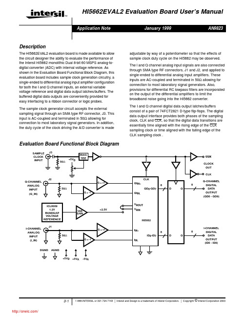
The HI5662 evaluation board is a four layer board with a layout optimized for the best performance of the ADC. Included in the application note are electrical schematics of the evaluation board, a component parts list, a component placement layout drawing and reproductions of the various board layers used in the board stack-up. The user should feel free to copy the layout in their application. Refer to the component layout and the evaluation board electrical schematic for the following discussions.
HI5662EVAL2 Evaluation Board User’s Manual
TM
Application Note
January 1999
AN9823
Description
The HI5662EVAL2 evaluation board is made available to allow the circuit designer the ability to evaluate the performance of the Intersil HI5662 monolithic Dual 8-bit 60 MSPS analog-todigital converter (ADC) with internal voltage reference. As shown in the Evaluation Board Functional Block Diagram, this evaluation board includes sample clock generation circuitry, a single-ended to differential analog input amplifier configuration for both the I and Q channel inputs, an external variable voltage reference and digital data output latches/buffers. The buffered digital data outputs are conveniently provided for easy interfacing to a ribbon connector or logic probes.
27938;中文规格书,Datasheet资料
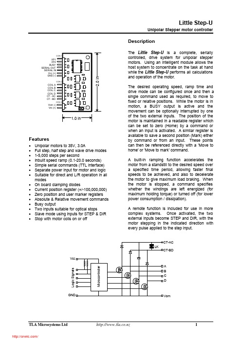
Little Step-UUnipolar Stepper motor controllerTLA Microsystems Ltd 1Features• Unipolar motors to 35V, 3.0A• Full step, half step and wave drive modes • 1-5,000 steps per second• Inbuilt speed ramp (0.1-20.0 seconds)• Simple serial commands (TTL interface)• Separate power input for motor and logic • Suitable for direct and L/R operation in all modes• On board clamping diodes• Current position register (+/-100,000,000)• Zero position and user marker registers • Absolute & Relative movement commands • Busy output• Two inputs suitable for optical stops• Slave mode using inputs for STEP & DIR •Stop with motor coils on or offDescriptionThe Little Step-U is a complete, serially controlled, drive system for unipolar stepper motors. Using an intelligent module allows the host system to concentrate on the task at hand while the Little Step-U performs all calculations and operation of the motor.The desired operating speed, ramp time and drive mode can be configured once and then a single command used as required, to move to fixed or relative positions. While the motor is in motion, a BUSY output is active and the movement can be optionally interrupted by one of the two external inputs. The position of the motor is maintained in a readable register which can be set to zero (Home) by a command or when an input is activated. A similar register is available to save a second position (Mark) either by command or from an input. These points can then be referenced directly with a 'Move to home' or 'Move to mark' command.A built-in ramping function accelerates the motor from a standstill to the desired speed over a specified time period, allowing faster final speeds to be achieved, and also to decelerate the motor to give maximum load braking. When the motor is stopped, a command specifies whether the windings are left energized (for maximum holding torque) or turned off (for lower power consumption / dissipation).A remote function is included for use in more complex systems. Once activated, the two external inputs become STEP and DIR, with the motor stepping in the indicated direction withevery pulse applied to the step input./IP1/IP2BUSYSERIAL OUT SERIAL INVcc (+)GND (-)COIL A COIL B COIL C COIL D CT - AC CT - BDVm (+)A B C D VomL o g i c S i g n a l s/DC CharacteristicsCharacteristic Symbol Min Typ Max Unit NotesLogic Supply Voltage V CC 4.5 5.0 5.5VVcc risetime t VCC0.05V/ms1Logic supply current I CC 1.5 3.0mAInput Low Voltage V IL0.0 1.0VInput High Voltage V IH 4.3Vcc VOutput Low Voltage V OL0.6VOutput High Voltage V OH 4.3VIP1/2 Source Current I OL 1.0mAMotor Voltage V M50VMotor current I M 3.0AMotor resistance R M 2.8ΩClamp diode current I CL250mAStep rate F STEP15000steps/secSpeed Error F ERR+/- 0.5%2Comms bit rate F BIT2400bpsBUSY rise/fall time T RF1025nsResponse time to IP1/2T INP1ms3DIR hold time T DIR8usMax Slave step rate F EXT10000steps/sec4Operating temp t OP070°C5Storage temp t ST-40100°C[1]Required to ensure reliable startup.[2]As a percentage of requested speed[3]Response to IP is lesser of 1ms or 1 step[4]If no comms while stepping. Max = 6000 steps/sec with comms[5]Refer loading derating graphPin functionsConnector 1Pin Function/IP1Optional input 1. Set home. Emergency stop./IP2Optional input 2. Set mark. Emergency stop.BUSY Output - High when motor movingSERIAL OUT Data from Little step-U to controller. TTLSERIAL IN Data from controller to Little Step-U. TTLVcc Supply to logic circuitsGND Supply ground. Common with motor circuits.Connector 2Pin FunctionA Winding A outputB Winding B outputC Winding C outputD Winding D outputCT-AC Common for windings A & CCT-BD Common for windings B & DConnector 3Pin FunctionV OM Motor supply ground. Common with logic circuitsV M Motor Supply +2Little Step-U /Hardware ConnectionPower SupplyThe Little Step-U divides the circuitry into two distinct sections with separate power suppliesrequired for the motor drive and the logic. The logic/control section must be powered by aregulated 5V supply applied to the VCC and GND pins. The motor power supply voltage isdictated by the motor characteristics and is connected to the VM(+) and VOM(-) pins. TheGND and VOM pins are connected on the circuit board as a common reference. The motorpower supply must have sufficient capacity for the motor and if the power supply is notphysically close to the motor/controller, a capacitor (eg. 4700uF) may be required at thecontroller to ensure smooth operation of the motor.Motor ConnectionThe motor connector has 4 connections (A, B, C & D) that are switched to ground in thesequence required to cause the motor to step. Note that stepper motor manufacturers haveseveral methods of labelling the connections to the motor. The Little Step-U labels the pins inthe sequence they are switched when operating the motor with one coil on at a time and drivingin a clockwise direction. ie. A, then B, then C, then D and back to A. The centre taps of thetwo coils are connected to CT-AC and CT-BD, corresponding to the common connection of coilsA & C and coilsB & D respectively. These two connections provide the freewheel diodes foreach of the motor coils and are connected on the circuit board.IMPORTANT: A poor or intermittent connection to any of the stepper motor terminals can resultin destructive voltages being generated and causing permanent damage to the Little Step-U.Similarly, do not connect or disconnect any stepper motor connections while power is applied.The connection point between CT-AC and CT-BD is indicated on the circuit board by thedesignator "LK". This track can be cut and rejoined by soldering a wire between two pads ifneeded. In most cases this isn't required but is provided for applications using and L/xRconfiguration in half step mode.Interface connectionsThe Little Step-U acts on commands received serially from a host controller via the SERIAL INpin. This is an asynchronous interface operating at 2400 bits per second, 8 data bits (LSBfirst), 1 stop bit and no parity. The signal levels are TTL. Some commands illicit a responseand these are sent via the SERIAL OUT pin using the same protocol and signal levels as theSERIAL IN pin.When a command has been sent to the Little Step-U that causes the motor to move, the BUSYpin will be high while the motor is in motion.Two input pins are provided for use with stepper operation in the form of limit or home switchesor can be used as general inputs which can be read by software. These pins accept logic levelinputs and will source 1mA when pulled low, making them suitable for direct connection to theoutput of opto-couplers.TLA Microsystems Ltd 3 /Software commandsCommunication with the Little Step-U is by a TTL level serial interface at 2400bps. Allcommands must begin with a "{" character and end with a "}" Characters outside of the braces(including carriage return and line feeds) are ignored. Responses are enclosed by "[" and "]"characters.A - SET SPEEDSyntax{Axxxxx}Default value100 steps/secSets the maximum speed in steps per second for any commands that follow. Thenumeric value can be any number from 1 to 5000.B - SET RAMP TIMESyntax{Bxxx}Default value0 secondsThe Little Step-U has a built in function to accelerate and decelerate the stepper motorto/from the speed specified by the command above. This command sets the amount oftime in tenths of a second that the motor will accelerate to that speed. Valid numbersare 0 to 200 being 0.0 to 20.0 seconds in 0.1 second increments.Any move function that utilises the ramping facility will accelerate and decelerate at therate defined by this command. The distance moved includes the steps used to ramp upand ramp down so a move of 1000 steps will move exactly that amount. If the number ofsteps requested is less than the number required to ramp to full speed and ramp downagain, the Little Step-U will accelerate at the same rate until it is half way to itsdestination and then ramp down again to stop at the commanded position.See the discussion on ramping after the command descriptions.C - SET STEP MODESyntax{Cx}Default value0 (Full step drive)Stepper motors can be driven by powering the windings sequentially using three differenttechniques. The method used is specified by this command with x being 0, 1 or 2.{C0}Full stepFor every step, two windings are energised.Step Coil A Coil B Coil C Coil D1ON ON Off Off2Off ON ON Off3Off Off ON ON4ON Off Off ON{C1}WaveEach step has only one winding energised.Step Coil A Coil B Coil C Coil D1ON Off Off Off2Off ON Off Off3Off Off ON Off4Off Off Off ON4Little Step-U /{C2}Half stepEach alternate step has one or two windings energised giving the motor twicethe number of steps per revolution.Step Coil A Coil B Coil C Coil D1ON Off Off Off2ON ON Off Off3Off ON Off Off4Off ON ON Off5Off Off ON Off6Off Off ON ON7Off Off Off ON8ON Off Off ONWhen the mode is changed to or from Half step, the position, mark and speed values areadjusted accordingly so that the motor will turn at the same rotational speed and themechanical positions remain unchanged.Example: A 200 step/rev motor is being used. The current position is 3600, speed is setat 200 steps per second and there is a mark at 1200. When the mode is changed fromfull-step to half step, the speed value will be 400 (giving the same number of revolutions ofthe motor per second). The current position register and the mark register will containthe values 7200 and 2400 respectively.D - GO TO ABSOLUTE POSITIONSyntax{Dxxxxxxxx}At anytime after powerup, the Little Step-U keeps track of its current position in steps.This command instructs the Little Step-U to calculate the direction and number of stepsrequired to move to another position and then it performs the move. At the end of themove, the position will be the number specified in this command. The value can be anynumber from -10000000 to +10000000, including 0. The number may be preceded by a"+" or "-" as required, but must not include a comma or decimal point.Example: If the current position is 2500, a command of {D-1000} will cause the motor torun counter-clockwise for 1500 steps, stopping at position 1000.E - GO TO RELATIVE POSITIONSyntax{Exxxxxx}This command is similar to the "D" command in respect to the numeric parameter, butcommands the motor to move to a position relative to its current position. Positivenumbers are clockwise and negative numbers are counter-clockwise.Example: If the current position is 2500, a command of {E1000} will cause the motor torun 1000 steps clockwise to end at position 3500.F - GO TO ABSOLUTE POSITION WITH INPUTS 1 & 2 AS STOPSSyntax{Fxxxxxx}This command is the same as the "D" command except that the two input pins aremonitored. If either of them is pulled low during the move, the motor will be deceleratedto a stop at the rate defined in the RAMP command (B). The position register will reflectthe current position when the motor has stopped. These inputs are level sensitive so if a“F” command is used when one of the inputs is low, the motor will stop immediately.Note: Allowing the motor to continue to running past a stop indicator is done for tworeasons; This method allows the motor to provide maximum braking torque duringdeceleration and the position register integrity is maintained.TLA Microsystems Ltd 5 /Example: If the current position is 2500 and a limit switch attached to I/P2 is at position5000, the command {F8000} will result in the motor stopping at position 5087 (dependingon the SPEED and RAMP settings).G - GO TO RELATIVE POSITION WITH INPUTS 1 & 2 AS STOPSSyntax{Gxxxxxx}This command is the same as the "E" command except that the two input pins aremonitored as in the command above.Example: If the current position is 2500 and a limit switch attached to I/P1 is at the homeposition (0), the command {G-5000} will result in the motor stopping at position -87(depending on the SPEED and RAMP settings).H - GO CLOCKWISE UNTIL INPUT 2Syntax{H}This command is used to find a limit stop connected to I/P2 and has no numericparameter. The motor will accelerate at the rate determined by the RAMP setting, up tothe SPEED setting and not stop (ramp down) until I/P2 is pulled low.Example: The motor is at position 28 and a limit switch is at position 1000. The SPEEDhas been set to a slow value and RAMP set to 0. After an {H} command the position is1000.J - GO COUNTER-CLOCKWISE UNTIL INPUT 1 AND ZERO POSITIONSyntax{J}The J command is similar to the H command above except that the direction is reversedand I/P1 is used to halt the movement. When the movement is stopped, the positionregister is cleared to 0 to mark this position as "Home".Example: The motor is at an unknown position and a {J} command is used at a slowspeed and 0 RAMP rate. At the end of the movement (dictated by I/P1) the positionregister is 0.K - GO CLOCKWISE UNTIL INPUT 2 AND MARK POSITIONSyntax{K}The motor runs continuously in a clockwise direction until stopped by I/P2 being pulledlow. When this occurs, the position is recorded in the MARK register.Example: The motor has been moved to the home position using the {J} command.Issuing a {K} command will run the motor and when it has stopped, the position of theother limit switch has been recorded.M - GO TO THE MARK POSITIONSyntax{M}This command instructs the Little Step-U to move to the absolute position held in the"Mark" register. The contents of this register is set to 0 when the device is powered onand can be set using the "K" or "R" commands. As with the "D" (Go to absoluteposition) command, the controller will determine the direction and will use the Ramp andSpeed settings to move to that position.Example: The Little Step-U is being used in a component placement machine and theposition to pick up the next component is known to always be 123456. After eachplacement, a {M} command will place the pickup head over the next component to beplaced.6Little Step-U /N - GO TO THE HOME POSITIONSyntax{N}Sending an "N" command will cause the Little Step-U to move the motor to the 0, orhome position. The position register defaults to 0 when the device is powered on and canbe set to 0 by the "J" or "Q" commands.Example: A Little Step-U is being used to position a print head in a dot matrix printer. Ateach Carriage Return in the data being printed, an {N} command is issued to return thehead to the left margin, ready for the next line.P - SET OFF STATE POWERSyntax{Px}When the motor is not being moved, the coils can be left energised for maximum holdingtorque or turned off to reduce power consumption and motor heating. This command setsthe state as off {P0} or on {P1} and will remain that way until changed with another "P"command. Power on default is off.Example: A motor is being used in a high vibration environment and retaining position ismore important than power consumption. The {P1} command ensures maximum holdingtorque.Q - SET HOME POSITIONSyntax{Q}This command unconditionally sets the position register to 0. All position information andabsolute moves become relative to this new home position.Example: A drilling sequence needs to be repeated several times over a panel. The totalsize of the program can be reduced by moving the offset amount, resetting the homeposition with the {Q} command and repeating the same sequence.R - SET MARKSyntax{R}This command instructs the Little Step-U to remember the current position. It is used inconjunction with the {M} command which will return the motor to this same positionregardless of any intervening moves.Example: A stepper motor is being used in a piece of hastily constructed test equipmentto rub an abrasive over a surface. The distance is found by trial and error and a mark isset with the {R} command. The experiment can then be run using the {Q} (Go to home)and {R} (Go to mark) commands in a loop.S - SWITCH TO REMOTE MODESyntax{S}The Little Step-U can be operated as simple translator/drive for use in systems withenhanced motion control capability or for the purposes of experimentation. This mode ofoperation is entered by sending the {S} command. Input pin 1 will then act as the STEPinput and Input pin 2 will act as a DIRection input.On each high to low transition (falling edge) of the STEP input, the motor will move onestep in the direction indicated by the DIR input. A high on the DIR input will cause themotor to step clockwise and a low, counter-clockwise. This input must be stable whenSTEP is taken low and for tDIR afterwards. When in REMOTE mode, the mode settingsthat were set with the {C} command (wave, full, half step) remain in force and the position TLA Microsystems Ltd 7 /register is updated with each step. The {S} command will turn the motor windings on,regardless of the value set by the {P} command.Example: During the commissioning phase of a machine, the operator wishes to move toa target position one step at a time using a pushbutton. The {S} command is sent andthe microcontroller is used to debounce each button press and apply a single pulse.When the desired destination is reached, the position is read using the {U} command.T - RETURN FROM REMOTE MODESyntax{T}When the Little Step-U is operating in the REMOTE mode, sending a {T} will return to thestandard operating mode. The position register contents are valid and the motor windingswill be powered on or off according to the value previously set by the {P} command.Example: Once the setup phase described above has been completed, a {T} commandreadies the controller for full speed operation.U - SHOW CURRENT STATUSSyntax{U}Returns[aaaa,bbbb,ccc]The {U} command instructs the Little Step-U to send the current values of the Position,Speed and Ramp registers back to the controller. The data consists of enclosing squarebrackets ("[" and "]") containing the three (decimal) values separated by commas.Example: A stepper is being used to move a print head mechanism. In order todetermine the paper width the user has selected, the motor is moved to one stop andzeroed and then moved slowly to the other stop with RAMP set to 0. When the motorstops (BUSY goes low), the position is retrieved with the {U} command. The controllercan then use this value to scale the print head movement commands and ensure that animage will fit on the page.V - SHOW STATE OF INPUT PINSSyntax{V}Returns[a,b]The {V} command returns the current state of the two input pins in the form of "0" for alow input and "1" for a high.Example: An {G-1000} command is issued which instructs the Little Step-U to move1000 steps counter-clockwise from the current position and to stop if it encounters a lowinput on either IP1 or IP2. Checking that the complete move was made successfully ismade easier by only having to check two single digits with the {V} command, thansubtracting the current position from the earlier position and checking the result.Multi-parameter commandsMovement related commands have the option of including speed, ramp time and/or step modevalues in the form of {X,speed,ramp,mode} where X is the command listed below and speed,ramp and mode are valid values as described for the A, B and C commands above. Eachparameter is separated by a comma and may either be a value or no value (without spaces) ifthat parameter is to remain unchanged. Any setting changed by using a command in this formwill remain at the new value for any subsequent commands unless explicitly changed.D GO TO ABSOLUTE POSITIONE GO TO RELATIVE POSITION8Little Step-U /TLA Microsystems Ltd 9F GO TO ABSOLUTE POSITION WITH INPUTS 1 & 2 AS STOPSG GO TO RELATIVE POSITION WITH INPUTS 1 & 2 AS STOPS H GO CLOCKWISE UNTIL INPUT 2J GO COUNTER-CLOCKWISE UNTIL INPUT 1 AND ZERO POSITION K GO CLOCKWISE UNTIL INPUT 2 AND MARK POSITION M GO TO THE MARK POSITION N GO TO THE HOME POSITIONExamples:{D-2000,200,5}Go to absolute position -2000 with a maximum speed of 200 steps per second, accelerating to that speed over a period of 0.5 seconds and use the currently set drive mode.{N,,,0}Go to the HOME position using the current speed and ramp settings but change the drive mode to full step.Ramping or Trapezoidal speed profile.The ability to accelerate a stepper motor over a period of time, greatly improves the useful range of operations the motor can perform. Not only does this allow the motor to reach higher speeds,but also reduces wear on mechanical components. While acceleration is defined as a change in speed over a period of time (steps/sec/sec), it is easier to think of the motor accelerating to a desired speed over a defined time period, so the B command is used in this manner.The graph below illustrates a typical move where the final speed, ramp time and destination position have been specified. Both the position (in steps) and the speed (in steps per second)show how the motor moves slowly at the beginning, at the maximum rate for the majority of the move and then transitions smoothly into the deceleration phase, before coming to a stop at the desired position. Because of the shape of the curve, the speed plot is known as a trapezoidal speed profile.When the distance to be moved is less than that required to ramp up to full speed and then ramp down again, the acceleration rate is kept the same and half way through the move, the Little Step-U will begin the deceleration. An example is illustrated below. The speed and ramp values are unchanged for two discrete move operations. The first is long (far) enough for the motor to reach the specified operating speed but because Move 2 is shorter, the motor transitions directly from accelerating in speed to the deceleration profile.Final Speed/PositionMove 1Move 2TimeThe ramp function used in the Little Step-U is a piecewise, linear ramp of frequency in 64 steps.The motor is run at each of these speeds for a period that is 1/64 of the ramp time requestedwith the {B} command.If long ramp periods are used with a high final speed, the steps are discernible to the ear but stillachieve the desired effect of not accelerating the motor at excessive rates.When using relatively slow final speed settings with short ramp times, the situation arises wherethe first few steps take longer than the allocated time.For example, a motor accelerating to a final speed of 640 steps/sec will run at 10 steps/sec, 20,30, etc. At 10 steps/sec, each step takes 100ms. If the ramp time setting is 2 (for 200ms),clearly a problem has arisen as the first step has used half of the ramp time for one step.The Little Step-U addresses this situation by dividing the ramp time into 64ths. If the length ofone step at the required speed is less than 1/64 of the ramptime, that step rate is skipped.In the example above, 1/64 of the total ramp time (200ms) is 3.1ms which is the period of onestep at 320 steps/sec, so the first step will be at the 320 steps/sec rate, the next at 330steps/sec, etc. This means that the motor doesn’t actually turn until halfway through theramping period (320 = half of the final speed 640). Rather than have the motor doing nothing forthe duration of this dead period, the delay is bypassed and the motor will appear to startimmediately at 320 steps/sec and take only 100ms to get to the final speed, even though the Bcommand specified 200ms.The net result is that the motor acceleration in steps per second per second is still the sameand this is the important parameter. Having it specified as a time to reach final speed is aneasier concept to grasp and is also a simple figure to calculate from a required accelerationrate.Ramping and forced stopsWhen the motor is forced to a stop from an external input (IP1 or IP2) and a ramp value otherthan zero has been specified, the motor will begin decelerating at that point. Obviously the finalresting position will be different from that when the input occurred. Where the input is used tospecify a position, the register is updated when the input occurs, not when the motor completesthe ramp down.For example, the {J} command runs the motor counter-clockwise until IP1 is pulled low andmarks that position as zero. If the ramp value is 0, the motor will stop there and the positionregister will hold 0. If a ramp period has been specified, the position register will hold a negativevalue, indicating the number of steps used to decelerate to a stop. The {N} command (Go to theHome position) can then be used to move the motor to where the input occurred.10Little Step-U /分销商库存信息: PARALLAX 27938。
2N3906-AP;中文规格书,Datasheet资料

2N3906PNP General Purpose AmplifierFeaturesElectrical Characteristics @ 25°C Unless Otherwise SpecifiedSymbolParameterMin MaxUnits OFF CHARACTERISTICSV (BR)CEO Collector-Emitter Breakdown Voltage* (I C =1.0mAdc, I B =0)40 Vdc V (BR)CBO Collector-Base Breakdown Voltage (I C =10µAdc, I E =0)40 Vdc V (BR)EBO Emitter-Base Breakdown Voltage (I E =10µAdc, I C =0) 5.0VdcI BL Base Cutoff Current(V CE =30Vdc, V BE =3.0Vdc)50 nAdc I CEXCollector Cutoff Current (V CE =30Vdc, V BE =3.0Vdc)50 nAdcON CHARACTERISTICSh FEDC Current Gain*(I C =0.1mAdc, V CE =1.0Vdc) (I C =1.0mAdc, V CE =1.0Vdc) (I C =10mAdc, V CE =1.0Vdc) (I C =50mAdc, V CE =1.0Vdc) (I C =100mAdc, V CE =1.0Vdc)60801006030300V CE(sat)Collector-Emitter Saturation Voltage (I C =10mAdc, I B =1.0mAdc) (I C =50mAdc, I B =5.0mAdc)0.250.4VdcV BE(sat)Base-Emitter Saturation Voltage (I C =10mAdc, I B =1.0mAdc) (I C =50mAdc, I B =5.0mAdc)0.650.850.95VdcSMALL-SIGNAL CHARACTERISTICSf T Current Gain-Bandwidth Product(I C =10mAdc, V CE =20Vdc, f=100MHz) 250 MHz C obo Output Capacitance(V CB =5.0Vdec, I E =0, f=100k Hz) 4.5 pF C ibo Input Capacitance(V BE =0.5Vdc, I C =0, f=100kHz)10.0pF NFNoise Figure(I C =100µAdc, V CE =5.0Vdc, R S =1.0k Ωf=10Hz to 15.7kHz)4.0dB SWITCHING CHARACTERISTICSt dDelay Time (V CC =3.0Vdc, V BE =0.5Vdc 35ns t r Rise Time I C =10mAdc, I B1=1.0mAdc)35 ns t s Storage Time (V CC =3.0Vdc, I C =10mAdc 225 ns t fFall Time I B1=I B2=1.0mAdc)75ns*Pulse Width≤ 300µs, Duty Cycle ≤ 2.0%omp onents 20736Marilla Street Chatsworth! "# $ % ! "#Revision: D 2012/07/13TMMicro Commercial Componentswww.mccsemi .com1 of 5x Marking:Type numberx Capable of 600mW of Power Disspation and 200mA Ic x Through Hole Package x Moisure Sensitivity Level 1x Epoxy meets UL 94 V-0 flammability rating • Lead Free Finish/RoHS Compliant ("P" Suffix designates RoHS Compliant. See ordering information)2N3906DC Current Gain vs Collector Current h FEI C (mA)40801201602002200.1110100Base-Emitter ON Voltage vs Collector Current V BE(ON) - (V)I C - (mA)00.20.40.60.81.01.20.11.010100Collector-Emitter Saturation Volatge vs Collector Current Base-Emitter Saturation Voltage vs Collector CurrentV CE(SAT) - (V)V BE(SAT) - (V)00.10.20.30.40.50.61.01010010000.20.40.60.81.01.21.41.0101001000I C - (mA)I C - (mA)Collector-Base Diode Reverse Current vs Temperature Common Base Open Circuit Input andOutput Capacitance vs Reverse Bias Voltage I CBO - (mA)T J - (°C)Volts - (V)pF0.11.010100255075100125150V CB = 20V 024681.00.11.010C OBO C IBOT A = 25°CTO-92I C /I B = 10T A = 25°CI C /I B = 10T A = 25°CV CE = 1.0VV CE = 5.0VT A = 25°CT A = 100°C Revision: D 2012/07/13TMMicro Commercial Componentswww.mccsemi .com2 of 52N3906f - (kHz)Maximum Power Dissipation vs Ambient Temperature Noise Figure vs Source ResistanceP D(MAX) - (mW)T A - (°C)TO-92SOT-230200400600800050100150200NF - (dB)R S - (k Ω)0246810120.11.010100I C = 1.0mAI C = 100µAV CE = 5.0V f = 1.0kHzContours of Constant Gain Bandwidth Product (f T )Current GainV CE - (V)I C - (mA)h feI C - (mA)V CE = 10V f = 1.0kHz048121620240.11.0101001010010000.11.010Noise Figure vs Frequency Switching Times vs Collector Current NF - (dB)T - (ns)I C - (mA)1.01010010001.010100I B1 = I B2 = I C /10t st ft r t dV CE = 5.0VI C = 100µA R S = 200ΩI C = 1.0mA R S = 200ΩI C = 100µA R S = 2.0k Ω0.11.010100123456*100MHz increments from 100 to 700, 750 and 800MHzRevision: D 2012/07/13TMMicro Commercial Componentswww.mccsemi .com3 of 52N3906Input Impedance Output Admittanceh ie - (k Ω)I C - (mA)I C - (mA)h oe - (µΩ)V CE = 10V f = 1.0kHzV CE = 10V f = 1.0kHz0.11.0100.11.0100.11.010101001000Voltage Feedback Ratio Turn On and Turn Off Times vs Collector Currenth fe - (X10-4)I C - (mA)I C - (mA)T - (ns)1.0101000.1 1.0101.01010010001.010100t on I B1 = I C /10V BE(OFF) = 0.5V t off I B1 = I B2 = I C /10t offt onRevision: D 2012/07/13TMMicro Commercial Componentswww.mccsemi .com4 of 5Revision: D 2012/07/13Micro Commercial Componentswww.mccsemi .com5 of 5Part Number-BP Bulk: 100Kpcs/CartonOrdering Information :***IMPORTANT NOTICE***Micro Commercial Components Corp. reserve s the right to make changes without further notice to any product herein to make corrections, modifications , enhancements , improvements , or other changes . Micro Commercial Components Corp . does not assume any liability arising out of the application or use of any product described herein; neither does it convey any license under its patent rights ,nor the rights of others . The user of products in such applications shall assume all risks of such use and will agree to hold Micro Commercial Components Corp . and all the companies whose products are represented on our website, harmless against all damages.***LIFE SUPPORT***MCC's products are not authorized for use as critical components in life support devices or systems without the express writtenapproval of Micro Commercial Components Corporation.***CUSTOMER AWARENESS***Counterfeiting of semiconductor parts is a growing problem in the industry. Micro Commercial Components (MCC) is taking strong measures to protect ourselves and our customers from the proliferation of counterfeit parts. MCC strongly encourages customers to purchase MCC parts either directly from MCC or from Authorized MCC Distributors who are listed by country on our web page cited below . Products customers buy either from MCC directly or from Authorized MCC Distributors are genuine parts, have full traceability, meet MCC's quality standards for handling and storage. MCC will not provide any warranty coverage or other assistance for parts bought from Unauthorized Sources. MCC is committed to combat this global problem and encourage our customers to do their part in stopping this practice by buying direct or from authorized distributors.DevicePackingPart Number-AP Ammo Packing: 20Kpcs/Carton 3分销商库存信息: MICRO-COMMERICAL-CO 2N3906-AP。
19665;中文规格书,Datasheet资料

Dual-Wire Dual-Operator Programmable Monitor DescriptionThe patented* Desco Dual-Wire Dual-OperatorProgrammable Monitor monitors two operators and two ESD work worksurfaces eliminating the need for periodic Figure 1. Desco 19665 Dual-Wire Dual-Operator Programmable MonitorFeatures and ComponentsTECHNICAL BULLETIN TB-3019Made in theUnited States of AmericaFigure 2. Dual-Wire Dual-Operator Programmable CBDE FG H I J K LFRONT VIEWBACK VIEWOperation1. Monitoring of the operators will remain in the STANDBY condition until a wrist cord is plugged into the operator remote. STANDBY mode is indicated by a blinking yellow operator LED.10mm snap needs to pierce and clinch bottom side of mat. Snap needs to be at least 12" apart or 72" max. 10mm snap needs to pierce and clinch bottom side of mat. Snap needs to be at least 12" apart or 72" max.OPERATOR 1WORKSURFACEOPERATOR 2WORKSURFACE10mm PUSH & CLINCH SNAP10mm PUSH & CLINCH SNAPBENCH GROUNDMAT 1 WIRING WHITE CABLEMAT 2 WIRING BLACK CABLEWRIST STRAP MONITORWRIST STRAP MONITORELECTRIC GROUNDOPERATOR 2REMOTE JACK BLACK CABLEOPERATOR 2REMOTE JACK WHITE CABLE Screw allows ground cord to be bolted to mat; keeps cord from disconnecting.Figure 3. Installing the Dual-Wire Dual-Operator Programmable MonitorororFigure 4. Connecting a dual-wire wrist strap to the operator remoteSETTING THE OPERATOR TEST VOLTAGE AND TEST LIMITThe Dual-Wire Dual-Operator Monitor’s operator test voltage and high test limit can be set to different values. The operator test voltage can be set to either +5V or +8V, and the operator high test limit can be set to either 10 megohms or 35 megohms. The default voltage is +8V, and the default operator high test limit is 10 megohms. These settings are controlled by a set of 3 switches located inside the monitor’s enclosure.NOTE: Desco recommends re-calibration of the monitor should either setting be changed. See the “Calibration” section for more information.To gain access to these switches, remove the monitor’s cover and position the monitor so the PCB matches the orientation shown in Figure 5. Switches SW1 and SW2 control the operator test voltage. Switch SW3 controls the operator high test limit.Operator Test Voltage+5VSW1 Position: RIGHTSW2 Position: LEFT+8VSW1 Position: LEFTSW2 Position: RIGHTOperator High Test Limit10 megohmsSW3 Position: RIGHT35 megohmsSW3 Position: LEFTCalibrationFrequency of recalibration should be based on the critical nature of those ESD sensitive items handled and the risk of failure for the ESD protective equipment and materials. In general, Desco recommends that calibration be performed annually.Use the EMIT 50524 Limit Comparator for Dual-Wire Monitors to perform periodic testing (once every 6-12 months) of the Dual-Wire Dual-Operator Programmable Monitor. The Limit Comparator can be used on the shop floor within a few minutes virtually eliminating downtime, verifying that the monitor is operating within tolerances. See TB-6542 for more information.Figure 5. Switches SW1, SW2 and SW3 inside the monitor’s enclosure Figure 6. EMIT 50524 Limit Comparator for Dual-Wire MonitorsNIST CalibrationDesco provides a basic, National Institute of Standardsand Technology (NIST) traceable calibration for theproducts that we manufacture. This is sometimesreferred to as a Level 1 calibration.For more on National Institute of Standards andTechnology see:/index.htmlFor more information on the calibration that Desco’sprovides for products that we manufacture see:/Calibration.aspxSpecificationsOperating Voltage 12 VDCOperating Temperature 32°F - 104°F (0 - 40°C)Monitor Dimensions 4.4" x 4.7" x 2.1"(11.2cm x 11.9cm x 5.3cm)Monitor Weight 1.1 lbs (0.5 kg)TEST VOLTAGESOperator +8 V** or +5 VWorksurface 200 mVTEST LIMITSOperator Low Fail: < 1.72 megohmsPass: 2 - 9 megohms**High Fail: > 11.5 megohms**orPass: 2 - 30 megohmsHigh Fail: > 40 megohmsWorksurface Pass: < 3.5 megohmsFail: > 3.8 megohms**DefaultFigure 7. Operator Remote dimensionsReplacement remotes are available as EMIT itemnumbers 50525 and 50526.分销商库存信息: DESCO19665。
AQZ205;AQZ107;AQZ202;AQZ204;AQZ207;中文规格书,Datasheet资料
TYPICAL APPLICATIONS
• Traffic signals • Measuring instruments • Industrial machines
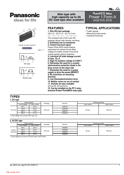
Height includes standoff
CAD Data
mm inch
1-Βιβλιοθήκη +23
DC type
-
+
4
1
-
AC/DC type
+
Item LED operate current Input LED turn off current LED dropout voltage On resistance Output Off state leakage current Maximum Maximum Typical Maximum Turn on time* Typical Maximum Transfer characteristics Typical Turn off time* Maximum I/O capacitance Initial I/O isolation resistance Maximum operating speed Vibration resistance Shock resistance Typical Maximum Minimum Maximum Minimum Minimum Ciso Riso — — — Toff 3.0 ms 0.8 pF 1.5 pF 1,000 M 0.5 cps 10 to 55 Hz at double amplitude of 3 mm 4,900 m/s2 {500 G}1 ms 0.22 ms Ton 5.64 ms 5.65 ms 2.57 ms 3.88 ms 10.0 ms 0.21 ms 0.10 ms 0.08 ms ILeak 2.46 ms Typical Maximum Minimum Typical Typical Maximum Typical Ron Symbol IFon IFoff VF 0.11 0.18 AQZ202 AQZ205 AQZ207 1.0 mA 3.0 mA 0.4 mA 0.9 mA 1.25 V (1.16 V at IF = 10 mA) 1.5 V 0.23 0.34 10 A 2.40 ms 1.12 ms 1.65 ms 0.7 1.1 2.1 3.2 AQZ204 IL= 100 mA VL= 10 V IL= 100 mA VL= 10 V IF = 50 mA IF = 10 mA IL =Max. Within 1 s on time IF = 0 mA VL = Max. IF = 10 mA IL = 100 mA VL = 10 V IF = 5 mA IL = 100 mA VL = 10 V IF = 5 mA or 10 mA IL = 100 mA VL = 10 V f = 1 MHz VB = 0 V 500 V DC IF = 10 mA Duty factor = 50% IL = Max., VL = Max. 2 hours for 3 axes 3 times for 3 axes Condition