3316, 规格书,Datasheet 资料
MC34167MC33167中文资料
MC34167 MC331671简介该MC34167, MC33167系列单片电源开关可用于dc–to–dc优化调节器申请.这些器件的固定频率,电压模式稳压器包含了所有的积极作用需要直接和实施step–down以最小的转换数量voltage–inverting外部元件.它们也可以用于成本效益在step–up转换器应用.潜在市场包括汽车,计算机,工业和成本敏感的消费产品.每一个设备的部分介绍给下面与代表框图所示图13.2振荡器振荡器频率内部编程72 kHz的电容CT和修剪电流源.该充放电率控制在产生一个95%在开关输出的最大占空比.在CT的放电,振荡器产生内部消隐脉冲持有的反相输入与门高,禁用输出开关晶体管.标称振荡器峰值和山谷门槛4.1 V和2.3 V分别.3脉宽调制器脉宽调制器由一个比较器振荡器斜坡电压施加到非反相输入端,而误差放大器的输出应用到反相输入.输出开关导通时启动CT检查排放到振荡器峰谷电压.至于收费的CT电压超过误差放大器的输出,锁存复位,终止输出晶体管的导通时间振荡器的ramp–up时期.这PWM /锁存结合防止在给定的多输出脉冲振荡器时钟周期.数字6和14说明开关输出电压与占空比的补偿.4电流检测该系列采用MC34167当前cycle–by–cycle限制,作为保护手段输出开关晶体管从过度紧张.在每个周期视为一个单独的情况.电流限制是通过监测输出开关晶体管的电流传导期间建设,并经检测过流情况,请立即关闭为振荡器的ramp–up期内开关.集电极电流转换为电压由内部微调电阻和对一个参考比较由电流检测比较器.当电流限制达到阈值,比较器重置PWM 锁存.限流门限点往往设在6.5 A.图9说明开关与输出电流限制门槛温度.5误差放大器和参考一个误差放大器的高增益提供了访问反相输入和输出.该放大器具有典型dc电压增益80 dB,和单位增益带宽600 kHz与相边缘 70度(图3).同相输入偏置内部5.05 V参考并且不固定了.参考具有精度±2.0%在室温下.以提供负载5.0 V中,参考编程50以上mV 5.0 V补偿在电缆的电压降和1.0%从连接器转换器输出.如果转换器设计需要一个输出电压高于5.05 V,电阻更大R1必须加入形成一个分压网络的反馈输入中所示数字13和18.了确定输出方程与分压网络的电压为:Vout+5.05R2R1)1外部回路补偿所需的转换器稳定.一个简单的low–pass滤波器是由连接电阻(R2)从稳压输出到反相输入,以及一系列resistor–capacitor (RF, CF)之间Pins 1和5.补偿网络的元件值显示在电路的申请被选定为each在稳定工作条件下进行测试.该step–down转换器(图18)是最容易补偿稳定.该step–up(图20)和voltage–inverting(图22)配置运作,连续导反激式转换器,而且更难以弥补.该最简单的方法来优化网络是补偿观察输出电压的负载响应一步变化,而调整临界阻尼RF和CF.该最终电路应验证以下四个稳定边界条件.这些条件是最小和最大输入电压,最小和最大负载.通过箝位的电压误差放大器的输出(引脚5)不到150 mV,内部电路将放置到一个低功耗待机模式,从而将权力电源电流36µA与12 V电源电压.图10说明了备用电源电流与电源电压.误差放大器的输出有一个100µA电流源pull–up,可用于实现soft–start.图17显示充电电流源通过一个电容CSS系列二极管.该二极管断开从反馈CSS回路电阻时1.0 M操作它上面的收费销5.范围开关输出输出开关晶体管的设计最大的40 V,以最小的峰值集电极电流时5.5 A.配置为step–down或voltage–inverting应用,如在图18和22,电感会把偏置的输出整流开关关闭时.整流器与较高的正向电压降或长期拖延的时间应该打开不能使用.如果发射器被允许去充分负,集电极电流流过,造成额外的装置暖气,降低转换效率.图8显示到箝位的发射器0.5集电极电流V,在一系列的100µA温度过高.阿1N5825或肖特基势垒整流器相当于推荐履行这些要求.欠压分离欠压分离一直比较成立以保证完全集成电路在输出级的功能已启用.内部参考电压比较器的监测使输出阶段VCC超过5.9 V.为了防止不稳定的输出交叉切换的阈值,0.9 V迟滞.6摩托罗拉设备数据模拟ICMC34167 MC33167热保护内部热关断电路,以保护在事件集成电路的最大结温度超过.当被激活时,通常在170°C,是被迫的锁存成'复位'的状态,关闭输出开关.此功能防止灾难性故障提供偶然的设备过热.它的目的不是要作为一个适当的散热片的替代品.该MC34167包含在5–lead TO–220类型包装.该标签包装是很常见的中心引脚(引脚3),通常连接到地.设计考虑不要试图建立一个转换器上wire–wrap或plug–in原型板.特别应注意分开的信号电流和接地接地通路从负载电流路径.所有高电流回路应尽可能短尽可能使用重型铜runs到尽量减少振荡和辐射EMI.为了获得最佳的操作,严密元件布局建议.电容器Cin, CO,和所有的反馈元件应尽可能靠近IC在身体可能.这也是必须的肖特基二极管连接到开关输出是尽可能靠近尽可能IC.图15.低功耗待机电路+100µA错误放大器1图16.过电压关断电路+100µA错误放大器1120补偿5120补偿R15R1I =待机模式VShutdown = VZener + 0.7图17. Soft–Start电路+100µA错误放大器1120补偿D2Vin1.0 MCss5D1R1tSoft–Start≈35,000 Css。
FM33256_FM3316_中文数据手册
事件计数器输入:此输入增量当一个边缘该引脚上检测到的计数器.极性是可编程的,并且计数器的 值是非易失性或电池备份的,根据不同的模式.该引脚应连接到地,如果不使用.
修订版2.0 2009年2月
Ramtron国际公司
1850 Ramtron的车道,科罗拉多州的斯普林斯,CO
80921
(800) 545-FRAM, (719) 481-7000
分页:28 1
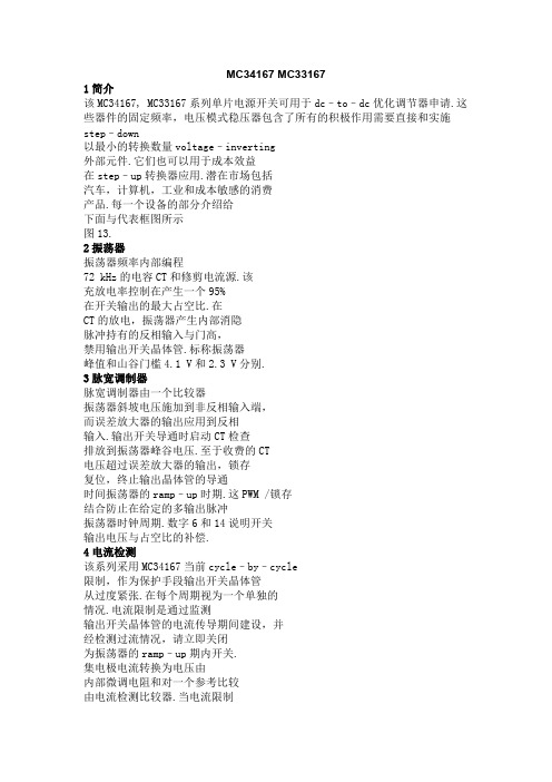
引脚配置
CS
1
SO
2
CNT
3
VBAK
4
X2
5
X1
6
VSS
7
14
是可选的,但如果启用它会断言复位信号为100毫秒,如
果不是由时间窗口内的主机重新启动.一个标志位指示复位源.
每个FM33xx提供非易失性RAM中16Kb的和256Kb的内存容量 .快速的写入速度和无限的耐用性允许的内存来作为 额外的RAM或传统的非易失性存储.这种记忆是真正的非易 失性而非电池供电.
通过一个5位的非易失性设置(寄存器0Ch)60毫秒为增量 .
时基
100毫秒 clock
WR3-0 = 1010b
减计数器
重新启动
/RST
FM33256/FM3316 SPI伴侣W / FRAM
主动一点,如果看门狗达到超时没有被重新启动.如果 发生复位时,定时器将重新启动的复位脉冲的上升沿.如果WDE未启 用,看门狗定时器仍然运行,但对/ RST没有影响.第二个 控件是一个四位的重新启动定时器,从而防止复位.定时 器应改变超时值之后重新启动.
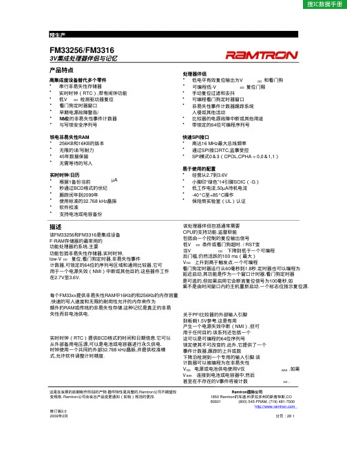
EHV331M16RET3中文资料(HITANO ENTERPRISE)中文数据手册「EasyDatasheet - 矽搜」
WV Cap.
uF 0.47
1 2.2 3.3 4.7 10 22 33 47 100 220 330 470
63
Size 涟
A
5
A
8
A
12
B
17
C
22
C
32
C8
58
E
140
E
170
F
310
G
470
I
650
I
700
100
Size 涟
E
100
F
150
G
250
G
380
I
450
J
590
160
Size 涟
G
电压(V) 6.3
10
16
25
35
50
63 100
160~ 250
400~ 450
尺寸A〜F
0.45 0.35 0.28 0.18 0.16 0.14 0.12 0.12
-
-
尺寸G〜Ĵ
0.45 0.38 0.34 0.26 0.22 0.18 0.14 0.10 0.20
0.25
电压(V)
6.3
10
静电容量变化在 泄漏电流
±25% 初始值(尺寸克〜I: ±20%)
少于 ±300% 指定值(大小为d〜I:
±200%)
比初始规定值以下
存储1000小时,在105后
℃ ,与不施加电压时和稳定在20
℃ ,电容器
应满足负载寿命规定限制.(参考JIS C5101-4 4.1)
尺寸图
SIZE Dφ
LACB
W P±0.2
47
PBT3316泰科纳Ticona物性表

PBT3316泰科纳Ticona物性表PBT3316泰科纳Ticona物性数据表:产品提供久隆塑胶原料tEl134********Celanex3316是一种30%玻璃纤维增强的非渗出性阻燃级(UL和CSA核准的V-0(在1/32英寸时)和5V(在1/16英寸时))聚对苯二甲酸丁二醇酯,其在机械性能和加工性能方面实现了优异平衡。
它非常适合电插座、连接器、电子电气用途。
其中其UL核准的50%再研磨使用能力使得所购买的产品得到最大利用。
熔体体积流动速度,MVR7cm3/10min250℃ 2.16kg ISO1133拉伸模量10700MPa ISO527-1/-2断裂应力135MPa ISO527-1/-2断裂伸长率 2.5%ISO527-1/-2无缺口简支梁冲击强度,+23℃59kJ/m2ISO179/1eU无缺口简支梁冲击强度,-30℃42kJ/m2ISO179/1eU简支梁缺口冲击强度,+23℃8.5kJ/m2ISO179/1eA简支梁缺口冲击强度,-30°C8.5kJ/m2ISO179/1eA熔融温度,10°C/min225℃ISO11357-1/-3热变形温度, 1.80MPa208℃ISO75-1/-2热变形温度,8.00MPa165℃ISO75-1/-2维卡软化温度,50°C/h50N225℃ISO306厚度为h时的燃烧性V-0class测试用试样的厚度0.4mm IEC60695-11-10燃烧性-氧指数30%ISO4589-1/-2介质损耗因子,100Hz33E-4IEC60250介质损耗因子,1MHz145E-4IEC60250体积电阻率1E13Ohm*m IEC60093表面电阻率1E15Ohm IEC60093介电强度34kV/mm IEC60243-1吸水性0.4%类似ISO62吸湿性0.16%类似ISO62密度1660kg/m3ISO1183PBT3316泰科纳Ticona注塑成型参数:为了避免CELANEX树脂在加工过程中发生水解降解,需将其干燥到水分含量等于或小于0.02%。
ESB-33133;中文规格书,Datasheet资料

Note: PP=Self-lock NL=Non-lock
Design and specifications are each subject to change without notice. Ask factory for the current technical specifications before purchase and/or use. Should a safety concern arise regarding this product, please be sure to contact us immediately.
■ Explanation of Part Numbeபைடு நூலகம்s
1 2 3 4 5 6 7 8
E
S
Product Code
B
3
Type
3
Design No.
■ Specifications
Rating Travel Mounting Height Poles and Throws Operating Mode Switching Mode Minimum Quantity/Packing Unit Quantity/Carton 50 µA 3 Vdc to 0.2 A 14 Vdc (Resistive load) Lock travel=1.5 mm Full travel=2.3 mm 6.0 mm 2-poles 2-throws Self-lock, Non-lock Non-shorting 100 pcs. Polyethylene Bag (Bulk) / 300 pcs. Embossed Taping (Reel Pack) 2000 pcs. Polyethylene Bag (Bulk) / 1800 pcs. Embossed Taping (Reel Pack)
RF3336;中文规格书,Datasheet资料

Electrical Characteristics CharacteristicSymNotesMinimumTypical MaximumUnitsCenter Frequency at 25°C Absolute Frequencyf C 1, 2868.225868.475MHz Tolerance from 868.35 MHz∆f C ±125kHz Insertion Loss IL 1 2.65dB 3 dB Bandwidth BW 31,26001000kHz Rejectionat f C- 21.4 MHz (Image)133dBat f C - 10.7 MHz (LO)15Ultimate80TemperatureOperating Case Temp.T C 3, 4-40+85°C Turnover Temperature T O 102540°C Turnover Frequency f O f C MHz Freq. Temp. CoefficientFTC 0.032ppm/°C 2Frequency Aging Absolute Value during the First Year |fA|5≤10ppm/yr External ImpedanceSeries Inductance L 110L 212nH Shunt CapacitanceC 11C 21pFLid Symbolization (in addition to Lot and/or Date Codes)RFM RF3336TO39-3 Case•Ideal Front-End Filter for 868.35 MHz Wireless Receivers •Low-Loss, Coupled-Resonator Quartz Design •Simple External Impedance Matching •Rugged TO39 Hermetic Package•Complies with Directive 2002/95/EC (RoHS)The RF3336 is a low-loss, compact, and economical surface-acoustic-wave (SAW) filter designed to provide front-end selectivity in 868.35 MHz receivers. Receiver designs using this filter include superhet with 10.7MHz or 500kHz IF, direct conversion and superregen. Typical applications of these receivers arewireless remote-control and security devices operating in the USA under FCC Part 15 and in Canada under DoC RSS-210.This coupled-resonator filter (CRF) uses selective null placement to provide suppression, typically greater than 40dB, of the LO and image spurious responses of superhet receivers with 10.7MHz IF. RFM’sadvanced SAW design and fabrication technology is utilized to achieve high performance and very low loss with simple external impedance matching (not included). Quartz construction provides excellent frequency stability over a wide temperature range.868.35 MHzSAW FilterRF3336CAUTION: Electrostatic Sensitive Device. Observe precautions for handling.Notes:1.Unless noted otherwise, all measurements are made with the filter installed in the specified test fixture which is connected to a 50 Ω test system with VSWR ≤ 1.2:1. The test fixture L and C are adjusted for minimum insertion loss at the filter center frequency, f c . Note that insertion loss, bandwidth, and passband shape are dependent on the impedance matching component values and quality. 2.The frequency f c is defined as the midpoint between the 3dB frequencies.3.Unless noted otherwise, specifications apply over the entire specified operating temperature range.4.The turnover temperature, T O , is the temperature of maximum (or turnover) frequency, f o . The nominal frequency at any case temperature, T c , may be calculated from: f =f o [1-FTC (T o -T c )2].5.Frequency aging is the change in fc with time and is specified at +65°C or less. Aging may exceed the specification for prolonged temperatures above +65°C. Typically, aging is greatest the first year after manufacture, decreasing significantly in subsequent years.6.The design, manufacturing process, and specifications of this device are subject to change without notice.7.One or more of the following U.S. Patents apply: 4,54,488, 4,616,197, and others pending.8.All equipment designs utilizing this product must be approved by the appropriate government agency prior to manufacture or sale.PbAbsolute Maximum Ratings Electrical ConnectionsTypical Test CircuitCase DesignRatingValueUnitsIncident RF Power+13dBm DC Voltage Between Any Two Pins (Observe ESD Precautions)±30VDC Case Temperature 5-40 to +85°C Soldering Temperature (10 seconds / 5 cycles max.)260°CPinConnection1Input or Output 2Output or Input 3Case GroundDimensionsMillimeters Inches MinMaxMinMaxA 9.400.370B 3.180.125C 2.503.500.0980.138D 0.46 Nominal 0.018 NominalE 5.08 Nominal 0.200 NominalF 2.54 Nominal 0.100 NominalG 2.54 Nominal0.100 NominalH 1.020.040J1.400.055分销商库存信息: RFMRF3336。
PBS3316-330MT

33
±20% 100kHz
0.100
PBO3316-470MT
47
±20% 100kHz
0.140
PBO3316-680MT
68
±20% 100kHz
0.200
PBO3316-101MT
100
±20% 100kHz
0.280
PBO3316-151MT
150
±20% 100kHz
0.400
PBO3316-221MT
PBS1608-150MT
15
±20%
100kHz
0.260
33
0.80
PBS1608-220MT
22
±20%
100kHz
0.320
25
0.70
PBS1608-330MT
33
±20%
100kHz
0.360
20
0.60
PBS1608-470MT
47
±20%
100kHz
0.450
20
0.50
PBS1608-680MT
SRF
Isat
Irms
(MHz)
(A)
(A)
22
8.0
4.0
20
7.0
3.5
15
5.5
3.0
9
4.5
2.6
8
3.5
2.3
7
3.0
1.8
6
2.6
1.5
5
2.4
1.2
4
1.9
1.0
3
1.4
8.2
2.5
1.2
0.72
2
1.0
3336-52;3336-01;中文规格书,Datasheet资料
©2005-2011 Peregrine Semiconductor Corp. All rights reserved. Page 2 of 13
Document No. 70-0033-05 │ UltraCMOS™ RFIC Solutions
/
PE3336
Product Specification
/
PE3336
Product Specification
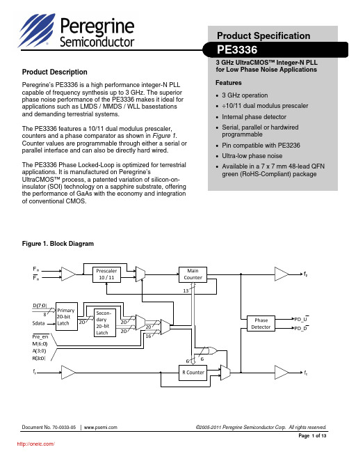
Figure 2. Pin Configurations (Top View)
GND GND GND
48 47 46 45 44 43 42 41 40 39 38 37
D0, M0 D1, M1 D2, M2 D3, M3 VDD VDD S_WR, D4, M4 Sdata, D5, M5 Sclk, D6, M6 FSELS, D7, Pre_en GND FSELP, A0
3 GHz operation ÷10/11 dual modulus prescaler Internal phase detector Serial, parallel or hardwired
programmable
Pin compatible with PE3236 Ultra-low phase noise Available in a 7 x 7 mm 48-lead QFN
Table 1. Pin Descriptions (continued)
Pin No. Pin Name S_WR 7 D4 M4 Sdata 8 D5 M5 Sclk 9 D6 M6 FSELS 10 D7 Pre_en 11 GND FSELP 12 A0 Direct Serial E_WR 13 A1 M2_WR 14 A2 Smode 15 A3 16 17,18 19 20 21 22 Bmode VDD M1_WR A_WR Hop_WR Fin Direct ALL ALL Parallel Parallel Serial, Parallel ALL Input Input (Note 1) Input Input Input Input Direct Serial, Parallel Input Input Parallel Direct Parallel Input Input Input Enhancement register write. D[7:0] are latched into the enhancement register on the rising edge of E_WR. A Counter bit1. M2 write. D[3:0] are latched into the primary register (R[5:4], M[8:7]) on the rising edge of M2_WR. A Counter bit2. Selects serial bus interface mode (Bmode=0, Smode=1) or Parallel Interface Mode (Bmode=0, Smode=0). A Counter bit3 (MSB). Selects direct interface mode (Bmode=1). Power supply input. Input may range from 2.85 V to 3.15 V. Bypassing recommended. M1 write. D[7:0] are latched into the primary register (Pre_en, M[6:0]) on the rising edge of M1_WR. A write. D[7:0] are latched into the primary register (R[3:0], A[3:0]) on the rising edge of A_WR. Hop write. The contents of the primary register are latched into the secondary register on the rising edge of Hop_WR. Prescaler input from the VCO. 3.0 GHz max frequency. ©2005-2011 Peregrine Semiconductor Corp. All rights reserved. Page 3 of 13 Input Input Parallel Direct ALL Parallel Input Input Input Parallel Direct Serial Input Input Input Parallel Direct Serial Parallel Direct Serial Input Input Input Input Input Input Interface Mode Serial Type Input Description Serial load enable input. While S_WR is “low”, Sdata can be serially clocked. Primary register data are transferred to the secondary register on S_WR or Hop_WR rising edge. Parallel data bus bit4 M Counter bit4 Binary serial data input. Input data entered MSB first. Parallel data bus bit5. M Counter bit5. Serial clock input. Sdata is clocked serially into the 20-bit primary register (E_WR “low”) or the 8-bit enhancement register (E_WR “high”) on the rising edge of Sclk. Parallel data bus bit6. M Counter bit6. Selects contents of primary register (FSELS=1) or secondary register (FSELS=0) for programming of internal counters while in Serial Interface Mode. Parallel data bus bit7 (MSB). Prescaler enable, active “low”. When “high”, Fin bypasses the prescaler. Ground. Selects contents of primary register (FSELP=1) or secondary register (FSELP=0) for programming of internal counters while in Parallel Interface Mode. A Counter bit0 (LSB). Enhancement register write enable. While E_WR is “high”, Sdata can be serially clocked into the enhancement register on the rising edge of Sclk.