FSS_Guide
频率选择表面的等效电路_概述说明以及解释

频率选择表面的等效电路概述说明以及解释1. 引言1.1 概述频率选择表面(Frequency Selective Surface,简称FSS)是一种具有特定频率响应特性的二维或三维结构,常用于控制电磁波的传输和反射。
相比于传统的无源电子元件,频率选择表面通过其特殊的等效电路模型实现了对电磁波的频率选择功能。
本文将介绍频率选择表面的等效电路模型以及其在通信、雷达、天线等应用领域中的重要性。
1.2 文章结构本文主要包括以下几个部分:引言、频率选择表面的等效电路概述、频率选择表面的等效电路模型、设计和优化方法、结论与展望。
首先,我们将在引言部分介绍文章的背景和目的,为后续内容做铺垫。
接着,我们将详细阐述频率选择表面的定义和背景,并探讨其结构和原理以及在不同应用领域中的应用情况。
然后,我们将介绍常见的几种频率选择表面的等效电路模型,包括电感模型、电容模型和电阻模型。
随后,我们将探讨设计和优化方法,涵盖参数选择与调整、材料特性与性能分析以及实验测试与验证技术。
最后,我们将总结主要发现,并展望频率选择表面的未来发展方向。
1.3 目的本文旨在深入了解频率选择表面的等效电路模型,包括其定义和背景、结构和原理以及应用领域。
通过对电感模型、电容模型和电阻模型的介绍,读者可以对频率选择表面的工作原理有更为清晰的认识。
同时,我们将讨论设计和优化方法,以帮助读者更好地应用频率选择表面于实际工程中。
最后,我们将总结文章主要内容,并探讨未来频率选择表面在相关领域中的潜在发展方向。
2. 频率选择表面的等效电路2.1 定义和背景频率选择表面(Frequency Selective Surface,简称FSS)是一种具有特定波长选择性的电磁波滤波结构。
它可以实现对特定频率范围内的电磁波进行选择性透射或反射。
在无线通信系统、天线设计、雷达技术、光学器件等领域,对特定频段的电磁波进行控制和管理是非常重要的。
频率选择表面通过其特殊的物理结构和材料参数,能够实现对特定频率范围内电磁波的限制或传输,在这些应用中得到了广泛的应用。
通航飞行服务站(FSS)
通航飞⾏服务站(FSS)飞⾏服务站(FSS)可为通⽤航空飞⾏及时提供飞⾏计划服务、⽓象服务、情报服务、告警服务、飞⾏⽀援、应急救援和其他相关⽀持的空中交通服务。
FSS起源于通⽤航空发达的美国。
美国⽬前约有180个FSS和58个⾃动FSS,与之相⽐,我国的通⽤航空活动规模⼩,FSS建设相对滞后。
随着我国推⾏低空空域管理改⾰,2013年海南东⽅、深圳南投、珠海、沈阳法库4个FSS试点相继落成。
⽬前,我国已建及在建的FSS共10个。
服务流程和作⽤FSS为通⽤航空⽤户在飞⾏活动过程中提供的服务包括飞⾏前、飞⾏中和飞⾏后三个阶段。
在各阶段,FSS提供的服务类型是不同的。
飞⾏前服务,包括飞⾏前讲解和飞⾏计划的申报。
⾏前讲解主要提供⽓象信息、航空情报信息和对飞⾏计划的建议。
FSS通过与军民航管制部门、⽓象部门、情报部门的联系,可以获取本地区的⽓象信息以及情报信息,同时能够上报通航⽤户申报的飞⾏计划。
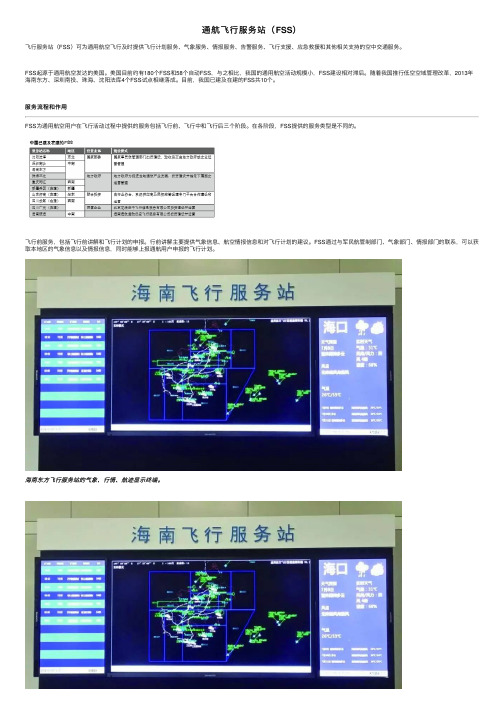
海南东⽅飞⾏服务站的⽓象、⾏情、航迹显⽰终端。
海航通航飞⾏监视服务系统。
飞⾏中服务,包括飞⾏中讲解和飞⾏情报服务,飞⾏员空中报告,低空通信服务,对空监视服务,告警和救援服务,飞⾏计划实施报告。
FSS通过低空空域对空监视和低空通信系统中的监视/通信中⼼站,可以获取本地区的监视信息,同时能够为通航⽤户或通航机场等提供通信服务、告警及救援服务。
此外,FSS能够与区域级的FSS进⾏信息共享,把本站收集到的⽓象信息、情报信息、监视信息、告警及救援信息、飞⾏活动统计、飞⾏计划实施情况等上传到区域级的FSS进⾏汇总。
同时,FSS也能够从区域级的FSS获取到更⼤范围的⽓象信息、情报信息、监视信息,为通航⽤户或通航机场提供更全⾯、更⼴泛的服务。
飞⾏后服务,包括飞⾏员报告,飞⾏活动统计和飞⾏计划完成报告。
飞⾏员报告包括飞⾏后通⽤导航设施报告和飞⾏后⽓象报告。
飞⾏后通⽤导航设施报告是通⽤航空⽤户飞⾏后对通⽤导航设施⼯作状态的报告;飞⾏后⽓象报告是通⽤航空⽤户提供航线、活动区域内相关天⽓的报告。
FSSmart操作手册

FSSmart 操作手册; 19.07.09; 14:13ISRA VISION LASOR GMBHRudolf-Diesel-Str. 24D-33813 OerlinghausenGermanyTel.: +49/5202/708-0Fax: +49/5202/708-130Email: info@Internet: 浙玻平湖有限公司Floatscan Smart206958操作指导目录1概述 (4)1.1介绍 (4)1.2设备型号、编号、制造年份 (6)1.3制造商、服务地址 (6)1.4关于作者和知识产权的说明 (6)1.5操作员指导 (6)1.6指导和培训协助 (6)1.7规定用途 (7)2安全规定 (8)2.1一般性安全规定 (8)2.2设备管理人员责任 (8)2.3调试的安全规范 (9)2.4操作的安全规范 (9)2.5维护、保养和故障排除的安全规范 (11)2.6关于电源的安全规范 (12)2.7LED光源的安全规范 (13)2.8设备的结构修改 (13)2.9残存危险 (14)3责任、质量保证 (14)4空调设备的噪音水平 (14)5FLOATSCAN SMART的功能描述 (15)6操作 (16)6.1启动/关闭 (16)6.1.2关闭设备上的计算机 (16)6.1.3用户权限/用户选择 (16)6.1.4启动程序 (16)6.2D OT M AP (17)6.3C LIENT A REA (18)6.4S YSTEM I NFO (19)6.5选择显示的数据和时间段 (20)6.6O PERATOR (21)6.6.1激活产品 (21)6.7S POT IMAGES (22)6.8S POT S TATISTICS (23)6.8.1配置 (24)6.8.2图形 (26)26.9O PTICS M AP (29)6.10S POT M AP (31)6.11D EFECT L IST (33)6.12O PTICS L IST (35)6.13P LATE PROTOCOL (36)6.14P ARAMETER EDITOR (37)6.14.1分级过程 (37)6.14.2Logo (37)6.14.3COP (优化切割) (38)6.14.4ROI (38)6.14.5Sensitivity (Sens.) (38)6.14.6Deformation (Size CLS) (38)6.14.7Core (38)7维护 (38)7.1清理指导 (38)7.1.1一般性清理指导 (38)7.2维护间隔 (39)7.2.1清理光源窗 (39)7.2.2清理照相机盖 (39)7.2.3清理照相机镜头 (39)8技术数据 (40)31 概述1.1 介绍本操作指导手册提供了成功和安全地操作Floatscan Smart的基本帮助。
CST仿真FSS详细步骤
CST仿真FSS详细步骤1.设计FSS的结构:确定FSS的材料、尺寸和形状。
根据需要的频率选择特性,选择合适的介质常数和介质厚度。
然后,在CST软件中创建新的电磁场模型。
2.确定工作频率范围:确定FSS需要工作的频率范围。
根据这个频率范围选择一个适当的频率步长,这将会在后续的仿真中使用到。
3.创建基本单元单元:将单元格的尺寸设置为工作频率的一半。
然后,在CST软件中创建一个新的结构,进行基本单元单元的布局。
可以使用基本几何形状,如方形、圆形等。
根据需求,可以在基本单元单元中添加细微的调整和微调。
4.定义边界条件:使用波导端口或离散端口定义边界条件。
根据CST软件的版本,选择适当的方法。
为了更好地控制射频传输效率和能量流动,可以对单元进行调整。
5.运行频率域仿真:在CST软件中设置频率范围并运行频率域仿真。
CST将计算相应频率下的散射参数,并提供图表和图像显示。
6.优化FSS性能:根据仿真结果,对FSS的结构进行调整和优化。
可以修改单元的尺寸、形状和布局,以获得所需的传输/反射系数。
7.进行时域仿真:完成频率域仿真后,可以选择进行时域仿真,以确定FSS在不同时间步骤中的行为。
时域仿真可以提供更详细的传输和反射特性。
8.分析结果:根据时域仿真结果,分析FSS的频率选择特性和波传输效果。
根据需要,可以通过调整FSS的结构进一步优化性能。
9.导出结果:根据模型的需求,导出结果数据。
可以导出图表、图像和参数数据。
10.进行实验验证:根据仿真结果设计和制作实际的FSS样品,并进行实验验证。
根据实际测量数据,对FSS进行进一步优化和调整。
以上是CST仿真FSS的详细步骤,通过反复优化和调整,可以设计出满足特定频率选择特性的FSS结构。
汽车法规--ISO9141-2的国际标准文档4(pdf 58)

SSF 14230Road Vehicles - Diagnostic SystemsKeyword Protocol 2000 - Part 2 - Data Link LayerSwedish Implementation StandardBased on ISO 14230-2 Data Link LayerStatus:Issue 1Date: April 22, 1997This document is based on the InternationalStandard ISO 14230 Keyword Protocol 2000 andhas been further developed to meet Swedishautomotive manufacturer's requirements by theSwedish Vehicle Diagnostics Task Force.It is based on mutual agreement between thefollowing companies:•Saab Automobile AB•SCANIA AB•Volvo Car Corp.•Volvo Bus Corp.•Mecel ABFile: 14230-2s.DOC / Definition by “Samarbetsgruppen för Svensk Fordonsdiagnos” / Author: L. Magnusson Mecel ABDocument updates and issue historyThis document can be revised and appear in several versions. The document will be classified in order to allow identification of updates and versions.A. Document status classificationThe document is assigned the status Outline, Draft or Issue.It will have the Outline status during the initial phase when parts of the document are not yet written.The Draft status is entered when a complete document is ready, which can be submitted for reviews. The draft is not approved. The draft status can appear between issues, and will in that case be indicated together with the new issue number E.g. Draft Issue 2.An Issue is established when the document is reviewed, corrected and approved.B. Version number and history procedureEach issue is given a number and a date. A history record shall be kept over all issues.Document in Outline and Draft status may also have a history record.C. HistoryIssue #Date Comment197 04 22Frst issueTable of Content1. SCOPE (1)2. NORMATIVE REFERENCE (2)3. PHYSICAL TOPOLOGY (3)4. MESSAGE STRUCTURE (4)4.1 Header (4)4.1.1 Format byte (4)4.1.2 Target address byte (5)4.1.2.1 Physical addressing (5)4.1.2.2 Functional addressing (5)4.1.3 Source address byte (5)4.1.4 Length byte (5)4.1.5 Use of header bytes (6)4.2 Data Bytes (6)4.3 Checksum Byte (6)4.4 Timing (7)4.4.1 Timing Exceptions (9)4.4.2 Periodic transmission (9)4.4.3 Server (ECU) Response Data Segmentation (12)4.5 End Of Message (12)5. COMMUNICATION SERVICES (13)5.1 StartCommunication Service (14)5.1.1 Service Definition (14)5.1.1.1 Service Purpose (14)5.1.1.2 Service Table (14)5.1.1.3 Service Procedure (14)5.1.2 Implementation (14)5.1.2.1 Key bytes (15)5.1.2.2 Fast Initialisation (17)5.2 StopCommunication Service (19)5.2.1 Service Definition (19)5.2.1.1 Service Purpose (19)5.2.1.2 Service Table (19)5.2.1.3 Service Procedure (19)5.2.2 Implementation (20)5.3 AccessTimingParameter Service (21)5.3.1 Service Definition (21)5.3.1.1 Service Purpose (21)5.3.1.2 Service Table (21)5.3.1.3 Service Procedure (22)5.3.2 Implementation (23)5.4 SendData Service (25)5.4.1 Service Definition (25)5.4.1.1 Service Purpose (25)5.4.1.2 Service Table (25)5.4.1.3 Service Procedure (25)5.4.2 Implementation (26)6. ERROR HANDLING (27)6.1 Error handling during physical/functional Fast Initialisation (27)6.1.1 Client (tester) Error Handling during physical/functional Fast Initialisation (27)6.1.2 Server (ECU) Error Handling during physical Fast Initialisation (27)6.1.3 Server (ECU) Error Handling during functional Fast Initialisation (28)6.2 Error handling after Initialisation (28)6.2.1 Client (tester) communication Error Handling (28)6.2.2 Server (ECU) communication Error Handling. physical addressing (29)6.2.3 Server (ECU) Error Handling, functional addressing (29)APPENDIX A - ARBITRATION1. DEFINITIONS (1)1.1 Random response time (1)1.2 Start bit detection (1)1.3 Transmission latency (1)1.4 Collision detection (1)2. MAINSTREAM COMMUNICATION (1)APPENDIX B - TIMING DIAGRAMS1. PHYSICAL ADDRESSING (1)1.1 Physical addressing - single positive response message (1)1.2 Physical addressing - more than one positive response message (3)1.3 Physical addressing - periodic transmission (5)2. FUNCTIONAL ADDRESSING (7)2.1 Functional addressing - single positive response message -single server (ECU) addressed (7)2.2 Functional addressing - more than one response message -single server (ECU) addressed (9)2.3 Functional addressing - single positive response message -more than one server (ECU) (11)2.4 Functional addressing - more than one response message -more than one server (ECU) (13)APPENDIX C - MESSAGE FLOW EXAMPLES1. PHYSICAL INITIALISATION - MORE THAN ONE SERVER (ECU) INITIALISED (1)2. PERIODIC TRANSMISSION MODE (4)2.1 Message Flow Example A (4)2.2 Message Flow Example B (5)IntroductionThis document (The Swedish Keyword Protocol 2000 Implementation Standard) is based on the ISO 14230-2 International Standard. Changes are indicated by changing the font from "Arial" to "Times New Roman"!It has been established in order to define common requirements for the implementation of diagnostic services for diagnostic systems.To achieve this, the standard is based on the Open System Interconnection (O:S:I.) Basic Reference Model in accordance with ISO 7498 which structures communication systems into seven layers. When mapped on this model, the services used by a diagnostic tester and an Electronic Control Unit (ECU) are broken into:- Diagnostic services (layer 7)- Communication services (layers 1 to 6)See figure 1 below.1. ScopeThis national Standard specifies common requirements of diagnostic services which allow a tester to control diagnostic functions in an on-vehicle Electronic Control Unit (e.g. electronic fuel injection, automatic gear box, anti-lock braking system,...) connected on a serial data link embedded in a road vehicle.It specifies only layer 2 (data link layer). Included are all definitions which are necessary to implement the services (described in "Keyword Protocol 2000 - Part 3:Implementation) on a serial link (described in "Keyword Protocol 2000 - Part 1: Physical Layer") Also included are some communication services which are needed for communication/session management and a description of error handling.This Standard does not specify the requirements for the implementation of diagnostic services.The physical layer may be used as a multi-user-bus, so a kind of arbitration or bus management is necessary. If arbitration is used it shall comply to the technique described in Attachment A. The car manufacturers are responsible for the correct working of bus management.Communication between ECUs are not part of this document.The vehicle diagnostic architecture of this standard applies to:• a single tester that may be temporarily or permanently connected to the on-vehicle diagnostic data link and• several on-vehicle electronic control units connected directly or indirectlySee figure 2 below.2. Normative ReferenceThe following standards contain provisions which, through reference in this text, constitute provisions of this document. All standards are subject to revision, and parties to agreement based on this document are encouraged to investigate the possibility of applying the most recent editions of the standards listed below. Members of ISO maintain registers of currently valid International Standards.ISO 7498-1:1984Information processing systems - Open systemsinterconnection - Basic reference model.SAE J-1979:Dec,1991E/E Diagnostic Test ModesSAEJ-2178 :June, 1993Class B Data Communication Network MessagesISO 14229:1996Road Vehicles - Diagnostic systems -Diagnostic Services SpecificationSSF 14230-1:1997Road Vehicles - Diagnostic systems - Keyword Protocol 2000 -Issue 2Part 1: Physical LayerSSF 14230-3:1996Road Vehicles - Diagnostic systems - Keyword Protocol 2000 -Draft Part 3: ImplementationISO 14230-4:1996Road Vehicles - Diagnostic systems - Keyword Protocol 2000 -Part 4: Requirements For Emission related Systems3. Physical topologyKeyword Protocol 2000 is a bus concept (s. diagram below). Figure 3 shows the general form of this serial link.Figure 3 - TopologyThe K-Line is used for communication and initialisation. Special cases are node-to-node-connections, that means there is only one ECU on the line, which also can be a bus converter.4. Message structureThis section describes the structure of a message.The message structure consists of three parts:• header• data bytes• checksumHeader Data bytes ChecksumFmt Tgt1 Src1 Len1SId2 . .Data2 . . CSmax . 4 byte max. 255 byte 1 byte1 bytes are optional, depending on format byte2 Service Identification, part of data bytesHeader and Checksum byte are described in this document. The area of data bytes always begins with a Service Identification. Use of the data bytes for communication services is described in this document. Use of the data bytes for diagnostic services is described in "Keyword Protocol 2000 - Part 3: Implementation".4.1 HeaderThe header consists of 3 or 4 bytes. A format byte includes information about the form of the message. A separate length byte allows message lengths up to 255 bytes.4.1.1 Format byteThe format byte contains 6 bit length information and 2 bit address mode information. The tester is informed about use of header bytes by the key bytes (s.5.1.2.1).msb lsbA1A0L5L4L3L2L1L0• A1,A0: Define the form of the header which will be used by the message:A1A0Mode Mnemonic HeaderMode210Header with address information, physical target address HM2 311Header with address information, functional target address HM3HM0 and HM1 are not defined in this document.HM3 (functional target address) shall only be used in request messages see §5.1.2.2.2• L5..L0: Define the length of the data field of a message, i.e. from the beginning of the data field (Service Identification byte included) to Checksum byte (not included). A message length of 1 to 63 bytes is possible. If L0 to L5 = 0 then the additional length byte is included.In the Swedish Implementation Standard L0 to L5 shall always be set to 0 (except in theStartCommunicationRequest message, see §5.1.2.2).This is the target address for the message. It may be a physical or a functional address. For emission related (CARB) messages this byte is defined in ISO 14230 KWP 2000 Part 4: Requirements For Emission related Systems.4.1.2.1 Physical addressingPhysical addressing (HM2) can be used in both request and response messages. The target address of a physically addressed request shall be interpreted as a physical server (ECU) address, the source address is the physical address of the client (tester).In the response message the target and source addresses are also physical addresses (HM2). Physical addresses shall be according to SAE J2178-Part 1, or as specified by the vehicle manufacturer.4.1.2.2 Functional addressingFunctional addressing (HM3) can only be used in request messages. The target address of a functionally addressed request shall be interpreted as a functional (group) address, the source address is the physical address of the client (tester).In the response messages the target and source addresses are physical addresses, i.e. response messages are always physically addressed (HM2).Functional addressing requires that the servers (ECUs) must support arbitration (see appendix A).4.1.3 Source address byteThis is the address of the transmitting device. It must be a physical address (also in the case where the target address is a functional address). There are the same possibilities for the values as described for physical target address bytes. Addresses for testers are listed in SAE J2178 Part 1, but the ECU must accept all tester addresses.4.1.4 Length byteThis byte is provided if the length in the header byte (L0 to L5) is set to 0. It allows the user to transmit messages with data fields longer then 63 bytes. With shorter messages it may be omitted. This byte defines the length of the data field of a message, i.e. from the beginning of the data field (Service Identification byte included) to Checksum byte (not included). A data length of 1 to 255 bytes is possible. The longest message consists of a maximum of 260 byte (255 data bytes + 4 bytes header + Checksum). For messages with data fields of less than 64 bytes there are two possibilities: Length may be included in the format byte or in the additional length byte. An ECU may support both possibilities, the tester is informed about this capability through the keybytes ( see section 5.1.2.1).Length Length provided inFmt byte Length byte< 64XX00 0000present< 64XXLL LLLL not present≥ 64XX00 0000presentXX: 2 bit address mode information (see §4.1.1)LL LLLL: 6 bit length informationIn the Swedish Implementation Standard the Length byte shall always be provided (L0 to L5 = 0) (except in the StartCommunicationRequest message, see §5.1.2.2).With the above definitions there are two different forms of message. These are shown diagramatically below.LengthFmt Tgt Src SId Data CSChecksumHeader with address information, no additional length byteLengthFmt Tgt Src Len SId Data CSChecksumHeader with address information, with additional length byteFmt Format byteTgt Target addressSrc Source addressLen additional length byteSId Service Identification byteData depending on serviceCS Checksum byte4.2 Data BytesThe data field may contain up to 255 bytes of information. The first byte of the data field is the Service Identification Byte. It may be followed by parameters and data depending on the selected service. These bytes are defined in "Keyword Protocol 2000 - Part 3: -Implementation" (for diagnostic services) and in section 5 of this document (for communication services).4.3 Checksum ByteThe Checksum byte (CS) inserted at the end of the message block is defined as the simple 8-bit sum series of all bytes in the message, excluding the Checksum.If the message is<1> <2> <3> ... <N> , <CS>where <i> (1 ≤ i ≤ N) is the numeric value of the i th byte of the message, then:<CS> = <CS>Nwhere <CS>i (i = 2 to N) is defined as<CS>i = { <CS> i-1 + <i> } Modulo 256 and <CS>1 = <1>Additional security may be included in the data field as defined by the manufacturer.4.4 TimingDuring normal operation the following timing parameters are relevant:Value DescriptionP1Inter byte time in ECU response.P2Time between end of tester request and start of ECU response, or time between end of ECU response and start of next ECU response.The next ECU response may be from the same ECU or it may be from another ECUin case of functional addressing.P3Time between end of ECU response and start of new tester request, or time between end of tester request and start of new tester request if ECU fails torespond.P3 shall be measured from the last byte in the latest response message from anyECU responding.P4Inter byte time in tester request.There are two sets of default timing parameters, normal and extended. Only normal timing parameters are supported by this document (Swedish Implementation Standard).Table 1a shows the timing parameters which are used as default (all values in ms).Table 1a - Normal Timing Parameter Set, default valuesTiming min. values max. valuesParameter default defaultP1020P2 P2*2525505000P3555000P4520Note: The timing parameter P2* becomes active if the server (ECU) responds with Negative response and the response code $78 "reqCorrectlyRcvd-RspPending", see §4.4.1.The values of the timing parameters may be changed with the communication service "AccessTimingParameters" (see §5.3).Table 1b shows the resolution and the possible limits within which the timing parameters can be changed with AccessTimingParameters (ATP).Table 1b -Normal Timing Parameter Set, lower and upper limitsAll values in msTiming Min. values Max. valuesParameter Lower limit Resolution 1Upper limit Resolution 1P10---20---P200.589600 ; ∞see Table 1cP300.563500∞250 see note 2P400.520---1) Min./Max. value calculation method [ms] = ATP parameter value * Resolution2) ATP parameter value = $FF => Max. value = ∞Table 1c - P2max Timing Parameter calculationTiming Parameter Hex valueof ATPparamete rResolutionin [ms]valuein [ms]Maximum value calculation methodin [ms]P2max01 to F02525 to 6000(hex value) - (Resolution) F1F2F3F4F5F6 F7 F8 F9 FA FB FC FD FE see maximumvaluecalculationmethod640012800192002560032000384004480051200576006400070400768008320089600(low nibble of hex value) - 256 - 25Example of $FA:($0A - $0100) - 25 = 64000FF---∞= ∞The P2max timing parameter calculation uses 25 [ms] resolution in the range of $01 to $F0.Beginning with $F1 a different calculation method shall be used by the server and the client in order to reach P2max timing values greater than 6000 [ms].Calculation Formula for P2max values > $F0Calculation_Of_P2max [ms] = (low nibble of ATP parameter P2max) * 256 * 25Note:The P2max timing parameter value shall always be a single byte value in the AccessTimingParameter service. The timing modifications shall be activated by implementation of the AccessTimingParameter service.Users must take care for limits listed above and the following restrictions:P3min > P2max(to avoid collisions in case of func. addressing or data segm.)P3min > P4min(to guarantee that the ECU can receive the first byte)Pimin < Pimax for i=1,...,4When the tester and listening ECUs detect the end of a message by time-out, the following restrictions are also valid:P2min > P4maxP2min > P1maxIt is in the system designers responsibility to ensure proper communication in the case of changing the timing parameters from the default values.He also has to make sure that the chosen communication parameters are possible for all ECUs which participate in the session.The possible values depend on the capabilities of the ECU. In some cases the ECU possibly needs to leave its normal operation mode for switching over to a session with different communication parameters.For complete timing diagrams see appendix B.4.4.1 Timing ExceptionsThe extended P2 timing window is a possibility for (a) server(s) to extend the time to respond on a request message. A timing exception is only allowed with the use of one or multiple negative response message(s) with response code $78 (requestCorrectlyReceived-ResponsePending) by the server(s). This response code shall only be used by a server in case it cannot send a positive or negative response message based on the client's request message within the active P2 timing window.After the transmission of the first negative response message, with response code $78, from the server (ECU) the timing parameter P2* becomes active, instead of the original timing parameter P2, in both the server and the client.The timing parameter P2* shall be generated as described in the following formula: P2*min = P2minP2*max = P3maxThe server(s) shall send multiple negative response messages with the negative response code $78 if required.As soon as the server has completed the task (routine) initiated by the request message it shall send either a positive or negative response message (with a response code other than $78) based on the last request message received. When the client has received the response message, which has been preceded by the negative response message(s) with response code $78, the timing parameter P2 becomes active again in both the server and the client. The client shall not repeat the request message after the reception of a negative response message with response code $78.4.4.2Periodic transmissionThe Keyword Protocol 2000 Periodic Transmission Mode shall be enabled by starting a diagnostic session with the startDiagnosticSession service and the diagnosticMode (DCM_) parameter set to $82 for PeriodicTransmission.PeriodicTransmission shall be supported in connection with physical addressing, normal and modified timing. The description below explains in steps how the PeriodicTransmission mode shall be activated, handled and de-activated.Step #1:To enable the PeriodicTransmission mode in the client (tester) and the server (ECU) the client (tester) shall transmit a startDiagnosticSession request message containing thediagnosticMode parameter for the PeriodicTransmission. After the reception of the firstpositive response message from the server (ECU) the PeriodicTransmission mode isenabled and periodic transmission mode communication structure and timing becomesactive. From now on, the server (ECU) shall periodically transmit the last responsemessage with current (updated, if available) data content, until the client (tester) sends arequest message within the timing window P3*. The timing parameters can be changedwithin the possible limits of the periodic transmission timing parameter set (see Table1d) with the communication service AccessTimingParameters.Step #2:After reception of any request message within the timing window P3*, the server (ECU) shall periodically transmit the corresponding response message which can be either apositive or a negative response message.Step #3:After reception of a stopDiagnosticSession or stopCommunication request message within the timing window P3*, the server (ECU) shall transmit the correspondingpositive response message only once.After reception of a stopDiagnosticSession or stopComunication positive responsemessage the periodicTransmissionMode is disabled and the default diagnostic sessionwith the default timing values, defined by the key bytes becomes active.After reception of a stopDiagnosticSession or stopComunication negative responsemessage the periodicTransmissionMode shall continue. In such case the server (ECU)shall transmit negative response messages unless the client (tester) sends a new requestmessage within the timing window P3*.During the standardDiagnosticModeWithPeriodicTransmission the following rules have to be considered:1.The client (tester) has to ignore the original timing window P3 and shall generate a new timingparameter for the jump-in timing window, which is called from now on P3*.The timing parameter P3* shall be generated as described in the following formula:P3*max = P2min - 2 msP3*min = P3minNote: The original P3max timing parameter is only used for time out detection during negative response message handling with the response code $78 "reqCorrectlyRcvd-RspPending".2.The timing window P3*, which starts at P3*min and ends at P3*max, shall be at least 5ms. It isimportant for the client (tester) to guarantee a minimum size of the jump-in window for the start of a request message.3.The timing window P3* starts and ends before the timing window P2 starts.4.P1max shall not exceed P2min. This is required in order to support resynchronisation betweenthe server (ECU) and client (tester) to meet the error handling requirements.5.Default and optimised timing parameter valuesThe timing table below specifies the timing parameter values with the diagnostic mode standardDiagnosticModeWithPeriodicTransmission.Table 1d -Timing parameter - periodic transmission.All values in msTiming minimum values maximum valuesParameter lower limit default resolution 1default upper limit resolution 1 P100---20200.5P27250.55089600; ∞see Table 1cP2* 37250.5500063500∞250 see note 2P3050.5500063500∞250 see note 2P3* 4050.523125.50.5P4050.520200.51) Min./Max. value calculation method [ms] = ATP parameter value * Resolution2) ATP parameter value = $FF => Max. value = ∞3) The timing parameter P2* becomes active if the server (ECU) responds with Negative response and the response code $78 "reqCorrectlyRcvd-RspPending", see §4.4.14) The timing parameter P3* can be changed, indirectly, by changing the timing parameters P2 and P3 with the service “AccessTimingParameters”.6.When implementing the standardDiagnosticModeWithPeriodicTransmission the followinglimits and restrictions must be considered as listed below:•Pimin < Pimax for i=1, ,4•P1max < P2min•P3min ≤ P2min - 10msIt is the system designers responsibility to ensure proper communication in the case of changing the timing parameters from their default values.It is also the system designers responsibility to ensure proper communication when periodic transmission is used in combination with multiple diagnose, see §5.1.2.2.For complete timing diagrams and message flow examples see appendix B and C.4.4.3Server (ECU) Response Data SegmentationServer (ECU) Response Data Segmentation is used if a client (tester) has sent a request message which causes the server (ECU) to split the response message content (data bytes) into several data segments. The data segments shall be transmitted consecutively in repeated response messages. Each message shall be transmitted within the timing window P2. The data field of each response message shall consist of the Service ID and the corresponding data segment (see figure 5).Data segmentation shall be detected by the client (tester) by comparing source addresses and Service IDs which must be identical for all response messages during segmentation.Server (ECU) response data segmentation shall only be used when the data length exceeds the maximum length that the server (ECU) can transmit in a single message. Data segmentation shall not be supported in periodic transmission mode.This procedure shall also be used to meet the requirements of ISO 14230-4 Keyword Protocol 2000 - Part 4: Requirements For Emission Related Systems.If data segmentation is used the following restriction shall apply:P3min > P2max4.5End Of MessageThe end of a received message shall be detected as:Number of bytes received equals message length (as defined in the format byte or length byte) orTime-out of inter byte time in the received message (P1max exceeded in ECU transmission, P4max exceeded in tester transmission)whichever occurs first.5. Communication servicesSome services are necessary to establish and maintain communication. They are not diagnostic services because they do not appear on the application layer. They are described in the formal way and with the conventions defined in ISO/WD 14229, i.e. a definition of the service purpose, a service table and a verbal description of the service procedure. A description of implementation on the physical layer of Keyword Protocol 2000 is added.The StartCommunication Service and the AccessTimingParameters Service are used for starting a diagnostic communication. In order to perform any diagnostic service, communication must be initialised and the communication parameters need to be appropriate to the desired diagnostic mode. A chart describing this is shown in figure 6.Figure 6 - Use of communication services。
项目4_4.1国际海上人命安全公约.
轮机工程系
船舶管理
任务一 国际海上人命安全公约
能力目标:通过学习国际上有关船舶营运安全的公约和
规则,提高高级轮机人员的安全意识和管理水平,切实做到 遵纪守法,按章操作,自觉地维护和遵守国际海上交通秩序, 保证航行安全。
学习任务:1、识记国际海上人命安全公约的主要内容
2、识记国际消防系统安全规则(FSS规则)的主要内容 3、识记国际救生设备规则(LSA规则)的主要内容 4、识记国际安全管理规则(ISM规则)的主要内容 5、识记国际船舶和港口设施保安规则(ISPS规则)的主要内容
的缔约国,在该修正案通过之后没有对其内容提出任何反 对意见,因此,该规则对我国具有约束力。
江苏海事职业技术学院学院
轮机工程系
国际通岸接头
船舶管理
国际通岸接头
江苏海事职业技术学院学院
轮机工程系
船舶管理
紧急脱险呼吸装置(EEBD)
江苏海事职业技术学院学院
轮机工程系
船舶管理
国际海上人命安全公约
三、国际救生设备规则 LIFE-SAVING APPLIANCE (LSA)
• 除另有明文规定外,本章适用于本规则所适用的所有船 舶和300总吨及以上的货船。
江苏海事职业技术学院学院
轮机工程系
船舶管理
国际海上人命安全公约
8.第Ⅶ章危险货物装运
• 本章包括了包装形式、散装固体形式、散装化学液体和液 化气体危险货物的分类、包装、标志和积载的条款,其内 容分为A,B,C,D四个部分:
江苏海事职业技术学院学院
轮机工程系
船舶管理
国际海上人命安全公约产生背景
江苏海事职业技术学院学院
轮机工程系
船舶管理
FSS自由曲面设计
在3D空间做曲线: 1- 定义主平面 2- 创建
创建的类型:
Through points: 通过每一个点; Control points: 所做的点是控制点 Near points: 线的类型不同
• 如果任选点,曲线将位于定义平面上 • 如果选已经存在的点,那么将产生空间曲线 • 如果需要的不是上述情况 ,激活Disable geometry
似于Loft
步骤: 1- 选 profile 2- 选 Spine 3- 选 Guide
注意:
-所有元素必须是互 相接触的
江达公司
• Translation: profile 沿 spine 轮廓转换 • On contour: profile 位于轮廓三面体 (T, N, B) • Fixed direction: 定义方向
效果图 测量数据
FSS创建曲面
FSK
FSS创建曲面
GSD详细设计
DSE
QSR
真实渲染
FSS创建曲面
GSD详细设计
验证、 修改
GSD详细设计
使用其它 模块完成
江达公司
23
CATIA 介绍
FreeStyle Sketch Tracer
江达公司
24
调入一个图片
江达公司
25
确定图的位置、比例
江达公司
26
显示曲面特性。
10
Blend
Blend 曲线
Blend :做出一条新曲线 连接两条曲线,并定义连接方式 1- 选一条曲线 2- 第二条 3- 定义连接类型
接触点: 显示接触点 (dashboard). 并可以调整接触点
连续值: 显示 (dashboard)并调整
FSS-自由曲面设计PPT课件
3D curve
创建关联的 3D 曲线,这意味着在创建或编辑时可以添加或删除点(控制点或穿越点)。 A:创建关联的 3D 曲线的三种方式: 1.通过点 (Through points):结果曲线为一条通过每个选定点的多弧曲线 2.控制点 (Control points):所单击的点为结果曲线的控制点 3.近似点 (Near points):结果曲线为一条具有固定度数并平滑通过选定点的单弧 B: more frame
将曲线投影到曲面上 选线 + ctrl + 选面
19
Creating Blend Curves
创建混合/桥接曲线 1.选线 2.上下文选项
20
Styling corner
在其它两个平面曲线之间的给定半径连接曲线
21
Matching Curves
曲线匹配 需要两个元素 1.曲线(匹配时变形,与第二个元素匹配) 2.曲线/曲线上的点/3D点/端点 选点就近匹配原则
• 重新回到 xyz 模式--------------------------------------------------------------
• 坐标与实体链接转换-----------------------------------------------------------
• 如果与实体链接, 创建一个坐标平面 -------------------------------------------
15
Creating a Styling Sweep
四种扫描方式: 1.简单扫描(轮廓、脊线) 2.扫描扑捉(轮廓、脊线、引导线)
轮廓线沿引导线不发生变形 3.扫描拟合(轮廓、脊线、引导线)
轮廓线沿引导线发生变形 4.近轮廓扫描(轮廓、脊线、引导线、
- 1、下载文档前请自行甄别文档内容的完整性,平台不提供额外的编辑、内容补充、找答案等附加服务。
- 2、"仅部分预览"的文档,不可在线预览部分如存在完整性等问题,可反馈申请退款(可完整预览的文档不适用该条件!)。
- 3、如文档侵犯您的权益,请联系客服反馈,我们会尽快为您处理(人工客服工作时间:9:00-18:30)。
First presented at the 17th Q.M.W. Antenna Symposium, London, April 1991 Please acknowledge authorship if you use this.THE GENTLEMAN’S GUIDE TO FREQUENCYSELECTIVE SURFACESE.A. ParkerElectronic Engineering LaboratoriesUniversity of KentCanterbury, Kent, CT2 7NT UK1. IntroductionFrequency selective surfaces or dichroics as they are alternatively known can be regarded as filters of electromagnetic waves, mainly in frequency, though they do find application in the angular spectrum [1]. There are two frequency sensitive processes which are commonly exploited in the design of these surfaces. One is the interference of waves reflected from cascaded partially transmitting boundaries (broadly similar to the Fabry Perot interferometers well known in optics), and the other is the resonant interaction of waves with segments of conductor - normally periodic arrays of conducting elements or slots in conducting screens. The cascaded boundaries could simply be the interfaces between stacked dielectric sheets, where the number of boundaries, their spacings and the dielectric permittivities are the quantities influencing the transmission response. Double or multiple layers of the metallic grids described later in these notes or cascaded arrays of elements can be employed, or more often in practice a combination of dielectric interfaces and arrays of elements. Waveguide has a high pass transmission characteristic - each mode has a cut-off frequency below which it is evanescent. This property is exploited in dichroic structures made up from stacks of short lengths of guide. Typically, these structures consist of metallic plates drilled with periodic arrays of circular apertures [2]. Below the cut-off frequency of the dominant TE11 mode they are highly reflecting, while above it there is a usable transmission region.Areas where FSS have been applied include frequency separation in quasi optical beam splitters [3,4] dual or multi-banding Cassegrain reflectors [eg. 5-7], the provision of windows in metallic radomes [8], and in reflectors, phase screens for beam steering [9], beamwidth equalisation, and in dual band arrays [10]. These notes concentrate on important basic properties of FSS and do not discuss the electrical performance of individual antenna systems. Crosspolar effects are important to applications in communications. This is addressed in references 2, 6, 7 and in 11-14 for example.Fig.1: Three band offset reflector antennaAs an illustration of the application of FSS, Fig. I shows a scheme for providing 3 band operation of an offset reflector, using two cascaded dichroic subreflectors. The experimental performance of such a feed system has been described by Comtesse et al [17].There are three principal techniques which are used for the analysis and design of FSS. The first is a modal analysis in which the distribution of current induced in conducting elements (or fields in slots) is represented as a series of suitable basis functions (usually sinusoidal functions or waveguide modes). Local fields are expanded as a set of Floquet modes [15] of the formψpq = exp[ - j k pq . r] exp[ ± j γpq z] (1) where r is a position vector in the x,y plane of the array, k pq is a wave number determined by the lattice geometry andγpq = sqrt (k2 – k pq2 ) (2) The two sets are matched by applying standard electromagnetic boundary conditions at the conductors. A resulting integral equation involving the element currents can be solved by the application of the method of moments [16,17] which generates a matrix equation for the coefficients of the current basis functions. This is a vector analysis and is capable of giving information about the polarisation of the scattered fields.The second method is an equivalent circuit approach which models the arrays as lumped impedances on a transmission line [18]. Quasi empirical equivalent circuits have beengiven [19] as design tools for quite complicated elements, requiring very little computing power. We shall return to this topic later.The third technique is an Iterative process [20]. A first estimate of the element current induced by the incident field E inc is used to calculate the local electric field distribution E, which is then forced to zero at the surface of the conductors. This modified field is in turn used to recalculate the element current distribution. The rms value of E/E inc over the conductors can be used as an indicator of the progress of the iteration.The first two of these techniques assume that the arrays are periodic and infinite in extent. The third is not restricted in these ways and variants [21] have been used to study edge effects and element currents across non uniformly illuminated FSS of finite size [22]. An interesting review of analysis techniques has been given by Mitra et al [23].In the following sections, some of the more detailed properties of frequency selective surfaces and some of their limitations are illustrated.2. Strip gratings and equivalent circuits2.1 Strip gratingsFig. 2Transmission through periodic arrays of conducting strips (Fig. 2) is frequency dependent and also depends on the orientation of the incident electric field relative to the strips. It can be modelled by using the analogy with a transmission line of characteristic impedance equal to that of free space, on which is mounted a lumped reactance representing the strip array [24]. When the tangential component of the incident electric field is parallel to the conductors (Fig. 2) this reactance is inductive, allowing very little transmission at low frequencies where the inductance virtually short circuits the line. The inductance decreases if the periodicity p decreases, or their width w increases and in consequence the transmission declines further, as would be expected as the grid approximates more closelya solid metallic surface. The value of the inductance depends not only on p and w but also on the angle of incidence θ and on whether the incidence is TE or TM. The (normalised) reactances areX TE,TM = (p/λ ) cos θ · [ ln cosec( πw/2p) + G TE,TM (p, w, λ, θ)] (2)= F(p, w, λ, θ) (2a) where G is a correction term which is small compared with the l n cosec term. The capacitive susceptance (E field perpendicular to the strips) isB TE,TM = 4 (p/λ ) cos θ · [ ln cosec( πg/2p) + G TE,TM (p, g, λ, θ)] (3)= 4 F(p, g, λ, θ) (3a) check that when B is TE, TM G is also TE, TM and not TM, TEThese equations are valid at frequencies below the onset of the first grating lobe. So periodic arrays of long conducting strips or grids (periodic in x and y) have potential as frequency selective surfaces but they have the disadvantage that the transition from reflection to transmission occurs very slowly with frequency - typically at rates less than6dB per octave. This can be remedied by cascading two or more layers of strips to take advantage of the multiple reflections between them.Fig.3: Measured and predicted plane wave transmission responses of capacitive patches at 45° incidenceA: 4 layers B: 1 layerAs an illustration, Fig. 3 shows the transmission response of 4 layers of capacitive patches measured in the frequency range 12-40 GHz. The transition between transmission and reflection occurs in the range 23-27 GHz, the ratio of the frequencies giving -10 dB and -0.5 dB transmission losses being slightly less than 1.2. The contrast with the slow fall of the superimposed curve for a single layer is clear. The four layers are separated by 3.2 mm, giving a structure which is almost a centimetre in depth. Depth is required with these non resonant arrays to give sufficient differential path length amongst the multiply reflected signals to sharpen the transmission responses. It is interesting to compare the transition rates provided by these multilayer structures with those typically available from waveguide plates of the same thickness.Fig.4Fig. 4 plots the quantity ׀Δ׀ against the thickness t, whereΔ = ( f0.5 – f10 ) / f T (4) and f0.5, f10 and f T are the -0.5 dB, -10dB and mid frequencies respectively in the transmission curves.The two curves are similar.2.2Equivalent circuit modelsFig.5: Array of square loops and equivalent circuitEquivalent circuits are available for two complicated elements, the Jerusalem cross [18] and double square [19]. Fig. 5 shows the series LC equivalent circuit modelling the resonance of the simple square loop [25]. To compensate for the finite length d of the element segments and the gaps between them, the susceptance (eqn. 3a) at normal incidence is nowB = 4 (d / εr p)· F(p, g, λ) (5) The reactance isX = (d / p) ·F(p,2w,λ) (6) where the effective width is 2w,twice that of the conductors. The transmission coefficient of the array is thenT = 2j z / (1+2j z) (7) where z = X + B. Table I shows the close agreement between the calculated and measured resonant frequencies of six arrays printed on a supporting dielectric substrate about 0.02 mm thick. The effective value of the relative permittivity εr in eqn. (5) was 1.1.Table I: Experimental and calculated results for arrays of square loops Dimensionsmm Resonant frequency (normal wave incidence)GHzArray p w d g Experimental LCmodel 1 5.25 0.47 5.0 0.2515.2 15.2 24.15 0.30 3.95 0.20 18.0 17.9 34.31 0.31 3.95 0.36 20.0 19.8 44.35 0.18 4.06 0.29 16.0 16.3 54.80 0.23 4.41 0.39 16.0 16.2 64.35 0.30 4.07 0.28 18.2 18.03. Resonant structures as array elements: dipoles3.1 Linear dipolesFig.6: Linear and crossed dipolesArrays of linear dipoles (Fig. 6a) are amongst the simplest of configurations that have been used as frequency selective surfaces. Breaking up the infinitely long inductive strips forces currents induced by incident fields to zero at the ends of the segments. Although an equivalent circuit has been quoted [26] for these elements and is capable of giving an estimate of the transmission response, it is unable to describe the influence of one of the few variables associated with such simple arrays - the lattice geometry. It is a model which regards a dipole of length L as an open ended section of transmission line of length L/2, giving an impedance for a free standing array with a square lattice of periodicity p ofX = -1.7j ( p2 / L2) ·η0cot( πL /λ.) (8)which is in turn regarded as a lumped element across a line with free space characteristic impedance, as before. On the empirical basis used to construct LC equivalent circuits of more complicated elements, it is difficult to recognise capacitive components accurately. Dipole arrays are therefore often analysed using the modal technique. This requires more computer resources but once adopted gives a description of a greater range of array properties, including the current distribution within the elements and the state of polarization of the scattered fields. Linear dipoles offer the advantage over more complicated elements of requiring a minimal number of basis functions to synthesize the induced currents. Their relative simplicity has enabled factors such as the influence of supporting substrates or the effects of the finite sizes [27] of arrays in practice to be studied without making excessive demands on computer time.One obvious limitation is their singly polarized structure. This can be overcome in the case of patch elements [5] by using crossed dipoles (Fig. 6b), at the expense of introducing more complicated current modes and their consequent modification of the transmission response (section 3.2, and reference 28). These modes represent current flows between the two orthogonal arms of the cross and can be attenuated by uncoupling the arms - for example by printing them on opposite sides of a thin dielectric substrate. This expediency is not available though in the case of their Babinet complements - arrays of slots in conducting sheets. Another factor, which can be a disadvantage when the required operating frequency bands are spread over a wide range of the surface transmission characteristic, is the relatively large lattice unit cell size in relation to their resonant wavelength [29], resulting in a small separation between the main reflection resonance and the frequency at which grating responses occur. We return to this question later.Fig.7: Transmission response of linear and crossed dipole arraysa: linear dipoles, TE b: linear dipoles, TM c: crossed dipoles, TMSolid curves: normal incidencebroken curves: 30°curves with dots: 450A further problem which is also shown to different degrees by other element configurations, and is typical of frequency selective surfaces generally, is their instability -the dependence of the transmission/frequency curves on the state of incidence of electromagnetic waves. Fig. 7 illustrates this effect well. It shows the transmission response of an array of linear dipoles with length L = 4.2 mm, arranged on the square lattice of side p = 6.0 mm sketched in Fig. 6a. The ratio L/p = 0.7. They are printed on a supporting substrate of thickness 0.8 mm with εr = 2.3. At normal incidence (with the E field parallel to the dipole axis) there is a reflection null at f r just above 31 GHz, where the elements are approximately λ/2 in length. At low frequencies the surface is transparent.The -0.5 dB band edge occurs at f t ~ 20 GHz, giving a band separation ratio f r/f t = 1.6. As the angle of incidence increases, Fig. 7a shows that for TE incidence the resonance drifts downwards in frequency, to about 27 GHz at 45°. At the same time, the ratio f r/f t increases. The consequence can be serious for practical applications of such an array: there is no frequency band common to the three curves at the -10 dB level, which would represent the - 0.5 dB edges of the reflection band. The incidence would probably vary over this range across the surface of a Cassegrain subreflector. At 31 GHz, parts of the surface would reflect while others nearer the edges would not. This angle dependence is turned into an advantage and put to use in angle filters. Mailloux and colleagues [1] have used them to improve the sidelobe levels of antennas, attenuating signals at high angles. In contrast, there is comparatively little drift in TM (Fig. 7b). The major effect is a narrowing of the reflection band. A characteristic property of conducting resonant elements is the narrowing of this band in TM and a broadening in it. The latter is masked in Fig. 7a by the proximity of the onset of grating responses. There, at normal incidence they occur at 50 GHz, but at 45° they appear at 29 GHz, (i.e. in the region of the reflection band), producing the initial sharp peak (related to a Wood’s anomaly [15] near this frequency, but at higher frequencies removing energy from the main response. The shallowness of the TM 450 curve in Fig. 7b has a similar origin.3.2 Crossed dipolesThe crossed dipole (Fig. 6b) is a more symmetrical element and offers the possibility of dual polarized operation. When arranged on the same lattice as before, their transmission response at normal and TE incidence is the same as that for linear dipoles, in Fig. 7a. But in TM the response is modified. A second null appears just above the main reflection resonance, near 35 GHz in Fig. 7c. Although the tangential component of the incident electric field is still parallel to the original dipole, at this additional resonance current now flows in the second arm of the element. The structure is excited in the asymmetrical mode sketched in Fig. 8.Fig.8: Asymmetrical resonance of a crossed dipole at oblique incidence.This feature illustrates a general tendency: the more complicated the element configuration, the more complicated the transmission response curve. Once again this has its advantages and disadvantages. It can be used to modify the band ratios available from a surface, as in the case of the double square element [19]. On the other hand, subsidiary responses are undesirable if the intention is to design a surface with a single passband, as might occur in radome applications.The influence of the array lattice geometry on the stability of the transmission response has been discussed for crossed dipoles in reference 28, and for the 3-legged element called a tripole in reference [30].Fig.9: Crossed dipoles: transmission and reflection bands.Fig. 9 shows the transmission and reflection bands to the -0.5, -1.0 and -2.0 dB points for crossed dipoles with L = 4.2 mm, printed on a thin substrate (0.75 mm thick, εr = 2.3) and set on the lattices illustrated. The linear dipoles in section 3.2 were on lattice 1.There is a tendency for the more tightly packed arrays to have wider reflection bands and larger band separation ratios f r/f t . The split or double reflection band can be seen in some of these cases, and the improved performance of lattice 3 or the slightly rotated lattices 5 and 6 is clear. Johansson in reference 6 describes the design of an offset dichroic subreflector using a lattice similar to no.5, while Agrawal and Imbriale [5] designed a subreflector separating 2 and 14 GHz using lattice 4.3.3 Convoluted dipolesThe instability of the reflection frequency f r to angle of wave incidence θ is partly related to its proximity to the grating frequencyf g = c/p(1 + sin θ) (9)in which c is the velocity of the waves. In the modal analysis of the array the fields are expanded as a set of Floquet modes, all but one of which are evanescent below f g. In the terms of a transmission line model the incident wave sees a reactance representing the array elements. Coupled to this line are higher order components corresponding to the other Floquet modes, the lowest of which begins to be significant as f g is approached. In fact the admittance of the lowest TM mode becomes infinite at f g .Reducing the resonant frequency while retaining the unit cell size and periodicity p (or retaining the resonant frequency while reducing the unit cell size) raises the prospect of five advances:(i) an improvement in the stability of f r to angle of incidence;(ii) the introduction of a usable transmission band above the reflection band;(iii) increased separation of f r from complicated features in the transmission curve above f g - potentially useful in the Babinet dual, where a transmission window would be further separated from other transmission regions above f g;(iv) easier drawing and less distortion of array elements on tightly curved surfaces - a topic which is not addressed in these notes.(v) physically smaller unit cells – an advantage at long wavelengths.One way in which this can be approached is to pack more resonant conductor length (and reactance generally) into the unit cell, i.e. by constructing a more complicated element (not forgetting the earlier remarks about the consequent possibility of further complicating the transmission curves).An example is the modified dipole shown in Fig. 10, which has four cycles of convolution.Fig.10: Convoluted dipole.Fig.11: Measured transmission responses.a: linear dipoles b: convoluted dipolesFig. 11 compares its measured transmission response with that of a standard linear dipole when both are set on a square lattice of periodicity p = 11.2 mm and printed on a substrate about 0.02 mm thick with εr = 3. They are both 9.5 mm long (L) but the total length of conductor in the convoluted dipole is 23 mm. The reflection frequency f r has fallen from 14 GHz to 9.5 GHz, while the grating frequency f g remains at 16 GHz at 45° incidence. The angular stability has clearly improved. In TM the reflection band still narrows as the angle of incidence increases but the much smaller drift of f r in TE (about I percent) results in a 0.5 GHz bandwidth common to both states of incidence up to 45° at the -10 dB points. In an early study Munk [31] noted an improvement in stability with dipole slots loaded with an inductive loop. Note: this term ‘convoluted’ was coined and first used here and in reference 29 below.3.4 Influence of supporting dielectric layersFor mechanical strength the array elements normally have to be placed on or in a suitable supporting dielectric structure, although of course slots in a conducting sheet can provide afree standing waveguide FSS. Even then, loading the slots with dielectric has theadvantage of lowering the cut-off frequency, increasing its separation from the onset of grating responses. The presence of the dielectric can have a major effect on the transmission response of the array. Aspects have been described by several authors, including Luebbers and Munk [32], Munk and Kornbau [33] and more recently in reference 34. Inserting conductors into dielectric layers has been regarded as a means of tuning out reflections from radome walls [35]. Appropriate choice of the dielectric structure can help to reduce the angular instability of the resonance frequency and bandwidth.Fig.12: Variation of resonance frequency with dielectric thickness (normal incidence) Continuous curves: dipole slotsbroken curves: dipole patchesΔ: on o : in dielectricImmersion of an array of conducting elements in an infinite dielectric of relative permittivity εr reduces the resonance and grating frequencies by a factor of √εr so their ratio is unchanged. But mounting the elements on or in a dielectric layer of finite thickness introduces effects caused by the interaction of the fields adjacent to the conductors with the surfaces of the slab. Trapped waves can be set up. The most noticeable effect is the reduction of the resonance frequency and Fig. 12 shows its variation at normal incidencefor two arrays of dipoles and dipole slots as the thickness parameter t is increased, from 0 to 10 mm. They are set on lattice c of Fig. 9a, with L/p = 1.0. Here, εr = 4. For elements on the substrate, t is the total thickness and the related curves are shown by the triangles. Initially, as the thickness increases f r declines rapidly in all four cases from the free space value of 20 GHz. In this range, low order evanescent Floquet modes decaying exponentially with distance from the elements still have significant amplitudes at the dielectric boundary.The broken curve with circles shows that in the case of the conducting dipoles embedded in the layer, f r approaches a limiting value of 10 GHz - i.e. f r air /√εr as expected. The passband frequency of the slots (solid curve) also tends to this value but oscillates about the 10 GHz level. Near t = 4 mm and 10 mm (total thicknesses 8 and 20 mm) the overall passbands are wide and are the consequence of passbands generated by the dielectric itself sweeping through the passband of the slots. The difference between the two curves emphasises the fact that once the dielectric is present, the arrays are no longer Babinet complements. When the elements are mounted on the substrate the resonant frequency tends to a higher limiting value as the thickness increases, roughly equivalent to that when in an infinite medium with t equal to the mean of those of the two semi-infinite media. Consequently it is closer to the frequency where grating effects begin to occur.Fig.13: Transmission response of dipole slots in a dielectric layer of thickness 2t. εr = 4. .... 2t = ∞; - - - 2t = 2mm; — 2t = 7.5mm ; - . - . - . - 2t = 15mm.Modification of the profile of the reflection or transmission band is an importanteffect of the dielectric slab. Fig. 13 illustrates the tuning of the slot array passband wheninserted symmetrically in layers 2 mm, 7.5 mm and 15 mm thick. (The resonancefrequency is relatively stable to angle of incidence for these values). The curve for the array in an infinite medium of εr = 4 is also included. As Fig. 12 suggests, f r is close to 10 GHz in all these cases. With the 2 mm thickness, the -10 dB bandwidth is less than for theinfinite case, while a thickness of one half wavelength at f r (solid curve) gives a broadpassband with a rapid roll-off at the edges, the -10 dB points being close to those for theinfinite medium. Half wave dielectric panels are of course well known as non-reflectingwindows.3.5 Band spacingsFinally, a few brief comments about the band spacings available from single layer arrays ofthese simple resonant elements. If f t is defined as the -0.5 dB edge of the low frequencytransmission region of patch arrays, then the band spacing ratio f r/f t is limited by the broadening of the reflection band at oblique incidence. Fig. 9b gives a minimum value of about 2 for thin substrates, and nearer 2.5 when the thickness reaches 0.1 mm. If the -0.1 dB edge is chosen, then this ratio increases to 3 or more. Similar ratios can be deduced from Fig. 13 for slots in dielectric layers, although working to the lower band edge of the passband for the half wave panel can reduce the ratio to below 1.3. In general, complex elements or multiple layers must be used if small values are required, as described in section 2.4. References1 FRANCHI, P.R., and MAILLOUX, R.J.: ‘Theoretical and experimental study of metal grid angular filters for sidelobe suppression’, IEEE Trans., 1983, AP-31, pp. 445-4502 LANGSFORD, P.A., and PARKER, E.A.: ‘Cross-polarization of electromagnetic waves transmitted through waveguide dichroic plates’, IEE Proc. H, 1981,128, pp. 1-53 COX, G.G, RUSSELL, P.J., and TUCKER, N.: ‘Millimetre wave research demonstrator: antenna and optics subsystem’, Marconi Space Systems research report, September 1988.4 SALEH, A.A.M., and SEMPLAK, R.A.: ‘A quasi optical polarization independent diplexer for use in beam feed system of millimetre wave antennas’, IEEE Trans., 1976, AP-24, pp. 780-7855 AGRAWAL, V.D., and IMBRIALE, W,A,: ‘Design of a dichroic Cassegrain subreflector’, IEEE Trans., 1979, AP-27, pp. 466-4736 JOHANSSON, F.S,: ‘Analysis and design of double layer frequency selective surfaces’, IEE Proc. H, 1985, 132, pp. 319-3257 COMTESSE, L.E., LANGLEY, R.J., PARKER, E.A., and VARDAXOGLOU, J.C.:‘Frequency selective surfaces in dual and triple band offset reflector antennas’, Proc. 17th European Microwave Conference, Rome, 1987, pp. 208-2138 PELTON, EL., and MUNK, B.A.: ‘A streamlined metallic radome’, IEEE Trans., 1974, AP-22, pp, 799-8039 GRIFFITHS, H,D., VERNON, A.M., and MILNE, K.: ‘Planar phase shifting structures for steerable DBS antennas’, Proc. 6th International Conference on Antennas and Propagation (ICAP 89), 1989, pp. 45-4910 JAMES, J.R., and ANDRASIC, G.: ‘Superimposed dichroic microstrip antenna arrays’, IEE Proc. H., 1988, 135, pp. 305-31211 DERNERYD, A G., INGVARSON, P., JOHANSSON, F.S., PETTERSSON, L.E., and SHULEY, N.V.: ‘Dichroic subreflector for satellite communications antenna applications’, Proc. International Conference on Electromagnetics in Aerospace Applications, Turin, 1989, pp. 347-35012 EL-MORSY, M.A.A., and PARKER, E.A.: ‘A linearly polarized dual band diplexer in an offset reflector’, J. lnstn. Electron. & Radio Engrs., 1986, 56, pp. 111-11613 BRESCIANI, D., and CONTU, S.: ‘Comparison of dichroic structures for satellite applications’, CSELT Technical Reports, 1985, 8, pp. 91-9614 MOK, T.S., ALLAM, A.M.M.A., VARDAXOGLOU, J.C., and PARKER, E.A.:‘Curved and plane frequency selective surfaces: a study of two offset subreflectors’, J. Instn. Electron. & Radio Engrs., 1988, 58, pp. 284-290I5 AMITAY, N., GALINDO, V., and WU, C.P.: ‘Theory and analysis of phased array antennas’, (John Wiley & Sons Inc., 1972)16 CHEN, C.C.: ‘Scattering by a two dimensional periodic array of conducting plates’, IEEE Trans., 1970, AP-18, pp. 660-66517 MONTGOMERY, J.P.: ‘Scattering by an infinite periodic array of thin conductors ona dielectric sheet’, IEEE Trans., 1975, AP-23, pp. 70-7518 ANDERSON, I.: ‘On the theory of self resonant grids’, Bell Syst. Techn. J., 1975, 54, pp. 1725-173119 LANGLEY, R.J., and PARKER, E.A.: ‘Double square frequency selective surfaces and their equivalent circuit’, Electron. Lett., 1983, 19, pp. 675-67720 TSAO, C.C., and MITRA. R.: ‘A spectral iteration approach for analysing scattering from frequency selective surfaces’, IEEE Trans., 1982, AP-30, pp. 303-30821 VAN DEN BERG, P.M.: ‘Iterative computational techniques in scattering based upon the integrated square error criterion’, IEEE Trans., 1984, AP-32, pp. 1063-107122 MOKHTAR, M.M., and PARKER, E.A.: ‘Iterative computation of currents in frequency selective surfaces of finite size’, Electron. Lett., 1989, 25, pp. 221-22223 MITTRA, R., CHAN, C.H., and CWIK, T.: ‘Techniques for analysing frequency selective surfaces - a review’, Proc. IEEE, 1988, 76, pp. 1593-161524 MARCUWITZ, N.: ‘Waveguide handbook (McGraw Hill, 1951)25 LANGLEY. R.J., and PARKER, E.A.: ‘Equivalent circuit model for arrays of square loops’, Electron. Lett., 1982, 18, pp. 294-29626 ANDERSON, I.: ‘Equivalent circuits for resonant grids’, IEE colloquium on multiband techniques for reflector antennas’, Digest No. 76, 1983。