U1DL44A中文资料
鲁教版初中英语单词【默写】【六上】【顺序】【汉译英】
98
['grændˌfɑːðə]
六上 U5
爷
99
[ /ˈɡrændˌpeərənt] n.祖父(母);外祖父(母) 六上 U5
100
['fæmɪli]
n.家;家庭
六上 U5
101
[ðəʊz]
pron.那些
六上 U5
102
[huː]
pron.谁;什么人
六上 U5
103
[əʊ]
int.哦;啊
六上 U5
104
['ɪŋglɪʃ] [ɪn'ɪŋglɪʃ]
[mæp] [kʌp] ['ruːlə]
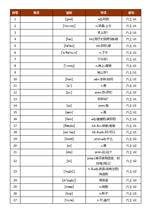
中文 adj.好的 n.早晨;上午 早上好! int.(用于打招呼)嗨;喂 int.你好;喂 n.下午 下午好! n.晚上;黄昏 晚上好! adv.怎样;如何
v.是 pron.你;你们
你好吗? pron.我
v.是 adj.健康的;美好的 int.&n.感谢;谢谢 int.&adv.好;可以
pron.adj.什么 v.是
pron.这;这个 prep.(表示使用语言、材
料等)用;以 n.&adj.英语;英格兰的;
英语的 用英语 n.地图 n.杯子 n 尺;直尺
单元 六上 U1 六上 U1 六上 U1 六上 U1 六上 U1 六上 U1 六上 U1 六上 U1 六上 U1 六上 U1 六上 U1 六上 U1 六上 U1 六上 U1 六上 U1 六上 U1 六上 U1 六上 U1 六上 U2 六上 U2 六上 U2
n.名字;名称
六上 U4
54
[naɪs]
adj.令人愉快的;宜人的 六上 U4
常用于原形动词之前,
UG416S6446JSH-PL中文资料

DQM3
DQ24 DQ25 DQ26
DQ12 DQ13 DQ14 DQ15
DQ44 DQ45 DQ46 DQ47
VSS
DQ56
Gold
Hale Waihona Puke DQ57DQ58 DQ59
VSS
NC NC CLK0
56 58 60 62 64 66 68 70 72
VSS
NC NC CKE0
127 129 131 133 135 137 139 141 143
30 32 34
101 103 105
VCC A6
A8
102 106
VCC A7
BA0
VSS
36
VSS
107
VSS
A9
VSS
BA1
DQ8 DQ9
38 40 42 44 48 50 52 54
DQ40 DQ41 DQ42 DQ43
109 111
A10
A11 VCC
DQM6 DQM7
ORDERING INFORMATION
DQM0 DQM1
24 26
DQM4 DQM5
95 97
DQ21 DQ22
U N IG EN
-0.3 to + 4.6V 0 to + 70°C -55°C to + 125°C 50mA 8W
VCC
A0 A1 A2
28
VCC
A3 A4 A5
99
DQ23
100 104 108 110 112 114 116 118 120 122 124 126 128 130
65 67 69 71
VSS
SDA
VSS
UG416S6448JSG-PH中文资料

A0 ~ An, BA0 & 1 RAS
SDRAM U0 ~ U7 SDRAM U0 ~ U7 SDRAM U0 ~ U7 SDRAM U0 ~ U7 SDRAM U0 ~ U7
U6
CAS WE
DQM7
DQ56 DQ57 DQ58 DQ59 DQ60 DQ61 DQ62 DQ63
DQM DQ0 DQ1 DQ2 DQ3 DQ4 DQ5 DQ6 DQ7
based on 8 pcs 16M x 8 SDRAM with LVTTL, 4 banks & 4K Refresh
The UG416S6448JSG-PL/PH is a 16Mbits x 64 Sync DRAM module. The UG416S6448JSG-PL/PH is assembled using 8 pcs of 16M x 8 with 4 Banks Sync DRAMs in 54 pin TSOP packages mounted on 144 pin unbuffered printed circuit board.
DQM0 DQM1
24 26
DQM4 DQM5
95 97
DQ21 DQ22
96 98
U N IG EN
-0.3 to + 4.6V 0 to + 70°C -55°C to + 125°C 50mA 8W
VCC
A0 A1 A2
28
VCC
A3 A4 A5
99
Hale Waihona Puke DQ2310030 32 34
101 103 105
VCC A6
A8
102
VCC A7
加法运算电路
中文摘要加法运算电路时一种通过数字运算实现加法的运算。
为了更好的实现加法器的功能,本次试验实现的是俩位十进制数相加,最多能实现15加15的加法电路。
由五部分组成键盘及编码电路、加数寄存器A和被加数寄存器B、加法运算电路、4bit二进制码加法的BCD 调整通过按键控制。
主要组成部分有数字输入与控制寄存电路74LS系列利用两块74LS194寄存器并行输入两个数据A3A2A1A0、B3B2B1B074LS283加法器中进行加法运算。
进行bcd码调整,最后显示结果。
由两异或门两与门和一或门组成全加器,可实现一位二进制加逻辑运算,四位二进制数并行相加的逻辑运算可采用四个全加器串行进位的方式来实现,将低位的进位输出信号接到高位的进位输入端,四个全加器依次串行连接,并将最低位的进位输入端接逻辑“0”,就组成了一个可实现四位二进制数并行相加的逻辑电路。
关键词加法运算电路,寄存器,加法器,二进制目录课程设计任务书.................................................................................................................错误!未定义书签。
中文摘要 (I)1 设计任务描述 (1)1.1设计题目:加法运算电路: (1)1.2 设计要求 (1)1.2.1 设计目的 (1)1.2.2 基本要求 (1)1.2.3 发挥部分 (1)2设计思路 (2)3设计方框图 (3)4各部分电路设计及参数计算 (4)4.1键盘设计电路 (4)4.2寄存器电路 (5)4.2.1寄存器74LS194N电路设计及工作原理 (5)4.3加法器工作原理 (6)4.4译码显示电路 (7)4.4.1 译码显示电路的连接 (7)4.4.2 译码显示电路的工作原理 (7)5工作过程分析 (8)5.1加法工作过程 (8)6元器件清单 (12)7主要元器件介绍 (13)7.110-4线BCD优先编码器74147 (13)7.1.1引脚图 (13)7.1.2功能表 (13)7.1.3 功能介绍 (14)7.2 寄存器74LS194N (14)7.2.1引脚图 (14)7.2.2 功能表 (14)7.3.3 功能介绍 (15)7.4 加法器74S283N (15)7.4.1 引脚图 (15)7.4.2 功能表 (16)7.4.3 功能介绍 (16)小结 (17)致谢 (18)参考文献 (19)附录 A1 逻辑电路图 (20)1 设计任务描述1.1设计题目:加法运算电路:1.2设计要求1.2.1 设计目的(1)掌握1位十进制数加法运算电路的构成、原理与设计方法;(2)熟悉集成电路的使用方法。
EL4441CN资料

EL4421C 22C 41C 42C 43C 44CJanuary1996RevC Note All information contained in this data sheet has been carefully checked and is believed to be accurate as of the date of publication however this data sheet cannot be a‘‘controlled document’’ Current revisions if any to these specifications are maintained at the factory and are available upon your request We recommend checking the revision level before finalization of your design documentation1994Elantec IncFeaturesUnity or a2-gain bandwidth of80MHz70dB off-channel isolation at4MHzDirectly drives high-impedanceor75X loads02%and 02 differential gainand phase errors8ns switching timek100mV switching glitch0 2%loaded gain errorCompatible with g3V to g15Vsupplies160mW maximum dissipation atg5V suppliesOrdering InformationPart No Temp Range Package OutlineEL4421CN b40 C to a85 C8-Pin PDIP MDP0031EL4421CS b40 C to a85 C8-Pin SO MDP0027EL4422CN b40 C to a85 C8-Pin PDIP MDP0031EL4422CS b40 C to a85 C8-Pin SO MDP0027EL4441CN b40 C to a85 C14-Pin PDIP MDP0031EL4441CS b40 C to a85 C14-Pin SO MDP0027EL4442CN b40 C to a85 C14-Pin PDIP MDP0031EL4442CS b40 C to a85 C14-Pin SO MDP0027EL4443CN b40 C to a85 C14-Pin PDIP MDP0031EL4443CS b40 C to a85 C14-Pin SO MDP0027EL4444CN b40 C to a85 C14-Pin PDIP MDP0031EL4444CS b40 C to a85 C14-Pin SO MDP0027General DescriptionThe EL44XX family of video multiplexed-amplifiers offers avery quick8ns switching time and low glitch along with verylow video distortion The amplifiers have good gain accuracyeven when driving low-impedance loads To save power the am-plifiers do not require heavy loading to remain stableThe EL4421and EL4422are two-input multiplexed amplifiersThe-inputs of the input stages are wired together and the de-vice can be used as a pin-compatible upgrade from theMAX453The EL4441and EL4442have four inputs also with commonfeedback These may be used as upgrades of the MAX454The EL4443and EL4444are also4-input multiplexed amplifi-ers but both positive and negative inputs are wired separatelyA wide variety of gain-and phase-switching circuits can be builtusing independent feedback paths for each channelThe EL4421 EL4441 and EL4443are internally compensatedfor unity-gain operation The EL4422 EL4442 and EL4444arecompensated for gains of a2or more especially useful for driv-ing back-matched cablesThe amplifiers have an operational temperature of b40 C toa85 C and are packaged in plastic8-and14-pin DIP and8-and14-pin SOThe EL44XX multiplexed-amplifier family is fabricated withElantec’s proprietary complementary bipolar process whichgives excellent signal symmetry and is very ruggedConnection DiagramsEL4421 EL44224421–1EL4441 EL44424421–2EL4443 EL44444421–3 Manufactured under U S Patent No 5 352 9872T D i s 3 3 i n34T D i s 2 4 i nTypical Performance Curves ContdV S e g 5V A V e a 1Frequency Response for Various Loads EL4421 EL4441 and EL44434421–9V S e g 5V A V e a 2Frequency Response for Various Loads EL4422 EL4442 and EL44444421–10V S e g 15V A V e a 1for Various LoadsFrequency Response 4421–11V S e g 15V A V e a 2Frequency Response for Various Loads EL4422 EL4442 and EL44444421–12Phase vs Frequency EL4443Open-Loop Gain and 4421–13Phase vs FrequencyEL4444Open-Loop Gain and 4421–375Typical Performance Curves Contdand Peaking vs Supply Voltageb3dB Bandwidth SlewrateEL4421 EL4441 and EL44434421–14and Peaking vs Supply Voltageb3dB Bandwidth SlewrateEL4422 EL4442 and EL44444421–15 vs Temperature A V e a1 R L e500XBandwidth Slewrate and PeakingEL4421 EL4441 and EL44434421–16A V e a2 R L e150X R I e R G e270X C F e3pFSlewrate and Peaking vs TemperatureEL4422 EL4442 and EL4444Bandwidth4421–17 vs Load Resistanceb3dB Bandwidth and Gain ErrorEL4421 EL4441 and EL44434421–18Input Noise vs Frequency4421–196Typical Performance Curves ContdA V e a1 R L e500X F e3 58MHzand Phase Errors vs Input OffsetEL4421 EL4441 and EL4443Differential Gain4421–20A V e a2 R L e150X F e3 58MHzand Phase Error vs Input OffsetEL4422 EL4442 and EL4444Differential Gain4421–21A V e a1 F e3 58MHz V OFFSET e0x0 714Vand Phase Error vs Load ResistanceEL4421 EL4441 and EL4443Differential Gain4421–22vs Load ResistanceEL4443and EL4444Open-Loop Gain4421–23 with Supply VoltageChange in V OS A V and I B4421–24and A V vs TemperatureChange in V OS I B4421–257Typical Performance Curves Contdto Uncorrelated Sinewave and BackSwitching from Grounded Input Switching Waveforms4421–26Switching GlitchChannel-to-Channel 4421–27Feedthrough vs Frequency Unselected ChannelEL4421 EL4441 and EL44434421–28Feedthrough vs FrequencyUnselected ChannelEL4422 EL4442 and EL44444421–29Input and Output Range vsEL4443and EL4444Supply Voltage (Output Unloaded)4421–308Typical Performance Curves ContdSupply VoltageSupply Current vs 4421–31TemperatureSupply Current vs 4421–32Ambient TemperaturePower Dissipation vs 8-Pin Package4421–33Ambient TemperaturePower Dissipation vs 14-Pin Package4421–34Applications Information General DescriptionThe EL44XX family of video mux-amps are com-posed of two or four input stages whose inputs are selected and control an output stage One of the inputs is active at a time and the circuit be-haves as a traditional voltage-feedback op-amp for that input rejecting signals present at the un-selected inputs Selection is controlled by one or two logic inputsThe EL4421 EL4422 EL4441 and EL4442have all b inputs wired in parallel allowing a single feedback network to set the gain of all inputs These devices are wired for positive gains TheEL4443and EL4444 on the other hand have all a inputs and b inputs brought out separately so that the input stage can be wired for independent gains and gain polarities with separate feedback networksThe EL4421 EL4441 and EL4443are compen-sated for unity-gain stability while the EL4422 EL4442 and EL4444are compensated for a fed-back gain of a 2 ideal for driving back-terminat-ed cables or maintaining bandwidth at higher fed-back gains9Applications Information Contd Switching CharacteristicsThe logic inputs work with standard TTL levels of 0 8V or less for a logic 0and 2 0V or more for a logic 1 making them compatible for TTL andCMOS drivers The ground pin is the logic threshold biasing reference The simplified input circuitry is shown below4421–35Figure 1 Simplified Logic Input CircuitryThe ground pin draws a maximum DC current of 6m A and may be biased anywhere between (V b )a 2 5V and (V a )b 3 5V The logic inputs may range from (V b )a 2 5V to V a and are ad-ditionally required to be no more negative thanV(Gnd pin)b 4V and no more positive than V(Gnd pin)a 6VFor example within these constraints we can power the EL44XX’s from a 5V and a 12V with-out a negative supply by using these connections4421–36Figure 2 Using the EL44XX Mux Amps with a 5V and a 12V Supplies10Applications Information ContdThe logic input(s)and ground pin are shifted 2 5V above system ground to correctly bias the mux-amp Of course all the signal inputs and output will have to be shifted2 5V above system ground to ensure proper signal path biasingA final caution the ground pin is also connected to the IC’s substrate and frequency compensation components The ground pin must be returned to system ground by a short wire or nearby bypass capacitor In figure2 the22K X resistors also serve to isolate the bypassed ground pin from the a5V supply noiseSignal AmplitudesSignal input and output voltages must be be-tween(V b)a2 5V and(V a)b2 5V to ensure linearity Additionally the differential voltage on any input stage must be limited to g6V to pre-vent damage In unity-gain connections any in-put could have g3V applied and the output would be at g3V putting us at our6V differen-tial limit Higher-gain circuit applications divide the output voltage and allow for larger outputs For instance at a gain of a2the maximum inputis again g3V and the output swing is g6V The EL4443or EL4444can be wired for inverting gain with even more amplitude possibleThe output and positive inputs respond to over-loading amplitudes correctly that is they simply clamp and remain monotonic with increasinga input overdrive A condition exists howeverwhere the b input of an active stage is overdriven by large outputs This occurs mainly in unity-gain connections and only happens for negative inputs The overloaded input cannot control the feedback loop correctly and the output can be-come non-monotonic A typical scenario has the circuit running on g5V supplies connected for unity gain and the input is the maximum g3V Negative input extremes can cause the output to jump from b3V to around b2 3V This will nev-er happen if the input is restricted to g2 5V which is the guaranteed maximum input compli-ance with g5V supplies and is not a problem with greater supply voltages Connecting the feedback network with a divider will prevent the overloaded output voltage from being large enough to overload the b input and monotonic 11Applications Information Contdbehavior is assured In any event keeping signals within guaranteed compliance limits will assure freedom from overload problemsThe input and output ranges are substantially constant with temperaturePower SuppliesThe mux-amps work well on any supplies from g3V to g15V The supplies may be of different voltages as long as the requirements of the Gnd pin are observed(see the Switching Characteris-tics section for a discussion) The supplies should be bypassed close to the device with short leads 4 7m F tantalum capacitors are very good and no smaller bypasses need be placed in parallel Ca-pacitors as small as0 01m F can be used if small load currents flowSingle-polarity supplies such as a12V with a5V can be used as described in the Switching Characteristics section The inputs and outputs will have to have their levels shifted above ground to accommodate the lack of negative sup-plyThe dissipation of the mux-amps increases with power supply voltage and this must be compati-ble with the package chosen This is a close esti-mate for the dissipation of a circuitP D e2V S c I s max a(V S–V O)c V O R PARWhere I s max is the maximum supply cur-rentV S is the g supply voltage(as-sumed equal)V O if the output voltageR PAR is the parallel of all resistorsloading the outputFor instance the EL4422draws a maximum of 14mA and we might require a2V peak output into150X and a270X a270X feedback divider The R PAR is117X The dissipation with g5V supplies is191mW The maximum Supply volt-age that the device can run on for a given P D and the other parameter isV S max e(P D a V O2 R PAR) 2Is a V O R PAR)The maximum dissipation a package support isP D max e(T D max-T A max) R THWhere T D max is the maximum die temper-ature 150 C for reliability less to re-tain optimum electrical performanceT A max is the ambient temperature70 for commercial and85 C for indus-trial rangeR TH is the thermal resistance of themounted package obtained from datasheet dissipation curvesThe most difficult case is the SO-8package Witha maximum die temperature of150 C and a maxi-mum ambient temperature of85 the65 temper-ature rise and package thermal resistance of 170 W gives a maximum dissipation of382mW This allows a maximum supply voltage of g9 2V for the EL4422operated in our example If the EL4421were driving a light load(R PAR x%) it could operate on g15V supplies at a70 maxi-mum ambientThe EL4441through EL4444can operate on g12V supplies in the SO package and all parts can be powered by g15V supplies in DIP pack-agesOutput LoadingThe output stage of the mux-amp is very power-ful and can source80mA and sink120mA Of course this is too much current to sustain and the part will eventually be destroyed by excessive dissipation or by metal traces on the die opening The metal traces are completely reliable while de-livering the30mA continuous output given in the Absolute Maximum Ratings table in this data sheet or higher purely transient currents Gain or gain accuracy degrades only10%from no load to100X load Heavy resistive loading will degrade frequency response and video distortion only a bit becoming noticeably worse for loads k100X12Applications Information ContdCapacitive loads will cause peaking in the fre-quency response If capacitive loads must be driv-en a small-valued series resistor can be used to isolate it 12X to51X should suffice A22X series resistor will limit peaking to2 5dB with even a 220pF loadInput ConnectionsThe input transistors can be driven from resistive and capacitive sources but are capable of oscilla-tion when presented with an inductive input It takes about80nH of series inductance to make the inputs actually oscillate equivalent to four inches of unshielded wiring or about6 of unter-minated input transmission line The oscillation has a characteristic frequency of500MHzOften simply placing one’s finger(via a metal probe)or an oscilloscope probe on the input will kill the oscillation Normal high-frequency con-struction obviates any such problems where the input source is reasonably close to the mux-amp input If this is not possible one can insert series resistors of around51X to de-Q the inputsFeedback ConnectionsA feedback divider is used to increase circuit gain and some precautions should be observed The first is that parasitic capacitance at the b in-put will add phase lag to the feedback path and increase frequency response peaking or even cause oscillation One solution is to choose feed-back resistors whose parallel value is low The pole frequency of the feedback network should be maintained above at least200MHz For a3pF parasitic this requires that the feedback divider have less than265X impedance equivalent to two510X resistors when a gain of a2is desired Alternatively a small capacitor across R F can be used to create more of a frequency-compensated divider The value of the capacitor should match the parasitic capacitance at the b input It is also practical to place small capacitors across both the feedback resistors(whose values maintain the de-sired gain)to swamp out parasitics For instance two10pF capacitors across equal divider resis-tors will dominate parasitic effects and allow a higher divider resistanceThe other major concern about the divider con-cerns unselected-channel crosstalk The differen-tial input impedance of each input stage isaround200K X The unselected input’s signalsources thus drive current through that input im-pedance into the feedback divider inducing anunwanted output The gain from unselected in-put to output the crosstalk attenuation if R FR IN In unity-gain connection the feedback resis-tor is0X and very little crosstalk is induced Fora gain of a2 the crosstalk is about b60dBFeedthrough AttenuationThe channels have different crosstalk levels withdifferent inputs Here is the typical attenuationfor all combinations of inputs for the mux-ampsat3 58MHzFeedthrough of EL4441and EL4443at3 58MHzIn1In2In3In4InputsSelectA1A000Selected b77dB b90dB b92dB01b80dB Selected b77dB b90dB10b101dB b76dB Selected b66dB11b96dB b84dB b66dB SelectedFeedthrough of EL4421at3 58MHzIn1In2Channel Select0Selected b88dBInput A01b93dB SelectedSwitching GlitchesThe output of the mux-amps produces a small‘‘glitch’’voltage in response to a logic inputchange A peak amplitude of only about90mVoccurs and the transient settles out in20ns Theglitch does not change amplitude with differentgain settingsWith the four-input multiplexers when two logicinputs are simultaneously changed the glitchamplitude doubles The increase can be a avoidedby keeping transitions at least6ns apart Thiscan be accomplished by inserting one gate delayin one of the two logic inputs when they are trulysynchronous13TDis5inTDis5in元器件交易网KNALB14KNALB15E L 4421C 22C 41C 42C J a n u a r y 1996R e v CGeneral DisclaimerSpecifications contained in this data sheet are in effect as of the publication date shown Elantec Inc reserves the right to make changes in the circuitry or specifications contained herein at any time without notice Elantec Inc assumes no responsibility for the use of any circuits described herein and makes no representations that they are free from patent infringementElantec Inc 1996Tarob Court Milpitas CA 95035Telephone (408)945-1323(800)333-6314Fax (408)945-9305European Office 44-71-482-4596WARNING Life Support PolicyElantec Inc products are not authorized for and should not be used within Life Support Systems without the specific written consent of Elantec Inc Life Support systems are equipment in-tended to support or sustain life and whose failure to perform when properly used in accordance with instructions provided can be reasonably expected to result in significant personal injury or death Users contemplating application of Elantec Inc products in Life Support Systems are requested to contact Elantec Inc factory headquarters to establish suitable terms conditions for these applications Elantec Inc ’s warranty is limited to replace-ment of defective components and does not cover injury to per-sons or property or other consequential damagesPrinted in U S A16。
DG444中文资料

7
D4
Drain (Output) Terminal for Switch 4
8
IN4
Logic Control for Switch 4
9
IN3
Logic Control for Switch 3
10
D3
Drain (Output) Terminal for Switch 3
11
S3
Source (Input) Terminal for Switch 3
Applications
• Audio Switching • Battery Operated Systems • Data Acquisition • Hi-Rel Systems • Sample and Hold Circuits • Communication Systems • Automatic Test Equipment
2
D1
Drain (Output) Terminal for Switch 1
3
S1
Source (Input) Terminal for Switch 1
4
V-
Negative Power Supply Terminal
5
GND Ground Terminal (Logic Common)
6
S4
Source (Input) Terminal for Switch 4
115
Maximum Junction Temperature (Plastic Packages) . . . . . . . 150oC
Maximum Storage Temperature Range . . . . . . . . . . -65oC to 150oC
1N4744A-A中文资料

1N4728A - 1N4761A1.0W ZENEDIODENote: 1. Valid provided that leads are kept at T L @ 50°C with lead length = 9.5mm (3/8”) from case.2. EC Directive 2002/95/EC (RoHS) revision 13.2.2003. Glass and High Temperature Solder Exemptions Applied where applicable,see EU Directive Annex Notes 5 and 7.Mechanical Data·1.0 Watt Power Dissipation · 3.3V - 75V Nominal Zener Voltage ·Standard V Z Tolerance is 5%·Lead Free Finish, RoHS Compliant (Note 2)·Case: DO-41·Case Material: Glass. UL Flammability Classification Rating 94V-0·Moisture Sensitivity: Level 1 per J-STD-020C ·Terminals: Finish ¾ Sn96.5Ag3.5. Solderable per MIL-STD-202, Method 208·Polarity: Cathode Band ·Marking: Type Number·Weight: 0.35 grams (approximate)FeaturesElectrical Characteristics @ T A = 25°C unless otherwise specifiedNotes: 3. Measured under thermal equilibrium and dc (I ZT) test conditions.4. The Zener impedance is derived from the 60 Hz ac voltage which results when an ac current having an rms value equal to10% of the Zener current (I ZT or I ZK) is superimposed on I ZT or I ZK. Zener impedance is measured at two points to insure asharp knee on the breakdown curve and to eliminate unstable units.Notes: 5. *Add "-A" or "-T" to the appropriate type number in Table 1. Example: 6.2V Zener = 1N4735A-A for ammo pack. 6. For packaging details, visit our website at /datasheets/ap02008.pdf00.20.40.60.81.004080120160200P , T O T A L P O W E R D I S S I P A T I O N (W )d T , AMBIENT TEMPERATURE ( C)A Fig.1 Power Dissipation vs Ambient Temperature0250515202530l, Lead Length (mm)Fig. 2 Typical Thermal Resistance vs. Lead Length10200501001501101001000110100V , ZENER VOLTAGE (V)Z Fig. 4 Typical Zener Impedance vs. Zener Voltage1101001000102030405060C ,D I O DE C A P A C I T A N C E (pF )j V , ZENER VOLTAGE (V)Z Fig.3, Junction Capacitance vs Zener Voltagef = 1MHz T = 25CA V = 0V R V = 2V R V = 5V R V = 20VR V = 30VR Ordering Information(Note 6)IMPORTANT NOTICEDiodes Incorporated and its subsidiaries reserve the right to make modifications, enhancements, improvements, corrections or other changes without further notice to any product herein. Diodes Incorporated does not assume any liability arising out of the application or use of any product described herein; neither does it convey any license under its patent rights, nor the rights of others. The user of products in such applications shall assume all risks of such use and will agree to hold Diodes Incorporated and all the companies whose products are represented on our website, harmless against all damages.LIFE SUPPORTDiodes Incorporated products are not authorized for use as critical components in life support devices or systems without the expressed written approval of the President of Diodes Incorporated.。
三种车型VIN含义及常见车型代码
常见车型VIN含义及车型代码前言VIN(Vehicle Identification Number),中文名叫车辆识别代码, 是制造厂为了识别而给一辆车指定的一组字码。
SAE标准规定:VIN码由17位字符组成,所以俗称十七位码。
它包含了车辆的生产厂家、年代、车型、车身型式及代码、发动机代码及组装地点等信息。
正确解读VIN码,对于我们正确地识别车型,以致进行正确地诊断和维修都是十分重要的。
车辆识别代码经过排列组合,可以使同一车型的车在30年之内不会发生重号现象,具有对车辆的唯一识别性,因此可称为"汽车身份证"。
VIN的历史可以追溯到1949年。
但直到1981年之前,标准一直处于变换中。
比如:1965-1969年的VIN有9位,当生产量超过1百万之后采用10位;1970-1980年的VIN则固定为10位。
现行的17位汽车识别码始于1981年。
我国已于1996年底颁布了相关标准,并已于1997年开始实行。
实际操作中,1999年1月1日以后被初次登记的车辆必须拥有车辆识别代码。
VIN中不会包含 I、O、Q 三个英文字母。
从左到右数起,第十位编码为车辆出厂年月。
目录一、奔驰类1.1奔驰车型VIN含义:1.2奔驰车型VIN所在位置:1.3常见年份对照表:1.4奔驰车型常见发动机代码1.5奔驰变速箱型号含义:二、宝马类2.1宝马车型VIN含义:2.2宝马车型常见车型代码:2.3宝马车型VIN所在位置:2.4宝马变速箱型号含义:三、奥迪类3.1奥迪车型VIN含义:3.2奥迪车型常见车型代码:3.3奥迪车型VIN所在位置:3.4奥迪变速箱型号含义:1.1奔驰VIN含义WDB 220 167 1A326964WDB表示德国生产常用见生产地名代表WDB-West germany Daimler-Benz 德国WDC---M-Class Europe 欧洲产M-ClassWEB---EVOBUS Mercedes-Benz 奔驰-EVOBUSWKK---EVOBUS Setra Setra产的EVOBUS3AM---Mexico 墨西哥4JG----M-Class except Europe 欧洲外产M-Class8AB-Argentine 阿根廷8AC-Argentine 阿根廷9BM-Brazil 巴西ADB-South Africa 南非KPA---South Korea Transporter 韩国KPD--- South Korea 韩国KPG--- South Korea 韩国NMB---Turkey 土耳其V AG---G-Wagon Steyr Steyr产的G-ClassVF9---EVOBUS France 法国-EVOBUSVSA---Spain 西班牙LE4---China 中国WDB 220 167 1A326964220表示S-Class常用见级别所代表车型底盘号内部分组100-299 轿车;300-399卡车/公共汽车;400-499 专用车;600-699 卡车;700-799 主要部件WDB 220 167 1A3269640—Sedan1—LWB Sedan 加长2—Station Wagen 旅行车3---Coupe 双门运动型轿车4---Cabriolet/roadster 双门敞篷跑车5---Chassis with partial body 轿车底盘6--LWB Chassis with partial body加长轿车底盘7—Sports8—Pull manWDB 220 167 1A32696400-09 四缸柴油发动机04=E22010-19 五缸柴油发动机10=E25020-29 六缸柴油发动机20=E30030-49四缸汽油发动机35=E20050-69 六缸汽油发动机55=E320 63=S320 67=S35070-79 八---十二缸汽油发动机75=S60080-84 AWD 替代能源发动机85-99 Alternative propulsion替代能源动力WDB 220 167 1A3269641=左舵2=右舵WDB 220 167 1A326964A,B,C,D,E=Sindelfingen(新德芬根)F,G,H=Breman(布莱门)J=RastattWDB 220 167 1A326964326964装配出厂顺序号1. 2奔驰车架号VIN的位置1、行驶证2、前挡风玻璃左前下部3、诊断电脑、数据卡4、前乘客座椅底下,右后座椅下。