L7852CD2T-TR中文资料
79xx系列
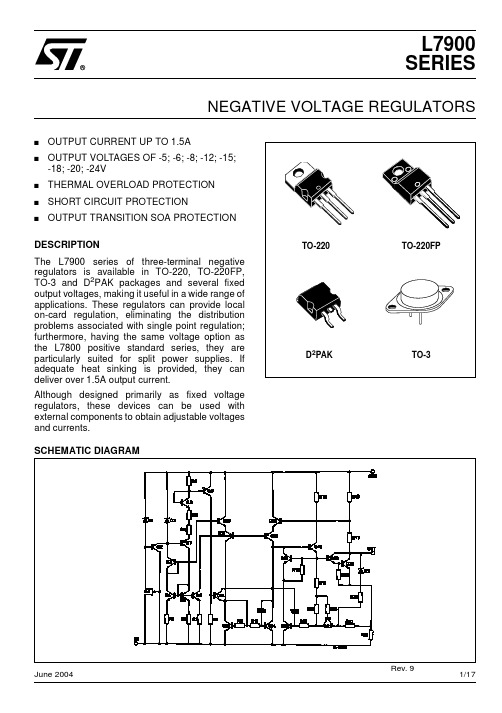
D2PAK
TO-3
June 2004
Rev. 9
1/17
L7900 SERIES
L7815CD2T中文资料

L7800SERIESPOSITIVE VOLTAGE REGULATORSJanuary 1997s OUTPUT CURRENT UP TO 1.5AsOUTPUT VOLTAGES OF 5;5.2;6;8;8.5;9;12;15;18;24Vs THERMAL OVERLOAD PROTECTION s SHORT CIRCUIT PROTECTIONsOUTPUT TRANSITION SOA PROTECTIONDESCRIPTIONThe L7800series of three-terminal positive regulators is available in TO-220ISOWATT220TO-3and D 2PAK packages and several fixed output voltages,making it useful in a wide range of applications.These regulators can provide local on-card regulation,eliminating the distribution problems associated with single point regulation.Each type employs internal current limiting,thermal shut-down and safe area protection,making it essentially indestructible.If adequate heat sinking is provided,they can deliver over 1A output current.Although designed primarily as fixed voltage regulators,these devices can be used with external components to obtain adjustable voltages and currents.12TO-3123TO-220ISOWATT22012313D 2PAKBLOCK DIAGRAM1/25CONNECTION DIAGRAM AND ORDERING NUMBERS (top view)TO-220&ISOWATT220TO-3D 2PAKTHERMAL DATASymbolParameterD 2PAK TO-220ISOWATT220TO-3UnitR t hj-case R th j-a mb Thermal Resistance Junction-case Max Thermal Resistance Junction-ambient Max 362.5350460435o C/W oC/WType TO-220D 2PAK (*)ISOWATT220TO-3Output VoltageL7805L7805C L7852C L7806L7806C L7808L7808C L7885C L7809C L7812L7812C L7815L7815C L7818L7818C L7820L7820C L7824L7824CL7805CV L7852CV L7806CV L7808CV L7885CV L7809CV L7812CV L7815CV L7818CV L7820CV L7824CVL7805CD2T L7852CD2T L7806CD2T L7808CD2T L7885CD2T L7809CD2T L7812CD2T L7815CD2T L7818CD2T L7820CD2T L7824CD2TL7805CP L7852CP L7806CP L7808CP L7885CP L7809CP L7812CP L7815CP L7818CP L7820CP L7824CPL7805T L7805CT L7852CT L7806T L7806CT L7808T L7808CT L7885CT L7809CT L7812T L7812CT L7815T L7815CT L7818T L7818CT L7820T L7820CT L7824T L7824CT5V 5V 5.2V 6V 6V 8V 8V 8.5V 9V 12V 12V 15V 15V 18V 18V 20V 20V 24V 24V(*)AVAILABLE IN TAPE AND REEL WITH ”-TR”SUFFIXABSOLUTE MAXIMUM RATINGSSymbol ParameterValue Unit V i DC Input Voltage (for V O =5to 18V)(for V O =20,24V)3540V VI o Output Current Internally limited P t ot Power DissipationInternally limited T o p Operating Junction Temperature Range (for L7800)(for L7800C )-55to 1250to 150o C o C T stgStorage Temperature Range-40to 150oCL78002/25L7800 APPLICATION CIRCUITSCHEMATIC DIAGRAM3/25TEST CIRCUITSFigure3:Ripple Rejection.Figure2:Load Regulation.Figure1:DC Parameter L78004/25ELECTRICAL CHARACTERISTICS FOR L7806(refer to the test circuits,T j =-55to 150o C,V i =15V,I o =500mA,C i =0.33µF,C o =0.1µF unless otherwise specified)Symbol ParameterTest Conditions Min.Typ.Max.Unit V o Output Voltage T j =25oC 5.756 6.25V V o Output Voltage I o =5mA to 1A P o ≤15WV i =9to 21V 5.6566.35V ∆V o *Line Regulation V i =8to 25V T j =25oCV i =9to 13VT j =25oC6030mV mV ∆V o *Load Regulation I o =5to 1500mA T j =25o CI o =250to 750mA T j =25oC10030mV mV I d Quiescent Current T j =25o C 6mA ∆I d Quiescent Current Change I o =5to 1000mA 0.5mA ∆I d Quiescent Current Change V i =9to 25V 0.8mA ∆V o ∆T Output Voltage Drift I o =5mA0.7mV/oCeN Output Noise Voltage B =10Hz to 100KHz T j =25oC 40µV/V O SVR Supply Voltage Rejection V i =9to 19V f =120Hz65dB V d Dropout Voltage I o =1A T j =25o C2 2.5V R o Output Resistance f =1KHz 19m ΩI sc Short Circuit Current V i =35V T j =25oC0.75 1.2A I s cpShort Circuit Peak CurrentT j =25o C1.32.23.3AELECTRICAL CHARACTERISTICS FOR L7805(refer to the test circuits,T j =-55to 150o C,V i =10V,I o =500mA,C i =0.33µF,C o =0.1µF unless otherwise specified)Symbol ParameterTest Conditions Min.Typ.Max.Unit V o Output Voltage T j =25oC 4.85 5.2V V o Output Voltage I o =5mA to 1A P o ≤15WV i =8to 20V 4.655 5.35V ∆V o *Line Regulation V i =7to 25V T j =25o CV i =8to 12VT j =25oC315025mV mV ∆V o *Load Regulation I o =5to 1500mA T j =25oCI o =250to 750mA T j =25oC10025mV mV I d Quiescent Current T j =25o C 6mA ∆I d Quiescent Current Change I o =5to 1000mA 0.5mA ∆I d Quiescent Current Change V i =8to 25V 0.8mA ∆V o ∆T Output Voltage Drift I o =5mA0.6mV/oCeN Output Noise Voltage B =10Hz to 100KHz T j =25o C 40µV/V O SVR Supply Voltage Rejection V i =8to 18V f =120Hz68dB V d Dropout Voltage I o =1A T j =25oC 2 2.5V R o Output Resistance f =1KHz 17m ΩI sc Short Circuit Current V i =35V T j =25oC0.75 1.2A I s cpShort Circuit Peak CurrentT j =25oC1.32.23.3A*Load and line regulation are specified at constant junction temperature.Changes in V o due to heating effects must be taken into account separately.Pulce testing with low duty cycle is used.L78005/25ELECTRICAL CHARACTERISTICS FOR L7812(refer to the test circuits,T j =-55to 150o C,V i =19V,I o =500mA,C i =0.33µF,C o =0.1µF unless otherwise specified)Symbol ParameterTest Conditions Min.Typ.Max.Unit V o Output Voltage T j =25oC11.51212.5V V o Output Voltage I o =5mA to 1A P o ≤15W V i =15.5to 27V11.41212.6V ∆V o *Line Regulation V i =14.5to 30V T j =25oCV i =16to 22V T j =25oC 12060mV mV ∆V o *Load Regulation I o =5to 1500mA T j =25o CI o =250to 750mA T j =25oC10060mV mV I d Quiescent Current T j =25o C 6mA ∆I d Quiescent Current Change I o =5to 1000mA 0.5mA ∆I d Quiescent Current Change V i =15to 30V 0.8mA ∆V o ∆T Output Voltage Drift I o =5mA1.5mV/oCeN Output Noise Voltage B =10Hz to 100KHz T j =25o C 40µV/V O SVR Supply Voltage Rejection V i =15to 25V f =120Hz61dB V d Dropout Voltage I o =1A T j =25o C2 2.5V R o Output Resistance f =1KHz 18m ΩI sc Short Circuit Current V i =35V T j =25oC0.75 1.2A I s cpShort Circuit Peak CurrentT j =25o C1.32.23.3AELECTRICAL CHARACTERISTICS FOR L7808(refer to the test circuits,T j =-55to 150o C,V i =14V,I o =500mA,C i =0.33µF,C o =0.1µF unless otherwise specified)Symbol ParameterTest Conditions Min.Typ.Max.Unit V o Output Voltage T j =25oC7.788.3V V o Output Voltage I o =5mA to 1A P o ≤15W V i =11.5to 23V7.688.4V ∆V o *Line Regulation V i =10.5to 25V T j =25o CV i =11to 17V T j =25oC 8040mV mV ∆V o *Load Regulation I o =5to 1500mA T j =25oCI o =250to 750mA T j =25oC10040mV mV I d Quiescent Current T j =25o C 6mA ∆I d Quiescent Current Change I o =5to 1000mA 0.5mA ∆I d Quiescent Current Change V i =11.5to 25V 0.8mA ∆V o ∆T Output Voltage Drift I o =5mA1mV/oCeN Output Noise Voltage B =10Hz to 100KHz T j =25o C 40µV/V O SVR Supply Voltage Rejection V i =11.5to 21.5V f =120Hz62dB V d Dropout Voltage I o =1A T j =25oC 2 2.5V R o Output Resistance f =1KHz 16m ΩI sc Short Circuit Current V i =35V T j =25oC0.75 1.2A I s cpShort Circuit Peak CurrentT j =25oC1.32.23.3A*Load and line regulation are specified at constant junction temperature.Changes in V o due to heating effects must be taken into account separately.Pulce testing with low duty cycle is used.L78006/25ELECTRICAL CHARACTERISTICS FOR L7818(refer to the test circuits,T j =-55to 150o C,V i =26V,I o =500mA,C i =0.33µF,C o =0.1µF unless otherwise specified)Symbol ParameterTest Conditions Min.Typ.Max.Unit V o Output Voltage T j =25oC 17.31818.7V V o Output Voltage I o =5mA to 1A P o ≤15W V i =22to 33V 17.11818.9V ∆V o *Line Regulation V i =21to 33V T j =25oCV i =24to 30VT j =25oC18090mV mV ∆V o *Load Regulation I o =5to 1500mA T j =25o CI o =250to 750mA T j =25oC18090mV mV I d Quiescent Current T j =25o C 6mA ∆I d Quiescent Current Change I o =5to 1000mA 0.5mA ∆I d Quiescent Current Change V i =22to 33V 0.8mA ∆V o ∆T Output Voltage Drift I o =5mA2.3mV/oCeN Output Noise Voltage B =10Hz to 100KHz T j =25oC 40µV/V O SVR Supply Voltage Rejection V i =22to 32V f =120Hz59dB V d Dropout Voltage I o =1A T j =25o C2 2.5V R o Output Resistance f =1KHz 22m ΩI sc Short Circuit Current V i =35V T j =25oC0.75 1.2A I s cpShort Circuit Peak CurrentT j =25o C1.32.23.3AELECTRICAL CHARACTERISTICS FOR L7815(refer to the test circuits,T j =-55to 150o C,V i =23V,I o =500mA,C i =0.33µF,C o =0.1µF unless otherwise specified)Symbol ParameterTest Conditions Min.Typ.Max.Unit V o Output Voltage T j =25oC14.41515.6V V o Output Voltage I o =5mA to 1A P o ≤15W V i =18.5to 30V14.251515.75V ∆V o *Line Regulation V i =17.5to 30V T j =25o CV i =20to 26V T j =25oC 15075mV mV ∆V o *Load Regulation I o =5to 1500mA T j =25oCI o =250to 750mA T j =25oC15075mV mV I d Quiescent Current T j =25o C 6mA ∆I d Quiescent Current Change I o =5to 1000mA 0.5mA ∆I d Quiescent Current Change V i =18.5to 30V 0.8mA ∆V o ∆T Output Voltage Drift I o =5mA1.8mV/oCeN Output Noise Voltage B =10Hz to 100KHz T j =25o C 40µV/V O SVR Supply Voltage Rejection V i =18.5to 28.5V f =120Hz60dB V d Dropout Voltage I o =1A T j =25oC 2 2.5V R o Output Resistance f =1KHz 19m ΩI sc Short Circuit Current V i =35V T j =25oC0.75 1.2A I s cpShort Circuit Peak CurrentT j =25oC1.32.23.3A*Load and line regulation are specified at constant junction temperature.Changes in V o due to heating effects must be taken into account separately.Pulce testing with low duty cycle is used.L78007/25ELECTRICAL CHARACTERISTICS FOR L7824(refer to the test circuits,T j =-55to 150o C,V i =33V,I o =500mA,C i =0.33µF,C o =0.1µF unless otherwise specified)Symbol ParameterTest Conditions Min.Typ.Max.Unit V o Output Voltage T j =25oC 232425V V o Output Voltage I o =5mA to 1A P o ≤15W V i =28to 38V 22.82425.2V ∆V o *Line Regulation V i =27to 38V T j =25oCV i =30to 36VT j =25oC240120mV mV ∆V o *Load Regulation I o =5to 1500mA T j =25o CI o =250to 750mA T j =25oC240120mV mV I d Quiescent Current T j =25o C 6mA ∆I d Quiescent Current Change I o =5to 1000mA 0.5mA ∆I d Quiescent Current Change V i =28to 38V 0.8mA ∆V o ∆T Output Voltage Drift I o =5mA3mV/oCeN Output Noise Voltage B =10Hz to 100KHz T j =25oC 40µV/V O SVR Supply Voltage Rejection V i =28to 38V f =120Hz56dB V d Dropout Voltage I o =1A T j =25o C2 2.5V R o Output Resistance f =1KHz 28m ΩI sc Short Circuit Current V i =35V T j =25oC0.75 1.2A I s cpShort Circuit Peak CurrentT j =25o C1.32.23.3AELECTRICAL CHARACTERISTICS FOR L7820(refer to the test circuits,T j =-55to 150o C,V i =28V,I o =500mA,C i =0.33µF,C o =0.1µF unless otherwise specified)Symbol ParameterTest Conditions Min.Typ.Max.Unit V o Output Voltage T j =25oC 19.22020.8V V o Output Voltage I o =5mA to 1A P o ≤15WV i =24to 35V192021V ∆V o *Line Regulation V i =22.5to 35V T j =25o CV i =26to 32V T j =25oC 200100mV mV ∆V o *Load Regulation I o =5to 1500mA T j =25oCI o =250to 750mA T j =25oC200100mV mV I d Quiescent Current T j =25o C 6mA ∆I d Quiescent Current Change I o =5to 1000mA 0.5mA ∆I d Quiescent Current Change V i =24to 35V 0.8mA ∆V o ∆T Output Voltage Drift I o =5mA2.5mV/oCeN Output Noise Voltage B =10Hz to 100KHz T j =25o C 40µV/V O SVR Supply Voltage Rejection V i =24to 35V f =120Hz58dB V d Dropout Voltage I o =1A T j =25oC 2 2.5V R o Output Resistance f =1KHz 24m ΩI sc Short Circuit Current V i =35V T j =25oC0.75 1.2A I s cpShort Circuit Peak CurrentT j =25oC1.32.23.3A*Load and line regulation are specified at constant junction temperature.Changes in V o due to heating effects must be taken into account separately.Pulce testing with low duty cycle is used.L78008/25ELECTRICAL CHARACTERISTICS FOR L7852C (refer to the test circuits,T j =0to 125o C,V i =10V,I o =500mA,C i =0.33µF,C o =0.1µF unless otherwise specified)Symbol ParameterTest Conditions Min.Typ.Max.Unit V o Output Voltage T j =25oC 5.0 5.2 5.4V V o Output Voltage I o =5mA to 1A P o ≤15WV i =8to 20V 4.955.2 5.45V ∆V o *Line Regulation V i =7to 25V T j =25oCV i =8to 12VT j =25oC3110552mV mV ∆V o *Load Regulation I o =5to 1500mA T j =25o CI o =250to 750mA T j =25oC10552mV mV I d Quiescent Current T j =25o C 8mA ∆I d Quiescent Current Change I o =5to 1000mA 0.5mA ∆I d Quiescent Current Change V i =7to 25V 1.3mA ∆V o ∆T Output Voltage Drift I o =5mA-1.0mV/oC eN Output Noise Voltage B =10Hz to 100KHz T j =25oC 42µV SVR Supply Voltage Rejection V i =8to 18V f =120Hz61dB V d Dropout Voltage I o =1A T j =25o C2V R o Output Resistance f =1KHz 17m ΩI sc Short Circuit Current V i =35V T j =25oC750mA I s cpShort Circuit Peak CurrentT j =25o C2.2AELECTRICAL CHARACTERISTICS FOR L7805C (refer to the test circuits,T j =0to 125o C,V i =10V,I o =500mA,C i =0.33µF,C o =0.1µF unless otherwise specified)Symbol ParameterTest Conditions Min.Typ.Max.Unit V o Output Voltage T j =25oC 4.85 5.2V V o Output Voltage I o =5mA to 1A P o ≤15WV i =7to 20V 4.755 5.25V ∆V o *Line Regulation V i =7to 25V T j =25o CV i =8to 12VT j =25oC3110050mV mV ∆V o *Load Regulation I o =5to 1500mA T j =25oCI o =250to 750mA T j =25oC10050mV mV I d Quiescent Current T j =25o C 8mA ∆I d Quiescent Current Change I o =5to 1000mA 0.5mA ∆I d Quiescent Current Change V i =7to 25V 0.8mA ∆V o ∆T Output Voltage Drift I o =5mA-1.1mV/oC eN Output Noise Voltage B =10Hz to 100KHz T j =25o C 40µV SVR Supply Voltage Rejection V i =8to 18V f =120Hz62dB V d Dropout Voltage I o =1A T j =25oC2V R o Output Resistance f =1KHz 17m ΩI sc Short Circuit Current V i =35V T j =25oC750mA I s cpShort Circuit Peak CurrentT j =25oC2.2A*Load and line regulation are specified at constant junction temperature.Changes in V o due to heating effects must be taken into account separately.Pulce testing with low duty cycle is used.L78009/25ELECTRICAL CHARACTERISTICS FOR L7808C (refer to the test circuits,T j =0to 125o C,V i =14V,I o =500mA,C i =0.33µF,C o =0.1µF unless otherwise specified)Symbol ParameterTest Conditions Min.Typ.Max.Unit V o Output Voltage T j =25oC7.788.3V V o Output Voltage I o =5mA to 1A P o ≤15W V i =10.5to 25V7.688.4V ∆V o *Line Regulation V i =10.5to 25V T j =25oCV i =11to 17V T j =25oC 16080mV mV ∆V o *Load Regulation I o =5to 1500mA T j =25o CI o =250to 750mA T j =25oC16080mV mV I d Quiescent Current T j =25o C 8mA ∆I d Quiescent Current Change I o =5to 1000mA 0.5mA ∆I d Quiescent Current Change V i =10.5to 25V 1mA ∆V o ∆T Output Voltage Drift I o =5mA-0.8mV/oC eN Output Noise Voltage B =10Hz to 100KHz T j =25o C 52µV SVR Supply Voltage Rejection V i =11.5to 21.5V f =120Hz56dB V d Dropout Voltage I o =1A T j =25o C2V R o Output Resistance f =1KHz 16m ΩI sc Short Circuit Current V i =35V T j =25oC450mA I s cpShort Circuit Peak CurrentT j =25o C2.2AELECTRICAL CHARACTERISTICS FOR L7806C (refer to the test circuits,T j =0to 125o C,V i =11V,I o =500mA,C i =0.33µF,C o =0.1µF unless otherwise specified)Symbol ParameterTest Conditions Min.Typ.Max.Unit V o Output Voltage T j =25oC 5.756 6.25V V o Output Voltage I o =5mA to 1A P o ≤15WV i =8to 21V 5.766.3V ∆V o *Line Regulation V i =8to 25V T j =25o CV i =9to 13VT j =25oC12060mV mV ∆V o *Load Regulation I o =5to 1500mA T j =25oCI o =250to 750mA T j =25oC12060mV mV I d Quiescent Current T j =25o C 8mA ∆I d Quiescent Current Change I o =5to 1000mA 0.5mA ∆I d Quiescent Current Change V i =8to 25V 1.3mA ∆V o ∆T Output Voltage Drift I o =5mA-0.8mV/oC eN Output Noise Voltage B =10Hz to 100KHz T j =25o C 45µV SVR Supply Voltage Rejection V i =9to 19V f =120Hz59dB V d Dropout Voltage I o =1A T j =25oC 2V R o Output Resistance f =1KHz 19m ΩI sc Short Circuit Current V i =35V T j =25oC550mA I s cpShort Circuit Peak CurrentT j =25oC2.2A*Load and line regulation are specified at constant junction temperature.Changes in V o due to heating effects must be taken into account separately.Pulce testing with low duty cycle is used.L780010/25ELECTRICAL CHARACTERISTICS FOR L7809C (refer to the test circuits,T j =0to 125o C,V i =15V,I o =500mA,C i =0.33µF,C o =0.1µF unless otherwise specified)Symbol ParameterTest Conditions Min.Typ.Max.Unit V o Output Voltage T j =25oC8.6599.35V V o Output Voltage I o =5mA to 1A P o ≤15W V i =11.5to 26V8.5599.45V ∆V o *Line Regulation V i =11.5to 26V T j =25oCV i =12to 18V T j =25oC 18090mV mV ∆V o *Load Regulation I o =5to 1500mA T j =25o CI o =250to 750mA T j =25oC18090mV mV I d Quiescent Current T j =25o C 8mA ∆I d Quiescent Current Change I o =5to 1000mA 0.5mA ∆I d Quiescent Current Change V i =11.5to 26V 1mA ∆V o ∆T Output Voltage Drift I o =5mA-1.0mV/oC eN Output Noise Voltage B =10Hz to 100KHz T j =25o C 70µV SVR Supply Voltage Rejection V i =12to 23V f =120Hz55dB V d Dropout Voltage I o =1A T j =25o C2V R o Output Resistance f =1KHz 17m ΩI sc Short Circuit Current V i =35V T j =25oC400mA I s cpShort Circuit Peak CurrentT j =25o C2.2AELECTRICAL CHARACTERISTICS FOR L7885C (refer to the test circuits,T j =0to 125o C,V i =14.5V,I o =500mA,C i =0.33µF,C o =0.1µF unless otherwise specified)Symbol ParameterTest Conditions Min.Typ.Max.Unit V o Output Voltage T j =25oC 8.28.58.8V V o Output Voltage I o =5mA to 1A P o ≤15WV i =11to 26V8.18.58.9V ∆V o *Line Regulation V i =11to 27V T j =25o CV i =11.5to 17.5V T j =25oC 16080mV mV ∆V o *Load Regulation I o =5to 1500mA T j =25oCI o =250to 750mA T j =25oC16080mV mV I d Quiescent Current T j =25o C 8mA ∆I d Quiescent Current Change I o =5to 1000mA 0.5mA ∆I d Quiescent Current Change V i =11to 27V 1mA ∆V o ∆T Output Voltage Drift I o =5mA-0.8mV/oC eN Output Noise Voltage B =10Hz to 100KHz T j =25o C 55µV SVR Supply Voltage Rejection V i =12to 22V f =120Hz56dB V d Dropout Voltage I o =1A T j =25oC2V R o Output Resistance f =1KHz 16m ΩI sc Short Circuit Current V i =35V T j =25oC450mA I s cpShort Circuit Peak CurrentT j =25oC2.2A*Load and line regulation are specified at constant junction temperature.Changes in V o due to heating effects must be taken into account separately.Pulce testing with low duty cycle is used.11/25ELECTRICAL CHARACTERISTICS FOR L7815C (refer to the test circuits,T j =0to 125o C,V i =23V,I o =500mA,C i =0.33µF,C o =0.1µF unless otherwise specified)Symbol ParameterTest Conditions Min.Typ.Max.Unit V o Output Voltage T j =25oC14.41515.6V V o Output Voltage I o =5mA to 1A P o ≤15W V i =17.5to 30V14.251515.75V ∆V o *Line Regulation V i =17.5to 30V T j =25oCV i =20to 26V T j =25oC 300150mV mV ∆V o *Load Regulation I o =5to 1500mA T j =25o CI o =250to 750mA T j =25oC300150mV mV I d Quiescent Current T j =25o C 8mA ∆I d Quiescent Current Change I o =5to 1000mA 0.5mA ∆I d Quiescent Current Change V i =17.5to 30V 1mA ∆V o ∆T Output Voltage Drift I o =5mA-1mV/oC eN Output Noise Voltage B =10Hz to 100KHz T j =25o C 90µV SVR Supply Voltage Rejection V i =18.5to 28.5V f =120Hz54dB V d Dropout Voltage I o =1A T j =25o C2V R o Output Resistance f =1KHz 19m ΩI sc Short Circuit Current V i =35V T j =25oC230mA I s cpShort Circuit Peak CurrentT j =25o C2.1AELECTRICAL CHARACTERISTICS FOR L7812C (refer to the test circuits,T j =0to 125o C,V i =19V,I o =500mA,C i =0.33µF,C o =0.1µF unless otherwise specified)Symbol ParameterTest Conditions Min.Typ.Max.Unit V o Output Voltage T j =25oC11.51212.5V V o Output Voltage I o =5mA to 1A P o ≤15W V i =14.5to 27V11.41212.6V ∆V o *Line Regulation V i =14.5to 30V T j =25o CV i =16to 22V T j =25oC 240120mV mV ∆V o *Load Regulation I o =5to 1500mA T j =25oCI o =250to 750mA T j =25oC240120mV mV I d Quiescent Current T j =25o C 8mA ∆I d Quiescent Current Change I o =5to 1000mA 0.5mA ∆I d Quiescent Current Change V i =14.5to 30V 1mA ∆V o ∆T Output Voltage Drift I o =5mA-1mV/oC eN Output Noise Voltage B =10Hz to 100KHz T j =25o C 75µV SVR Supply Voltage Rejection V i =15to 25V f =120Hz55dB V d Dropout Voltage I o =1A T j =25oC2V R o Output Resistance f =1KHz 18m ΩI sc Short Circuit Current V i =35V T j =25oC350mA I s cpShort Circuit Peak CurrentT j =25o C2.2A*Load and line regulation are specified at constant junction temperature.Changes in V o due to heating effects must be taken into account separately.Pulce testing with low duty cycle is used.12/25ELECTRICAL CHARACTERISTICS FOR L7820C (refer to the test circuits,T j =0to 125o C,V i =28V,I o =500mA,C i =0.33µF,C o =0.1µF unless otherwise specified)Symbol ParameterTest Conditions Min.Typ.Max.Unit V o Output Voltage T j =25oC 19.22020.8V V o Output Voltage I o =5mA to 1A P o ≤15WV i =23to 35V192021V ∆V o *Line Regulation V i =22.5to 35V T j =25oCV i =26to 32V T j =25oC 400200mV mV ∆V o *Load Regulation I o =5to 1500mA T j =25o CI o =250to 750mA T j =25oC400200mV mV I d Quiescent Current T j =25o C 8mA ∆I d Quiescent Current Change I o =5to 1000mA 0.5mA ∆I d Quiescent Current Change V i =23to 35V 1mA ∆V o ∆T Output Voltage Drift I o =5mA-1mV/oC eN Output Noise Voltage B =10Hz to 100KHz T j =25oC 150µV SVR Supply Voltage Rejection V i =24to 35V f =120Hz52dB V d Dropout Voltage I o =1A T j =25o C2V R o Output Resistance f =1KHz 24m ΩI sc Short Circuit Current V i =35V T j =25oC180mA I s cpShort Circuit Peak CurrentT j =25o C2.1AELECTRICAL CHARACTERISTICS FOR L7818C (refer to the test circuits,T j =0to 125o C,V i =26V,I o =500mA,C i =0.33µF,C o =0.1µF unless otherwise specified)Symbol ParameterTest Conditions Min.Typ.Max.Unit V o Output Voltage T j =25oC 17.31818.7V V o Output Voltage I o =5mA to 1A P o ≤15W V i =21to 33V 17.11818.9V ∆V o *Line Regulation V i =21to 33V T j =25o CV i =24to 30VT j =25oC360180mV mV ∆V o *Load Regulation I o =5to 1500mA T j =25oCI o =250to 750mA T j =25oC360180mV mV I d Quiescent Current T j =25o C 8mA ∆I d Quiescent Current Change I o =5to 1000mA 0.5mA ∆I d Quiescent Current Change V i =21to 33V 1mA ∆V o ∆T Output Voltage Drift I o =5mA-1mV/oC eN Output Noise Voltage B =10Hz to 100KHz T j =25o C 110µV SVR Supply Voltage Rejection V i =22to 32V f =120Hz53dB V d Dropout Voltage I o =1A T j =25oC2V R o Output Resistance f =1KHz 22m ΩI sc Short Circuit Current V i =35V T j =25oC200mA I s cpShort Circuit Peak CurrentT j =25oC2.1A*Load and line regulation are specified at constant junction temperature.Changes in V o due to heating effects must be taken into account separately.Pulce testing with low duty cycle is used.13/25*Load and line regulation are specified at constant junction temperature.Changes in V o due to heating effects must be taken into account separately.Pulce testing with low duty cycle is used.ELECTRICAL CHARACTERISTICS FOR L7824C (refer to the test circuits,T j =0to 125o C,V i =33V,I o =500mA,C i =0.33µF,C o =0.1µF unless otherwise specified)Symbol ParameterTest Conditions Min.Typ.Max.Unit V o Output Voltage T j =25oC 232425V V o Output Voltage I o =5mA to 1A P o ≤15W V i =27to 38V 22.82425.2V ∆V o *Line Regulation V i =27to 38V T j =25o CV i =30to 36VT j =25oC480240mV mV ∆V o *Load Regulation I o =5to 1500mA T j =25oCI o =250to 750mA T j =25oC480240mV mV I d Quiescent Current T j =25o C 8mA ∆I d Quiescent Current Change I o =5to 1000mA 0.5mA ∆I d Quiescent Current Change V i =27to 38V 1mA ∆V o ∆T Output Voltage Drift I o =5mA-1.5mV/oC eN Output Noise Voltage B =10Hz to 100KHz T j =25o C 170µV SVR Supply Voltage Rejection V i =28to 38V f =120Hz50dB V d Dropout Voltage I o =1A T j =25oC2V R o Output Resistance f =1KHz 28m ΩI sc Short Circuit Current V i =35V T j =25oC150mA I s cpShort Circuit Peak CurrentT j =25oC2.1A14/25Figure 8:Output Impedance vs.Frequency.Figure 9:Quiescent Current vs.JunctionTemperature.Figure 4:Dropout Voltage vs.JunctionTemperature.Figure 5:Peak Output Current vs.Input/outputDifferential Voltage.Figure 6:Supply Voltage Rejection vs.Frequency.Figure 7:Output Voltage vs.JunctionTemperature.15/25Figure12:Quiescent Current vs.InputVoltage.Figure13:Fixed Output Regulator.Figure14:Current Regulator. Figure10:Load Transient Response.Figure11:Line Transient Response.NOTE:1.To specify an output voltage,substitute voltage value for”XX”.2.Although no output capacitor is need for stability,it does improve transient response.3.Required if cregulator is locate an appreciable distance from power supply filter.I O=V XXR1+I d16/25Figure 15:Circuit for Increasing OutputVoltage.Figure 16:Adjustable Output Regulator(7to 30V).Figure 17:0.5to 10V Regulator.Figure 18:High Current Voltage Regulator.I R1≥5I d V O =V XX (1+R 2R 1)+I d R 2VO =V XXR 4R 1R 1=V BEQ 1I REQ −I Q 1βQ 1I O =I REG +Q 1(I REG −V BEQ 1R 1)17/25Figure 19:High Output Current with ShortCircuit Protection.Figure 20:Tracking Voltage Regulator.Figure 21:Split Power Supply (±15V –1A).Figure 22:Negative Output Voltage Circuit.Figure 23:Switching Regulator.Figure 24:High Input Voltage Circuit.V IN =V i -(V Z +V BE )*Against potential latch-up problems.R SC =V BEQ 2I SC18/25Figure 27:High Input and Output Voltage.Figure 28:Reducing Power Dissipation withDr opping Resistor.Figure 29:Remote Shutdown.Figure 25:High Input Voltage Circuit.Figure 26:High Output Voltage Regulator.V O =V XX +V Z1R =V i (min )−V XX −V DROP (max )I O (max )+I d (max )19/25Figure 30:Power AM Modulator (unity voltagegain,I o <1A).Figure 31:Adjustable Output Voltage withTemperatureCompensation.NOTE:The circuit performs well up to 100KHzNOTE:Q 2is connected as a diode in order to compensate the variation of the Q 1V BE with the temperature.C allows a slow rise-time of the V oFigure 32:Light Controllers (V o min =V xx +V BE ).Figure 33:Protection against Input Short-circuitwith High Capacitance Loads.Application with high capacitance loads and an output voltage greater than 6volts need an external diode (see fig.33)to protect the deviceagainst input short circuit.In this case the input voltage falls rapidly while the output voltage decrease slowly.The capacitance dischrges by means of the Base-Emitter junction of the series pass transistor in the regulator.If the energy is sufficently high,the transistor may be destroyed.The external diode by-passes the current from the IC to ground.V O falls when the light goes upV O rises when the light goes upV O =VXX(1+R 2R 1)+V BE 20/25。
DS-2CD2T63G0-I5 I8 6 MP IR 固定焦距网络摄像头说明书
• BLC/3D DNR/ROI/HLC • IP67•Built -in micro SD/SDHC/SDXC card slot, up to 128 GB• 1/2.9" Progressive Scan CMOS • 3072 × 2048@20 fps • 2.8/4/6/8 mm fixed lens• Color: 0.01 lux @(F1.2, AGC ON), 0.028 lux @(F2.0, AGC ON), 0 lux with IR • H.265+, H.265, H.264+, H.264 • 2 Behavior analyses • 120dB WDRKey FeaturesSpecificationsCameraImage Sensor1/2.9" Progressive Scan CMOSMin. Illumination Color: 0.01 lux @(F1.2, AGC ON), 0.028 lux @(F2.0, AGC ON), 0 lux with IR Shutter Speed1/3 s to 1/100,000 sSlow Shutter YesDay & Night IR Cut FilterDigital Noise Reduction 3D DNRWDR 120dB3-Axis Adjustment Pan: 0° to 360°, tilt: 0° to 100°, rotate: 0° to 360°LensFocal Length 2.8/4/6/8 mmAperture F2.0Focus FixedFOV 2.8 mm, horizontal FOV: 97°, vertical FOV: 63°, diagonal FOV: 120°4 mm, horizontal FOV: 78°, vertical FOV: 50°, diagonal FOV: 97°6 mm, horizontal FOV: 60°, vertical FOV: 39°, diagonal FOV: 75°8 mm, horizontal FOV: 39.5°, vertical FOV: 26°, diagonal FOV: 48°Lens Mount M12 IRIR Range I5: up to 50 m I8: up to 80 mWavelength850nm Compression StandardVideo Compression Main stream: H.265/H.264Sub-stream: H.265/H.264/MJPEG Third stream: H.265/H.264H.264 Type Main Profile/High ProfileH.264+ Main stream supportsH.265 Type Main ProfileH.265+Main stream supportsVideo Bit Rate32 Kbps to 16 MbpsSmart Feature-setSmart Event Line crossing detection, intrusion detection, face detectionBasic Event Motion detection, video tampering alarm, exception (network disconnected, IP address conflict, illegal login, HDD full, HDD error)Linkage Method Trigger recording: memory card, network storage, pre-record and post-record Trigger captured pictures uploading: FTP, HTTP, NAS, EmailTrigger notification: HTTP, ISAPI, EmailRegion of Interest Support 1 fixed region for main stream and sub-stream ImageMax. Resolution3072 × 2048Main Stream 50Hz: 20 fps (3072 × 2048, 3072 × 1728, 2944 × 1656), 25 fps (2560 × 1440, 1920 × 1080, 1280 × 720)60Hz: 20 fps (3072 × 2048, 3072 × 1728, 2944 × 1656), 30fps (2560 × 1440, 1920 × 1080, 1280 × 720)Sub-Stream 50Hz: 25fps (640 × 480, 640 × 360, 320 × 240) 60Hz: 30fps (640 × 480, 640 × 360, 320 × 240)Third Stream 50Hz: 25fps (1280 × 720, 640 × 360, 352 × 288) 60Hz: 30fps (1280 × 720, 640 × 360, 352 × 240)Image Enhancement BLC/3D DNR/HLCImage Setting Rotate mode, saturation, brightness, contrast, sharpness, AGC, and white balance are adjustable by client software or web browserTarget Cropping NoDay/Night Switch Day/Night/Auto/Schedule*Note: When the main stream resolution is 2944 × 1656 and above, max frame rate is 20 fps for all streams.NetworkNetwork Storage Support Micro SD/SDHC/SDXC card (128G), local storage and NAS (NFS,SMB/CIFS), ANRProtocols TCP/IP, UDP, ICMP, HTTP, HTTPS, FTP, DHCP, DNS, DDNS, RTP, RTSP, RTCP, PPPoE, NTP, UPnP, SMTP,SNMP, IGMP, 802.1X, QoS, IPv6, UDP, Bonjour, SSL/TLSGeneral Function Anti-flicker, three streams, heartbeat, mirror, privacy masks, password reset via e-mail, pixel counter, HTTP listeningSecurity Password protection, complicated password, HTTPS encryption, 802.1X authentication (EAP-TLS 1.2, EAP-LEAP, EAP-MD5), watermark, IP address filter, basic and digest authentication for HTTP/HTTPS, WSSE and digest authentication for ONVIF, TLS1.2API ONVIF (PROFILE S, PROFILE G, PROFILE T), ISAPI, SDK Simultaneous Live View Up to 6 channelsUser/Host Up to 32 users3 levels: Administrator, Operator and UserClient iVMS-4200, Hik-Connect, Hik-CentralWeb Browser Plug-in required live view: IE8+Plug-in free live view: Chrome 57.0+, Firefox 52.0+, Safari 11+ Local Service: Chrome 41.0+, Firefox 30.0+InterfaceVideo Output NoCommunication Interface 1 RJ45 10M/100M self-adaptive Ethernet portOn-board Storage Built-in microSD/SDHC/SDXC slot, up to 128 GBSVC H.264 and H.265 encoding supportReset Button YesGeneralOperating Conditions-30 °C to +60 °C (-22 °F to +140 °F), Humidity 95% or less (non-condensing)Web Client Language 32 languagesEnglish, Russian, Estonian, Bulgarian, Hungarian, Greek, German, Italian, Czech, Slovak, French, Polish, Dutch, Portuguese, Spanish, Romanian, Danish, Swedish, Norwegian, Finnish, Croatian, Slovenian, Serbian, Turkish, Korean, Traditional Chinese, Thai, Vietnamese, Japanese, Latvian, Lithuanian, Portuguese (Brazil)Power Supply 12 VDC ± 25%, Φ 5.5mm coaxial power plug PoE(802.3af, class 3)Power Consumption and Current I5:12 VDC, 0.6 A, max. 7 WPoE: (802.3af, 36 V to 57 V), 0.3 A to 0.2 A, max. 8.5 W I8:12 VDC, 0.9 A, max. 10WPoE: (802.3af, 36 V to 57 V), 0.4 A to 0.2 A, max. 12 WProtection Level IP67 Material Metal62.6(2.5″)62.6(2.5″) 4-Φ4.2 162.5(6.4″)268.9(10.6″)299.7(11.8″)Φ104.8(4.1″)86.5(3.4″)85.1(3.4″)Unit: mmDS -1260ZJ Junction BoxDS -1275ZJ -S -SUS Vertical Pole MountDS -1276ZJ -SUS Corner MountDimensions Camera: Φ 104.8 × 299.7 mm (Φ 4.1" × 11.8") Package: 386 × 156 × 155 mm (15.2" × 6.1" × 6.1") WeightCamera: 1200 g (2.7 lb.)Accessory DimensionAvailable Model DS -2CD2T63G0-I5(2.8/4/6/8 mm), DS -2CD2T63G0-I8(2.8/4/6/8 mm)。
5第五章CCD产品简介汇总
5.1 典型CCD芯片简介 5.2 特种CCD芯片介绍
总目录
二用于高速检测的(并行/分段输出) 线阵CCD
三用于光谱测量的线阵CCD
四用于彩色图像采集的线阵CCD
一 用于尺寸测量的线阵CCD
5.1 典型CCD芯片简介
TCD1001P
黑白
128
32×32×32
2、分段式多路并行输出的高速线阵CCD
RL1282D、RL1284D、RL1288D器件: 分别具有256、512或1024像元 像元尺寸:18×18×18 (单位:微米) 双沟道器件 每128像元为一段,每段又分奇偶两个沟道并行输出
整个器件的输出时间大大地缩短,器件的工作速度提高。
必须的三路脉冲(其他属扩展):转移脉冲ST、驱动脉冲CR1、CR2 EOS信号可以作为A/D转换器的行同步信号;
RL1024SB的特性参数
(1)光谱响应
两种类型:普通光学玻璃窗和石英玻璃窗,以G和Q区分; 石英玻璃:光谱响应范围为200nm至1100nm,峰值响应波长为750nm。该器件在中紫外至近红外波段的光谱响应较好,常用于这段谱区的光谱探测和光谱分析应用中,尤其是在紫外波段的光谱探测更为重要。 普通玻璃:截止于350nm,对紫外波段光的吸收较大。
应用:对彩色图像采集、测量 芯片介绍:
TCD2000P
TCD2252D
TCD2557D
TCD2901D
象元
160×3
2700×3
5340×3
10550×3
总长
5.28mm
42.72mm
37.38mm
42.2mm
象元面积
11×11
光洋编码器外型尺寸
外型尺寸:40(mm)类型:光电编码器读出方式:接触式
型号:TRD-2E360B适用范围:包装、印刷、五金等设备品牌:KOYO/光洋
防护等级:IP54工作原理:增量式脉冲:360P/R
TRD-2T系列编码器
公司所有产品保证100%原厂正品,以下型号备有现货与价格优势,欢迎各位来电咨询
TRD-2T50BF TRD-2T100BF TRD-2T200BF
TRD-2T360BF TRD-2T600BF TRD-2T1000BF
TRD-2T1024BF TRD-2T2000BF TRD-2T2000V
TRD-2T2048V TRD-2T2500BF TRD-2T2500V
TRD-2E360B TRD-2E2500V
TRD-J100-RZ TRD-J600-RZ TRD-J1000-RZ
因公司出货量变化较大,不能保证以上产品当天都有现货请有需求的朋友们在购买前与公司的产品工程师联系。
以免给大家的合作带来不必要的麻烦,当前价格分含税价格与不含税价格两种,请在定购前与产品工程师沟通与协商。
TRD-2T系列产品主要参数如附图。
TCA785参数规格书及应用
TCA785P规格书及运用TCA785是德国西门子(Siemens)公司于1988年前后开发的第三代晶闸管单片移相触发集成电路,它是取代TCA780及TCA780D的更新换代产品,其引脚排列与TCA780、TCA780D和国产的KJ785完全相同,因此可以互换。
目前,它在国内变流行业中已广泛应用。
与原有的KJ系列或KC系列晶闸管移相触发电路相比,它对零点的识别更加可靠,输出脉冲的齐整度更好,而移相范围更宽,且由于它输出脉冲的宽度可人为自由调节,所以适用范围较广。
一、引脚排列、各引脚的功能及用法TCA785是双列直插式的16引脚大规模集成电路。
它的引脚排列如图1所示。
图1TCA785的引脚排列(脚朝下)各引脚的名称、功能及用法如下:引脚16(VS):电源端。
使用中直接接用户为该集成电路工作提供的工作电源正端。
引脚1(OS):接地端。
应用中与直流电源VS、同步电压VSYNC及移相控制信号V11的地端相连接。
引脚4(Q1)和2(Q2):输出脉冲1与2的非端。
该两端可输出宽度变化的脉冲信号,其相位互差180°,两路脉冲的宽度均受非脉冲宽度控制端引脚13(L)的控制。
它们的高电平最高幅值为电源电压VS,允许最大负载电流为10mA。
若该两端输出脉冲在系统中不用时,电路自身结构允许其开路。
引脚14(Q1)和15(Q2):输出脉冲1和2端。
该两端也可输出宽度变化的脉冲,相位同样互差180°,脉冲宽度受它们的脉宽控制端引脚12(C12)的控制。
两路脉冲输出高电平的最高幅值为VS。
引脚13(L):非输出脉冲宽度控制端。
该端允许施加电平的范围为-0.5V~VS,当该端接地时,Q1、Q2为最宽脉冲输出,而当该端接电源电压VS时,Q1、Q2为最窄脉冲输出。
引脚12(C12):输出Q1、Q2脉宽控制端。
应用中,通过一电容接地,电容C12的电容量范围为150~4700pF,当C12在150~1000pF范围内变化时,Q1、Q2输出脉冲的宽度亦在变化,该两端输出窄脉冲的最窄宽度为100μs,而输出宽脉冲的最宽宽度为2000μs。
产品设备技术参数介绍
产品设备技术参数介绍设备技术参数1、监控摄像设备:摄像头(海康威视DS-2CD2T47F(D)WD-LS)2、监控摄像设备:摄像头:(海康威视DS-2CD3T47FDWDA2-LS)DS-2CD3T47FDWDA2-LS海康威视400万智能全彩筒型网络摄像机智能报警:越界侦测,区域入侵侦测,进入/离开区域侦测,场景变更侦测声光报警支持Smart265萤石云平台接入暖光灯补光,最的远可达30米DS-2CD3T47FDWDA2-LS摄像机传感器类型1/1.8"ProgressiveScanCMOS最的小照度彩色:0.0005Lux@(F1.0,AGCON),0LuxwithLight镜头4mm,水平视场角:94°[6mm(57°)可选]宽动态范围120dB快门1/3s~1/100,000s日夜转换模式电子彩转黑压缩标准视频压缩标准主码流:H.265/H.264子码流:H.265/H.264/MJPEGH.265编码类型MainProfileH.264编码类型MainProfile/HighProfile视频压缩码率32Kbps~16Mbps音频压缩标准G.711/G.722.1/G.726/MP2L2/PCM/AAC音频压缩码率64Kbps(G.711)/16Kbps(G.722.1)/16Kbps(G.726)/32-160Kbps(MP2L2)/16-64Kbps(AAC)图像子码流分辨率与帧率50Hz:25fps(640×480,640×360,320×240)60Hz:30fps(640×480,640×360,320×240)最的大图像尺寸2688×1520主码流分辨率与帧率50Hz:25fps(2688×1520,1920×1080,1280×720)60Hz:30fps(2688×1520,1920×1080,1280×720)图像增强背光补偿,强光抑制,3D数字降噪图像设置饱和度,亮度,对比度,锐度,AGC,白平衡通过客户端或者浏览器可调感兴趣区域ROI支持主码流和子码流分别设置1个固定区域接口及功能支持协议TCP/IP,ICMP,HTTP,HTTPS,FTP,DHCP,DNS,DDNS,RTP,RTSP,RTCP, PPPoE,NTP,UPnP,SMTP,SNMP,IGMP,802.1X,QoS,IPv6,UDP,Bonjour接口协议ONVIF(PROFILES,PROFILEG),ISAPI,GB28181通用功能心跳,镜像,密码保护,视频遮盖,水印技术,IP地址过滤智能报警区域入侵侦测,越界侦测,进入区域侦测,离开区域侦测,场景变更侦测存储功能支持MicroSD/SDHC/SDXC卡(128G)断网本地存储及断网续传,NAS(NFS,SMB/CIFS均支持)恢复出厂配置支持RESET按键,客户端或者浏览器恢复异常侦测遮挡报警,网线断,IP地址冲突,非法登录,存储器满,存储器错音频接口内置1个扬声器,1输入(Linein),1输出(Lineout)报警接口2输入,2输出(继电器输出,最的大支持DC24V,1A或AC24V,1A) 通讯接口1个RJ4510M/100M自适应以太网口其他防护等级IP67电源供应DC12V±25%/PoE(802.3af)工作温度和湿度-30℃~60℃,湿度小于95%(无凝结)功耗非PoE:11WMaxPoE:12.9WMax重量裸机:1095g带包装:1435g尺寸产品:219.2×114.3×111.6mm包装:315×141×137mm最的远补光距离30m3、大对数电缆:网线(海康威视超五类DS-1LN5EO-UU/E )4、路由器:华为b311as-853制式:中国电信(CDMA2000)/中国移动(TD-SCDMA)/中国联通(WCDMA)产品净重:(kg)约218g(不含电源适配器)尺寸信息:(长x宽x高mm)181mm×126mm×36mm接收分集:内置LTE/UMTS/TD-SCDMA天线最大支持wifi用户:32加密方式:SSID广播和隐藏操作系统支持:WindowsVistaSP1/SP23G传输率支持wifi传输802.11n/b/g标准,支持2.4G频段,LED:1个电源指示灯1个网络模式指示灯天线:内置WLAN天线5、太阳能板:探露60W尺寸:670MM*920MM*25MM功率:60W电压:18V边框:阳极铝化背板:PPF防老化、防水防护等级:IP65、防雷电、防倒流、防雷电玻璃:透光、高强度强化玻璃、抗冰雹、抗打击6、蓄电池德力普(Delipow)12v锂电池持续工作电流:10A额定电压:12V支持最大放电电流:15A额定容量:8A最大输出:12V10A、充电时间:大约8-16小时可充满电,放电时间:普通摄像机约可供电24-48小时左右。
StellarNet便携式拉曼光谱仪性能介绍与参数一览
StellarNet便携式拉曼光谱仪性能介绍与参数一览型号HR-TEC-785的拉曼光谱仪是StellarNet生产制造的一款大受欢迎的拉曼光谱仪,特色在于它的参数非常广泛波长范围00-3200cm-1,同时整合整套拉曼光谱系统价格实惠,是大多数想购买拉曼光谱仪,搭建拉曼光谱系统的理想选择.StellarNet提供了应用于200-3200cm-1的各种便携式拉曼光谱仪,可以快速识别各种液体,固体或粉末样品。
其中785nm 激光是拉曼光谱选择的最常见波长。
因为这段波长是红外激光在拉曼效率,荧光效应和吸热这3种反应中,依旧能保持平衡的波长。
同样,785nm激光器通常比其他频率便宜,从而使整个光谱系统的价格变得较为经济实惠。
Raman-HR-TEC-785拉曼光谱仪是stellarNet大受欢迎的拉曼光谱仪,包括针对785nm拉曼调谐的增强型CCD阵列检测器和先进的检测器透镜组件,可在长时间曝光时实现超高灵敏度。
StellarNet拉曼光谱仪Raman-HR-TEC-X2-785提供2级检测器冷却功能,以实现最高的灵敏度和性能!非常适合长时间曝光,曝光最多可达8分钟。
可互换的狭缝(Interchangeable Slits Upgrades),可用于高分辨率HR光学平台,以提供更多的应用灵活性。
可以使用最小的狭缝来测量高散射样品,以获得极高的分辨率,也可以通过较大的狭缝来测量弱拉曼,以增加光通量。
Stellar CASE-Raman-785是一款便携式,坚固耐用的拉曼光谱系统,适用于“开放与测量”应用。
这个完整的系统包括高性能拉曼光谱仪(Raman-HR-TEC-785),大功率激光器和样品瓶架。
通常建议将Raman-SR-785系列光谱仪用于OEM和便携式应用,在这些应用中已知特定样品组并且在不使用检测器冷却的情况下也能很好地工作。
便携式拉曼光谱仪HR-TEC型号:SR =标准分辨率HR =高分辨率便携式拉曼光谱仪HR-TEC技术指标:光学参数:便携式拉曼光谱仪探测器与电子元件:便携式拉曼光谱仪的尺寸:便携式拉曼光谱仪的尺寸:StellarNet便携式拉曼光谱仪的软件与界面:拉曼光谱系统可添加的配件:拉曼光谱仪配套激光器:-Ramulaser™785纳米-785拉曼激光通过标准的FC / APC连接器连接到拉曼探针-拉曼激光线 0.2nm FWHM-499mWatt可调功率-由坚固的金属外壳保护电池供电-尺寸仅为2x4x6英寸-锂离子电池全天供电-添加拉曼探针785和光谱仪-Ramulaser-Vial785nm拉曼激光器,带直接连接的1/2“样品瓶架-拉曼激光线0.2nm FWHM-499mWatt可调功率-可直接连接到光谱仪,降低探头成本-可容纳1/2英寸的圆形样品瓶-液体,粉末和固体-尺寸仅为2x4x6英寸-坚固金属外壳保护锂离子电池供电。
- 1、下载文档前请自行甄别文档内容的完整性,平台不提供额外的编辑、内容补充、找答案等附加服务。
- 2、"仅部分预览"的文档,不可在线预览部分如存在完整性等问题,可反馈申请退款(可完整预览的文档不适用该条件!)。
- 3、如文档侵犯您的权益,请联系客服反馈,我们会尽快为您处理(人工客服工作时间:9:00-18:30)。
Figure 2: Schematic Diagram
2/34
L7800 SERIES
Figure 3: Connection Diagram (top view)
TO-220 (Any Type)
TO-220FP/TO-220FM
D2PAK (Any Type)
TO-3
Table 3: Order Codes
Symbol VO VO ∆VO(*) ∆VO(*) Id ∆Id Parameter Output Voltage Output Voltage Line Regulation Load Regulation Quiescent Current Quiescent Current Change TJ = 25°C IO = 5 mA to 1 A VI = 9 to 21 V VI = 8 to 25 V VI = 9 to 13 V IO = 5 mA to 1.5 A IO = 250 to 750 mA TJ = 25°C IO = 5 mA to 1 A VI = 9 to 25 V ∆VO/∆T Output Voltage Drift eN SVR Vd RO Isc Iscp Output Noise Voltage Supply Voltage Rejection Dropout Voltage Output Resistance Short Circuit Current Short Circuit Peak Current IO = 5 mA B =10Hz to 100KHz VI = 9 to 19 V IO = 1 A f = 1 KHz VI = 35 V TJ = 25°C TJ = 25°C 1.3 TJ = 25°C TJ = 25°C f = 120Hz 65 2 19 0.75 2.2 1.2 3.3 2.5 0.7 40 PO ≤ 15W TJ = 25°C TJ = 25°C TJ = 25°C TJ = 25°C Test Conditions Min. 5.75 5.65 Typ. 6 6 Max. 6.25 6.35 60 30 100 30 6 0.5 0.8 mV/°C µV/VO dB V mΩ A A mA mA mV Unit V V mV
L7805CV L7852CV L7806CV L7808CV L7885CV L7809CV L7810CV L7812CV L7815CV L7818CV L7820CV L7824CV
L7805C-V L7805CV1 L7805CD2T L7805C-D2TR L7852CD2T L7806C-V L7808C-V L7809C-V L7806CD2T L7808CD2T L7885CD2T L7809CD2T L7810CD2T L7812CD2T L7815CD2T L7818CD2T L7820CD2T L7824CD2T
5/34
L7800 SERIES
Table 5: Electrical Characteristics Of L7806 (refer to the test circuits, TJ = -55 to 150°C, VI = 11V, IO = 500 mA, CI = 0.33 µF, CO = 0.1 µF unless otherwise specified).
L7800 SERIES
POSITIVE VOLTAGE REGULATORS
s s
s s s
OUTPUT CURRENT TO 1.5A OUTPUT VOLTAGES OF 5; 5.2; 6; 8; 8.5; 9; 10; 12; 15; 18; 24V THERMAL OVERLOAD PROTECTION SHORT CIRCUIT PROTECTION OUTPUT TRANSITION SOA PROTECTION
TYPE L7805 L7805C L7852C L7806 L7806C L7808 L7808C L7885C L7809C L7810C L7812 L7812C L7815 L7815C L7818 L7818C L7820 L7820C L7824 L7824C TO-220 (A Type) TO-220 (C Type) TO-220 (E Type) D2PAK (A Type) (*) D2PAK (C Type) (T & R) TO-220FP TO-220FM TO-3 L7805T L7805CT L7852CT L7806T L7806CT L7808T L7808CT L7885CT L7809CT L7812T L7812CT L7815T L7815CT L7818T L7818CT L7820T L7820CT L7824T L7824CT
பைடு நூலகம்
DESCRIPTION The L7800 series of three-terminal positive regulators is available in TO-220, TO-220FP, TO-220FM, TO-3 and D2PAK packages and several fixed output voltages, making it useful in a wide range of applications. These regulators can provide local on-card regulation, eliminating the distribution problems associated with single point regulation. Each type employs internal current limiting, thermal shut-down and safe area protection, making it essentially indestructible. If adequate heat sinking is provided, they can deliver over 1A output current. Although designed primarily as fixed voltage regulators, these devices can be used with external components to obtain adjustable voltage and currents.
TO-220
TO-220FP TO-220FM
D2PAK
TO-3
Figure 1: Schematic Diagram
November 2004
Rev. 12
1/34
L7800 SERIES
Table 1: Absolute Maximum Ratings
Symbol VI IO Ptot Tstg Top DC Input Voltage Output Current Power Dissipation Storage Temperature Range Operating Junction Temperature for L7800 Range for L7800C Parameter for VO= 5 to 18V for VO= 20, 24V Value 35 40 Internally Limited Internally Limited -65 to 150 -55 to 150 0 to 150 °C °C Unit V
L7805CP L7852CP L7806CP L7808CP L7885CP L7809CP L7810CP L7812CP L7815CP L7818CP L7820CP L7824CP
L7805CF L7852CF L7806CF L7808CF L7885CF L7809CF
L7812C-V L7815C-V
Absolute Maximum Ratings are those values beyond which damage to the device may occur. Functional operation under these condition is not implied.
Table 2: Thermal Data
(*) Load and line regulation are specified at constant junction temperature. Changes in VO due to heating effects must be taken into account separately. Pulse testing with low duty cycle is used.
Figure 6: Load Regulation
4/34
L7800 SERIES
Figure 7: Ripple Rejection
Table 4: Electrical Characteristics Of L7805 (refer to the test circuits, TJ = -55 to 150°C, VI = 10V, IO = 500 mA, CI = 0.33 µF, CO = 0.1 µF unless otherwise specified).
Symbol Parameter D2PAK 3 62.5 TO-220 5 50 TO-220FP TO-220FM 5 60 5 60 TO-3 4 35 Unit °C/W °C/W
Rthj-case Thermal Resistance Junction-case Max Thermal Resistance Junction-ambient Rthj-amb Max
Symbol VO VO ∆VO(*) ∆VO(*) Id ∆Id Parameter Output Voltage Output Voltage Line Regulation Load Regulation Quiescent Current Quiescent Current Change TJ = 25°C IO = 5 mA to 1 A VI = 8 to 20 V VI = 7 to 25 V VI = 8 to 12 V IO = 5 mA to 1.5 A IO = 250 to 750 mA TJ = 25°C IO = 5 mA to 1 A VI = 8 to 25 V ∆VO/∆T Output Voltage Drift eN SVR Vd RO Isc Iscp Output Noise Voltage Supply Voltage Rejection Dropout Voltage Output Resistance Short Circuit Current Short Circuit Peak Current IO = 5 mA B =10Hz to 100KHz VI = 8 to 18 V IO = 1 A f = 1 KHz VI = 35 V TJ = 25°C TJ = 25°C 1.3 TJ = 25°C TJ = 25°C f = 120Hz 68 2 17 0.75 2.2 1.2 3.3 2.5 0.6 40 PO ≤ 15W TJ = 25°C TJ = 25°C TJ = 25°C TJ = 25°C Test Conditions Min. 4.8 4.65 Typ. 5 5 3 1 Max. 5.2 5.35 50 25 100 25 6 0.5 0.8 mV/°C µV/VO dB V mΩ A A mA mA mV Unit V V mV