MX51平板方案
课件-ARM与 I.MX51简介

袁刚 测试部 2010年10月8日
ARM与I.MX51简介
一、ARM、ARM内核与ARM处理器的应用 二、Freescale I.MX51的ARM处理器 三、I.MX51的外围设备的构成 四、结束语
• • • •
什么是ARM
� ARM 即Advanced RISC Machines的缩写,既可以认为是一个公司的 名字,也可以认为是对一类微处理器的通称,还可以认为是一种技术 的名字。 � ARM(Advanced RISC Machines)是微处理器行业的一家知名企 业,设计了大量高性能、廉价、耗能低的RISC处理器、相关技术及 软件。技术具有性能高、成本低和能耗省的 特点。适用于多种领域, 比如嵌入控制、消费/教育类多媒体、DSP和移动式应用等。 � ARM架构是面向低预算市场设计的第一款RISC微处理器。 � ARM将其技术授权给世界上许多著名的半导体、软件和OEM厂商, 每个厂商得到的都是一套独一无二的ARM相关技术及服务。利用这种 合伙关系,ARM很快成为许多全球性RISC标准的缔造者。 � ARM处理器的三大特点是:耗电少功能强、16位/32位双指令集和众 多合作伙伴。
•
• •
Cortex-A9
• ARM Cortex-A9 ,基于台积电的40nm-G制造 工艺,已经开发出两款Cortex-A9微架构双核处 理器设计方案,分别对应高性能和低能耗。其高 性能版本将把ARM处理器的频率上限提高到 2GHz以上。ARM的Cortex系列处理器设计近来 在移动市场大行其道,包括iPhone 3GS、Palm Pre以及频率高达1GHz的东芝TG-01等最新顶级 智能手机实际上都是基于Coretex-A8核心,而 近来发展方兴未艾的Smartbook智能本基本上 也都是这一架构处理器的应用产品。Cortex-A9 将继续这一路线,由于从Cortex-A8普遍使用的 65nm工艺升级到40nm,Cortex-A9高性能版本 将在使用双核心的同时,把频率拉高到2GHz以 上,同时依然保持超低功耗,预计高性能平板电 脑将是它的主要战场。低功耗版本方面,主要面 向机顶盒、数字电视、打印机及其他应用,运算 能力可达4000DMIPS,同时功耗不足0.25W 目前已经有很多的授权方出品了各种应用的处理 器: 三星---代号:Orion 主频: 1GHz 工艺: 45nm Nvidia---- 代号:Tegra 2 (图睿2) 主频:1GHz 支持 1080P ,支持flash 10,3D性能方面都知道 NV是无与伦比的
ConnectCore Wi-MX51 支持有线和无线网络的高端核心模块 说明书
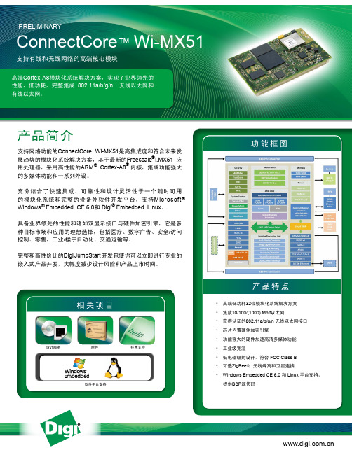
产品特点• 高端低功耗32位模块化系统解决方案• 集成10/100/(1000) Mbit 以太网• 获得认证的802.11a/b/g/n 无线以太网接口• 芯片内置硬件加密引擎• 功能强大的硬件加速高清多媒体功能• 工业级宽温 • 低电磁辐射设计,符合 FCC Class B• 可选ZigBee ,无线蜂窝和卫星连接• Windows Embedded CE 6.0 和 Linux 平台支持,支持有线和无线网络的高端核心模块设计服务技术支持软件平台支持ConnectCore ™ Wi-MX51PRELIMINARY高端Cortex-A8模块化系统解决方案,实现了业界领先的性能,低功耗,完整集成 802.11a/b/g/n 无线以太网和有线以太网。
支持网络功能的ConnectCore Wi-MX51是高集成度和符合未来发展趋势的模块化系统解决方案,基于最新的Freescalei.MX51 用处理器,采用高性能的ARM Cortex-A8 内核,集成功能强大的多媒体功能和一系列外设。
充分结合了快速集成、可靠性和设计灵活性于一个随时可用的模块化系统和完整的设备外软件开发平台,支持Microsoft Windows Embedded CE 6.0和 Digi Embedded Linux 。
具备业界领先的性能和诸如双显示接口与硬件加密引擎,它是多种目标市场和应用的理想选择,包括医疗、数字广告、安全控制、零售,工业/楼宇自动化、交通运输等。
完整和高性价比的Digi JumpStart 开发包使你可以立即进行专业的嵌入式产品开发,大幅度减少设计风险和产品上市时间。
®®®®®®产品简介开发包天 Visual Studio 2005和Windows Embedded CE 6.0 评测版Freescale i.MX51600/800 MHz •处理器型号主频模块特点•不是所有信号都同时可用,有些管脚是复用的。
51mx37m椭圆形网架结构全套施工图

筒仓外壁聚氨酯硬质泡沫保温防水施工工法
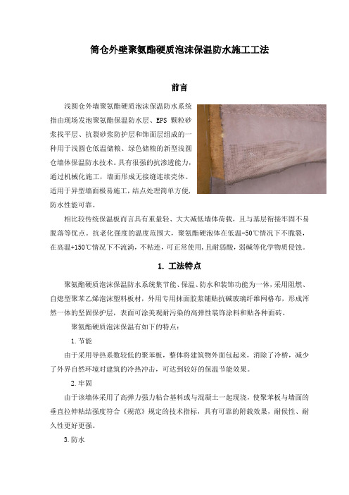
筒仓外壁聚氨酯硬质泡沫保温防水施工工法前言浅圆仓外墙聚氨酯硬质泡沫保温防水系统指由现场发泡聚氨酯保温防水层、EPS颗粒砂浆找平层、抗裂砂浆防护层和饰面层组成的一种用于浅圆仓低温储粮、绿色储粮的新型浅圆仓墙体保温防水技术。
具有很强的抗渗透能力,通过机械化施工,墙面形成无接缝连续壳体。
适用于异型墙面极易施工,结点处理简单方便,防水性能可靠。
相比较传统保温板而言具有重量轻、大大减低墙体荷载,且与基层衔接牢固不易脱落等优点。
抗老化强度的温度范围大,聚氨酯硬泡体在低温-50℃情况下不脆裂,在高温+150℃情况下不流淌,不粘连,可正常使用,且耐弱酸,弱碱等化学物质侵蚀。
1.工法特点聚氨酯硬质泡沫保温防水系统集节能、保温、防水和装饰功能为一体,采用阻燃、自熄型聚苯乙烯泡沫塑料板材,外用专用抹面胶浆铺贴抗碱玻璃纤维网格布,形成浑然一体的坚固保护层,表面可涂美观耐污染的高弹性装饰涂料和贴各种面砖。
聚氨酯硬质泡沫保温有如下的特点:1.节能由于采用导热系数较低的聚苯板,整体将建筑物外面包起来,消除了冷桥,减少了外界自然环境对建筑的冷热冲击,可达到较好的保温节能效果。
2.牢固由于该墙体采用了高弹力强力粘合基料或与混凝土一起现浇,使聚苯板与墙面的垂直拉伸粘结强度符合《规范》规定的技术指标,具有可靠的附载效果,耐候性、耐久性更好更强。
3.防水该墙体具有高弹性和整体性,解决了墙面开裂,表面渗水的通病,特别对陈旧墙面局部裂纹有整体覆盖作用。
4.体轻采用该材料可将建筑房屋外墙厚度减小,不但减小了砌筑工程量、缩短工期,而且减轻了建筑物自重。
5.阻燃材料为阻燃型,具有隔热、无毒、自熄、防火功能。
6.易施工该墙体饰面施工,对建筑物基层混凝土、红砖、砌块、石材、石膏板等有广泛的适用性。
施工简单的工具,具有一般抹灰水平的技术工人,经短期培训,即可进行现场操作施工。
2.适用范围适用于由低温储粮要求的仓储类浅圆仓以及平房仓;同时适用于有保温要求的异性工业与民用建筑的墙面、屋面。
安可信智能手机及平板电脑项目简介
高通公司2010年中国合作伙伴大会暨创新无线终端联合展示
电子工程世界评出的2011最值得期待的八款手机公板
平板电脑
平板电脑已被市场高度认同
iPad发布销售仅两日,销量就达到了惊人的45 万台,第四季度单季销量已达733万台。 而从去年三季度开始,Google Android操作系 统已在手机、平板电脑等便携设备领域超越苹果, 成为3G智能终端新霸主。采用Google Android操作 系统的各类智能终端如日中天,仅仅间隔3个月, 销量便由20万台/天增加到30万台/天,震惊业界。 市场正在有力的证明着这一处于智能手机和笔记本 中间态的新产品-平板电脑的广阔前景。 权威机构预测: 3G平板电脑的出现,将覆盖电子书,MID,上 网本等市场。
团队核心 沈强 :成都理工大学 应用电子专业 主要经历: 核工业216 核辐射探测仪器数据采集部分的研发 西门子,基站工程部 技术支持工程师 DBTEl 产品经理 主要负责摩托罗拉系列在dbtel的产品整合 2002-2007中兴通讯02年协助李溯副总完成中兴通讯手机制造中心的规划筹 建,在03年7月1号年产1800万只手机基地建设完成投产 ,从规划,基建, 人员招聘,设备安装调试到正式投产,只用了9个月时间。 2003-2007 组织筹建手机事业部国际业务部,任国际业务部部长,牵头组 织完成巴西VIVO CDMA手机项目,英国和黄3G手机项目,沃达丰GSM 手机项目,印度TATA CDMA项目等多个重要里程碑项目,中兴手机国际 市场销售额2007年完成10亿美金 2007-2010 昱为科技手机事业部总经理 2010年9月加入安可信 负责产品运作及销售
MSM7227的平板电脑I700T ,在2011年5月,即将推出基于 年 月 Qualcomm Snapdragon的平板电脑 的平板电脑I880 。
安卓平板方案
1.产品规划
-硬件配置:选择主流的高通或联发科处理器,配备至少4GB RAM和64GB存储空间,提供10.1英寸以上高清显示屏。
-外观设计:采用轻薄设计,便于携带,同时保证良好的散热性能。
-电池续航:内置大容量电池,确保长时间的使用需求。
2.系统定制
-操作系统:基于最新版本的Android操作系统进行定制,优化系统性能和电池使用效率。
安卓平板方案
第1篇
安卓平板方案
一、项目背景
随着移动互联网的迅猛发展,安卓平板作为一种便捷的移动设备,广泛应用于各类场景,如教育、企业办公、家庭娱乐等。为满足日益增长的市场需求,提供高效、稳定、安全的安卓平板解决方案至关重要。
二、目标定位
1.提供具备高性价比的安卓平板产品。
2.确保系统安全稳定,用户体验优良。
3.符合我国相关法律法规,合法合规经营。
三、方案设计
1.产品选型
-选用主流品牌厂商生产的安卓平板,确保产品质量和售后服务。
-根据市场需求,提供多种配置供用户选择,包括但不限于:处理器、内存、存储、屏幕尺寸等。
2.系统定制
-基于原生安卓系统进行定制,优化用户体验。
-预装符合我国法律法规的必要应用,如办公软件、学习软件等。
4.服务与支持
-售后服务:提供快速响应的售后服务,包括硬件维修、系统更新等。
-用户培训:组织线上线下用户培训活动,帮助用户更好地使用产品。
5.合规性管理
-法律法规遵循:确保产品符合国家法律法规,如网络安全法、个人信息保护法等。
-质量监管:通过国家强制认证,确保产品质量。
四、实施流程
1.市场调研:收集用户需求,分析竞争对手,确定产品定位。
4.风险:合规性风险。
全志平板方案
6.生产交付:严格控制产品质量,确保按时交付。
八、风险控制
1.技术更新:关注行业技术动态,确保产品技术领先;
2.市场变化:及时调整产品策略,适应市场变化;
3.法律法规:加强合规性监控,防范法律风险;
4.售后服务:提高服务质量,降低售后风险。
九、结论
全志平板方案以用户需求为核心,通过严谨的硬件选型、软件部署、服务支持及合规性保障,致力于提供高效、合规的平板电脑产品。在实施过程中,将持续关注市场动态,积极应对各种风险,为用户提供优质的产品和服务体验。
3.服务与支持
(1)售后服务:提供全国联保、在线客服、电话支持等服务;
(2)技术支持:提供系统升级、驱动下载、使用教程等技术支持;
(3)培训与指导:为企业、学校等用户提供培训与指导服务。
四、合法合规性
1.硬射设备型号核准等;
2.软件合规性:确保软件产品符合国家相关法律法规,如计算机软件保护条例、网络安全法等;
全志平板方案
第1篇
全志平板方案
一、项目背景
随着移动互联网的普及,平板电脑已成为人们日常生活、工作中不可或缺的智能设备。全志科技作为国内领先的平板处理器制造商,致力于为用户提供高性能、低功耗的平板解决方案。本方案旨在为全志平板用户提供一套合法合规的方案,以满足其在不同场景下的需求。
二、目标用户
1.企业用户:用于商务演示、会议记录、企业培训等场景;
5.合规性审查:确保方案符合国家法律法规;
6.生产与交付:完成生产,确保产品品质,及时交付用户。
六、风险评估与应对措施
1.技术风险:积极跟进新技术动态,确保产品技术领先;
2.市场风险:深入了解市场需求,调整产品策略;
EXT-SBC-i.MX51-EXP V2.0 用户手册说明书

ContactBluetechnix Mechatronische Systeme GmbH Waidhausenstraße 3/19A-1140 ViennaAUSTRIA/EUROPE*********************Document No.: 100-2520-2.4Date: 2011-08-04i.MX Core Modules (5)Core Module naming information (6)i.MX Development Boards (7)1Introduction (8)1.1Overview (8)2PIN Description (9)2.1I/O Power Domain Overview (9)2.2Pin Location (9)3Operating Conditions (13)3.1Power Supplies (13)3.2Digital I/O Characteristics (13)3.3Analog Inputs (14)3.3.1ESD Sensitivity (14)4Mechanical Outline (15)5Support (16)5.1General Support (16)5.2Board Support Packages (16)5.3i.MX Software Support (16)5.3.1Linux (16)5.3.2Win CE (16)5.4i.MX® Design Services (16)5.4.1Upcoming Products and Software Releases (16)6Ordering Information (17)6.1Predefined mounting options for EXT-SBC-i.MX51-EXP (17)7Dependability (18)7.1MTBF (18)8Product History (19)8.1Version Information (19)8.2Anomalies (19)9Document Revision History (20)10List of Abbreviations (21)A List of Figures and Tables (22)The information herein is given to describe certain components and shall not be considered as a guarantee of characteristics.Terms of delivery and rights of technical change reserved.We hereby disclaim any warranties, including but not limited to warranties of non-infringement, regarding circuits, descriptions and charts stated herein.Bluetechnix makes and you receive no warranties or conditions, express, implied, statutory or in any communication with you. Bluetechnix specifically disclaims any implied warranty of merchantability or fitness for a particular purpose.Bluetechnix takes no liability for any damages and errors causing of the usage of this board. The user of this board is responsible by himself for the functionality of his application. He is allowed to use the board only if he has the qualification. More information is found in the General Terms and Conditions (AGB).InformationFor further information on technology, delivery terms and conditions and prices please contact Bluetechnix ().WarningDue to technical requirements components may contain dangerous substances.CM-i.MX27-C-C-Q26S128F32N512The Core Module CM-i.MX27 is powered by Freescales' SoC i.MX27 (ARM 926 core, up to 400MHz). It addresses 128MB DDR-RAM, has an onboard NOR-flash of 32MByte and a NAND-flash with 512MByte at a size of 55x45mm. CM-i.MX31-C-C-Q26S128F40N128-EThe Core Module CM-i.MX31 is powered by Freescales' SoC i.MX31 (ARM1136JF-S core, up to 532MHz). It addresses 128MB DDR-RAM, has an onboard NOR-flash of 40MByte and a NAND-flash with 128MByte at a size of 55x45mm. Core module is available as connector or BGA.CM-i.MX53-C-I-Q24S1024F4N2048)The Core Module CM-i.MX53 is powered by Freescales' SoC i.MX53 (ARM® Cortex™-A8, up to 1GHz). It addresses 1024MB DDR2-SDRAM, has an onboard NOR-flash of 4MByte and a NAND-flash with 2048MByte at a size of 80x45mm.The idea is to put more Core Module specific technical information into the product name. New Core Module names will have following technical information covered in their names.•Product Family,•CPU-Type,•Connection-Type,•Operating Temperature Range,•Crystal Frequency [MHz],•RAM [MB],•Flash [MB],•External ControllersOptional•o Special and/oro Former nameThat expands of course the name but allows the customer to get the most important Core Module specific information at the first sight. Have a look at the example below to get an idea of the new Core Module names. Example CM-BF537-C-C-Q25S32F4 (CM-BF537E)DEV-i.MX27The DEV-i.MX27 development board is an extendable development platform for the CM-i.MX27 processor modules. With display connector and keypad it can be used as a reference design for a low power mobile handheld device powered by a single Lithium Ion battery. The development board provides all interfaces of the connector version on dedicated expansion connectors. Extender boards can be plugged on top of the development board in order to enable additional interfaces.DEV-iMX31The DEV-i.MX31 Development Board is an extendable development platform for the CM-i.MX31 processor module. With display connector and keypad it can be used as a reference design for a low power mobile handheld device powered by a single Lithium Ion battery. The development board provides all interfaces of the connector version on dedicated expansion connectors. Extender boards can be plugged on top of the development board in order to enable additional interfaces.SBC-i.MX51-S-C-Q24S512N2048The Single-Board Computer SBC-i.MX51 is based on Freescale’s high-performance i.MX51 mobile platform, incorporating an ARM Cortex-A8 CPU, an Image Processing Unit (IPUv3EX), a Video Processing Unit (VPU) and a Graphical Processing Unit (GPU). The IPUv3EX provides comprehensive support for connectivity to displays and cameras. The VPU supports hardware encoding and decoding of MPEG-4, H.263, H.264 and many more standards. The GPU serves 3D and 2Dacceleration in hardware. The board‘s memory capabilities (NAND Flash, DDR2) and numerous interfaces like Ethernet, HDMI,4xUSB and USB-OTG turn the SBC-i.MX51 into the ultimate development board for future high-end embedded devices.DEV-i.MX53The DEV-i.MX53 development board is an extendable development platform for the CM-i.MX53 processor module. The development board provides all interfaces of the connector version (Ethernet, HDMI,4xUSB and USB-OTG) on dedicated extender connectors. Extender boards can be plugged on top of the development board in order to enable additional interfaces.Extender boardsExtender boards (EXT-SBC-i.MX51-) are expanding the development board SBC-i.MX51 by several interfaces and functionalities. Targeted application areas are: audio/video processing, security and surveillance, Ethernet access, positioning, automation and control, experimental development and measuring.Note! Bluetechnix is offering tailored board developments as well.1.1OverviewThe primary goal of the EXT-SBC-i.MX51-EXP is to ensure easy connection of separate hardware with the SBC-i.MX51. Each extender connector pin is routed to a solder pad on the EXT-SBC-i.MX51-EXP. The USB-Hosts can be accessed via micro USB- connectors. The Pads are ordered in a 2.54mm pitch spacing to ensure that standard thru-hole headers or sockets can be easily soldered.Figure 1-1: Connected EXT-SBC-i.MX51-EXP on SBC-i.MX512.1I/O Power Domain OverviewAll digital I/O pins belong to one of three available power domains: P_SW4 (1.8V), P_VIOHI (2.775V) or P_GEN2 (3.15V). The following table shows each interface with the corresponding voltage level.I²C2 2 P_VIOHI I2C1.SCL, I2C1.SDAKeypad 10 P_SW4 KPP.COL[0..5], KPP.ROW[0..3]PWM 2 P_VIOHI PWM1, PWM2SD 6 P_GEN2 SD2.CMD, SD2.CLK, SD2.D0, SD2.D1, SD2.D2, SD2.D3SPI 6 P_SW4 CSPI1.MOSI, CSPI1.MISO, CSPI1.SS0, CSPI1.SS1, CSPI1.RDY, CSPI1.SCLK SSI 6 P_VIOHI AUD4.RFS, AUD4.RSCK, AUD4.Tx, AUD4.Rx, AUD4.TSCK, AUD4.TFS UART 4 P_VIOHI UART2.TXD, UART2.RXD, UART3.TXD, UART3.RXDPON 1 Open Drain A_CTRL.PON1 – Power down Power Mgmt.ADIN 3 - ADC Input on MC13892Table 2-1: Power Domains for I/Os2.2Pin LocationFigure 2-1: Pin location23 I2C2_SCL O P_VIOHI usable as I2C2_SCL or GPIO2_94 I2C2_SDA IO P_VIOHI usable as I2C2_SDA or GPIO2_85 OWIRE IO P_VIOHI One-Wire Interface6 RxD2 I P_VIOHI UART2 RxD or GPIO 1_207 TxD2 O P_VIOHI UART2 TxD or GPIO 1_218 RxD3 I P_VIOHI UART3 RxD or GPIO 1_229 TxD3 O P_VIOHI UART3 TxD or GPIO 1_2310 GPIO1.9 IO P_VIOHI General Purpose Input or Output11 GPIO1.8 IO P_VIOHI General Purpose Input or Output12 GPIO1.6 IO P_VIOHI General Purpose Input or Output13 PWM1 IO P_VIOHI GPIO1_2 with PWM1 functionality14 PWM2 IO P_VIOHI GPIO1_3 with PWM2 functionality15 ROW0 I P_SW4 Keypad Row16 ROW1 I P_SW4 Keypad Row17 ROW2 I P_SW4 Keypad Row18 ROW3 I P_SW4 Keypad Row19 COL0 I P_SW4 Keypad Column20 COL1 I P_SW4 Keypad Column21 COL2 I P_SW4 Keypad Column22 COL3 I P_SW4 Keypad Column23 COL4 I P_SW4 Keypad Column24 COL5 I P_SW4 Keypad Column25 P_MLB PWR P_MLB Power Supply26 P_SW4 PWR P_SW4 Power Supply27 P_EXT PWR P_EXT Power Supply28 P_VIOHI PWR P_VIOHI Power Supply29 GND PWR GND Power Ground30 P_5V0 PWR P_5V0 Power Supply31 P_SWLED PWR P_SWLED Power Supply32 GND PWR GND Power Ground33 LED.AD O P_SWLED LED driver output connected to MC1839234 LED.KP O P_SWLED LED driver output connected to MC1839235 ADIN5 I Analog input connected to MC1839236 ADIN6 I Analog input connected to MC1839237 ADIN7 I Analog input connected to MC1839238 P_GEN2 PWR P_GEN2 Power Supply39 SD2.CMD IO P_GEN2 SD-card interface or CSPI_MOSI40 SD2.CLK O P_GEN2 SD-card interface or CSPI_SCLK41 SD2.D0 IO P_GEN2 SD-Card Interface42 SD2.D1 IO P_GEN2 SD- Card Interface43 SD2.D2 IO P_GEN2 SD- Card Interface44 SD2.D3 IO P_GEN2 SD- Card Interface or CSPI_SS245 SCLK IO P_SW4 SPI1 usable as I2C1_SCL or GPIO4_2746 MOSI IO P_SW4 SPI1 usable also as I2C1_SDA or GPIO4_2247 MISO I P_SW4 SPI1 usable also as GPIO4_2348 CS0 O P_SW4 SPI1 usable also as GPIO4_2449 CS1 O P_SW4 SPI1 usable also as GPIO4_2550 RDY I P_SW4 SPI1 usable also as GPIO4_2651 RFS IO P_VIOHI Audio Port 4 usable also as GPIO2_052 RSCK IO P_VIOHI Audio Port 4 usable also as GPIO2_35455 TSCK IO P_VIOHI Audio Port 4 usable also as GPIO2_656 TFS IO P_VIOHI Audio Port 4 usable also as GPIO2_757 GND PWR GND Power Ground58 GND PWR GND Power Ground59 DD2 O P_VIOHI Display Port 2 Data60 DD0 O P_VIOHI Display Port 2 Data61 DD6 O P_VIOHI Display Port 2 Data62 DD4 O P_VIOHI Display Port 2 Data63 DD10 O P_VIOHI Display Port 2 Data64 DD8 O P_VIOHI Display Port 2 Data65 DD14 O P_VIOHI Display Port 2 Data66 DD12 O P_VIOHI Display Port 2 Data67 DVSYNC O P_VIOHI Display Port 3 VSYNC68 DCLK O P_VIOHI Display Port 2 Clock69 LED.MD O P_SWLED LED driver output connected to MC1839270 GPIO3.5 IO P_SW4 General Purpose Input or Output71 ADIN4 I Analog input for touch pad usage connected to MC18392 73 CD1 I P_SW4 CMOS Sensor Interface 1 Data72 DPCI IO P_VIOHI Usable as GPIO2_2074 ADIN3 I Analog input for touch pad usage connected to MC1839275 CD5 I P_SW4 CMOS Sensor Interface 1 Data76 CD3 I P_SW4 CMOS Sensor Interface 1 Data77 CD9 I P_SW4 CMOS Sensor Interface 1 Data78 CD7 I P_SW4 CMOS Sensor Interface 1 Data79 MCLK O P_SW4 CMOS Sensor Interface 1 Master Clock80 PCLK I P_SW4 CMOS Sensor Interface 1 Pixel Clock81 P_SW4 PWR P_SW4 Power Supply82 P_DIG PWR P_DIG Power Supply83 P_VIOHI PWR P_VIOHI Power Supply84 P_3V3 PWR P_3V3 Only available if 3V3 regulator is populated on SBC i.MX5185 DD3 O P_VIOHI Display Port 2 Data86 DD1 O P_VIOHI Display Port 2 Data87 DD7 O P_VIOHI Display Port 2 Data88 DD5 O P_VIOHI Display Port 2 Data89 DD11 O P_VIOHI Display Port 2 Data90 DD9 O P_VIOHI Display Port 2 Data91 DD15 O P_VIOHI Display Port 2 Data92 DD13 O P_VIOHI Display Port 2 Data93 DDE O P_SW4 Display Port 4 Data Enable94 DHSYNC O P_VIOHI Display Port 2 HSYNC95 GPIO3.7 IO P_SW4 Usable as GPIO3_796 GPIO3.6 IO P_SW4 Usable as GPIO3_697 PWM1 IO P_VIOHI GPIO1.2 with PWM functionality98 GPIO3.8 IO P_SW4 Usable as GPIO3_899 ADIN1 I Analog input for touch pad usage connected to MC18392 100 ADIN2 I Analog input for touch pad usage connected to MC18392 101 SCL1 IO P_SW4 usable as I2C1_SCL for cam configuration or GPIO4_27 102 SDA1 IO P_SW4 usable as I2C1_SDA for cam configuration or GPIO4_22 103 CD0 I P_SW4 CMOS Sensor Interface 1 Data104 CD2 I P_SW4 CMOS Sensor Interface 1 Data106107 CD8 I P_SW4 CMOS Sensor Interface 1 Data108 CVSYNC I P_SW4 CMOS Sensor Interface 1 VSYNC109 CHSYNC I P_SW4 CMOS Sensor Interface 1 HSYNC110 CPCI O P_SW4 usable as GPIO3_12 (e.g. Power Down) 111 P_CAM PWR P_CAM Power Supply112 P_GEN3 PWR P_GEN3 Power Supply113 GND PWR GND Power Ground114 P_5V0 PWR P_5V0 Power SupplyTable 2-2: Pin descriptionThis section provides the operating conditions for the EXT-SBC-i.MX51-EXP Extender Board.3.1Power SuppliesThe EXT-SBC-i.MX51-EXP provides different supply voltages. They can be used to supply custom electronics. Some supply voltages are generated by the MC13892 PMIC and can be set to different values. They must be set and enabled first by configuring the companion IC. The following table shows the maximum supply current for each voltage domain.P_3V3 3.3V 500mAP_VIOHI1) 2.775V 50mAP_SW41) 1.8V 50mAP_GEN21) 3.15V 70mAP_GEN3 1.8V, 2.9V 50mAP_DIG 1.05V, 1.25V, 1.65V, 1.8V 50mAP_CAM 2.5V, 2.6V, 2.75V, 3.0V 250mAP_EXT3) 2.3V, 2.5V, 2.775V, 3.0V 150mAP_MLB3) 2.5V, 2.6V, 2.7V, 2.775V 350mATable 3-1: Maximum power consumption for the GPIO / Automation Connector supplies1) It is not advisable to alter these voltages; otherwise the board may get damaged.2) The P_SWLED voltage drives the LEDs connected to the LED-driver pins. The output voltage will be set automatically by the MC13892. Please also refer to the MC13892 errata sheet available from the Freescale website.3) P_EXT is called VAUDIO and P_MLB is called VVIDEO on the MC13892 Users Guide.3.2Digital I/O CharacteristicsMost IO pins available on the Extension Connectors (X3 and X11) are connected to the i.MX, and are assigned to one of three power domains.High-Level Output Voltage PGEN2 V ohHigh-Level Output Voltage P_SW4 V oh 1.65 1.8 2.1 VLow-Level Output Voltage all domains V ol- - 0.15 VHigh Level Output Current all domains I oh 1.9 - 6.6 mA Low-Level Output Current all domains I ol 1.9 - 6.6 mA High-Level Input Voltage P_VIOHI V ih 1.95 - 2.775 VLow -Level Input Voltage P_VIOHI V il0 - 0.83 VHigh-Level Input Voltage PGEN2 V ih 2.21 - 3.15 VLow-Level Input Voltage PGEN2 V il0 - 0.94 VHigh -Level Input Voltage P_SW4 V ih 1.26 - 1.8 VLow -Level Input Voltage P_SW4 V il0 - 0.54 VTable 3-2: Digital IO characteristicsThe 10-bit ADC which is integrated in the MC13892 allows measuring analog voltages. These analog inputs are mainly used for touchpad sensing or voltage (battery) monitoring.Conversion Current I cConversion Core Input Voltage V in0 - 2.4 V Conversion Time Per Channel t c10 µsTable 3-3: ADC characteristics3.3.1ESD SensitivityESD (electrostatic discharge) sensitive device. Charged devices and circuit boards candischarge without detection. Although this product features patented or proprietaryprotection circuitry, damage may occur on devices subjected to high energy ESD.Therefore, proper ESD precautions should be taken to avoid performance degradation orloss of functionality.This section shows the position of all connectors and mounting holes. All dimensions are given in mm.Figure 4-1: EXT-SBC-i.MX51-EXP top view5.1General SupportGeneral support for products can be found at Bluetechnix’ support site https://support.bluetechnix.at/wiki5.2Board Support PackagesBoard support packages, boot loaders and further software downloads can be downloaded at the products wiki page at https://support.bluetechnix.at/wiki5.3i.MX Software Support5.3.1LinuxLinux BSP and images of derivates can be found at Bluetechnix’ support site https://support.bluetechnix.at/wiki at the software section of the related product.5.3.2Win CEWinCE is only supported on ARM platforms. Please contact Bluetechnix for support information.5.4i.MX® Design ServicesBased on more than seven years of experience with Blackfin and i.MX, Bluetechnix offers development assistance as well as custom design services and software development.5.4.1Upcoming Products and Software ReleasesKeep up to date with all product changes, releases and software updates of Bluetechnix at .6.1Predefined mounting options for EXT-SBC-i.MX51-EXP(SBC-i.MX51)Table 6-1: Ordering informationNOTE:Custom hard and software developments are available on request! Please contact Bluetechnix (**********************) if you are interested in custom hard- and software developments.7.1MTBFPlease keep in mind that a part stress analysis would be the only way to obtain significant failure rate results, because MTBF numbers just represent a statistical approximation of how long a set of devices should last before failure. Nevertheless, we can calculate an MTBF of the development board using the bill of material. We take all the components into account. The PCB and solder connections are excluded from this estimation. For test conditions we assume an ambient temperature of 30°C of all development board components. We use the MTBF Calculator from ALD (/) and use the reliability prediction MIL-217F2 Part Stress standard. Please get in touch with Bluetechnix (**********************) if you are interested in the MTBF result.8.1Version Information1.0 2010-12-22 First extender board release.Table 8-1: Overview product changes 8.2Anomalies3 2011 04 20 Changed description of Pin 842 2011 03 17 Update for Board Revision V2.0.1 2010 12 22 First draft release.Table 9-1: Revision historyAI Analog InputAMS Asynchronous Memory SelectAO Analog OutputCM Core ModuleDC Direct CurrentDSP Digital Signal ProcessoreCM Enhanced Core ModuleEBI External Bus InterfaceESD Electrostatic DischargeGPIO General Purpose Input OutputI InputI²C Inter-Integrated CircuitI/O Input/OutputISM Image Sensor ModuleLDO Low Drop-Out regulatorMTBF Mean Time Between FailureNC Not ConnectedNFC NAND Flash ControllerO OutputOS Operating SystemPPI Parallel Peripheral InterfacePWR PowerRTOS Real-Time Operating SystemSADA Stand Alone Debug AgentSD Secure DigitalSoC System on ChipSPI Serial Peripheral InterfaceSPM Speech Processing ModuleSPORT Serial PortTFT Thin-Film TransistorTISM Tiny Image Sensor ModuleTSC Touch Screen ControllerUART Universal Asynchronous Receiver TransmitterUSB Universal Serial BusUSBOTG USB On The GoTable 10-1: List of abbreviationsFiguresFigure 1-1: Connected EXT-SBC-i.MX51-EXP on SBC-i.MX51 (8)Figure 2-1: Pin location (9)Figure 4-1: EXT-SBC-i.MX51-EXP top view (15)TablesTable 2-1: Power Domains for I/Os (9)Table 2-2: Pin description (12)Table 3-1: Maximum power consumption for the GPIO / Automation Connector supplies (13)Table 3-2: Digital IO characteristics (13)Table 3-3: ADC characteristics (14)Table 6-1: Ordering information (17)Table 8-1: Overview product changes (19)Table 8-2: Overview product anomalies (19)Table 9-1: Revision history (20)Table 10-1: List of abbreviations (21)Mouser ElectronicsAuthorized DistributorClick to View Pricing, Inventory, Delivery & Lifecycle Information:B ECOM:100-2520-2。
- 1、下载文档前请自行甄别文档内容的完整性,平台不提供额外的编辑、内容补充、找答案等附加服务。
- 2、"仅部分预览"的文档,不可在线预览部分如存在完整性等问题,可反馈申请退款(可完整预览的文档不适用该条件!)。
- 3、如文档侵犯您的权益,请联系客服反馈,我们会尽快为您处理(人工客服工作时间:9:00-18:30)。
性能最稳定的Cortex A8平板电脑整机方案
作为飞思卡尔(Freescale)官方认证的第三方设计公司,辰汉电子(Morninghan)一直专注于i.MX系列产品的研发和应用,是国内最具权威的i.MX产品方案专家。
并且在国内领先推出基于i.MX51的平板电脑整机方案,凭借辰汉电子(Morninghan)深厚的研发实力,和成熟稳定的平板电脑方案,成为联想(Lenovo)ThinkPad系列商务平板电脑的方案供应商。
辰汉电子(Morninghan)倾力打造的基于ARM Cortex A8 i.MX51平板电脑MiPad经过多方测试稳定性极佳,整机功耗极低,精选高品质耐用电池,视频持续播放时间达到8—10小时,StandBy待机时间长达5—7天。
优化加强版的Android 2.2操作系统,我们解决了很多系统性Bug,可以更流畅的调用i.MX515芯片的2D、3D图形硬件加速器,极速运行3D游戏、Flash上网、高清视频播放等高级别应用。
数十万应用程序随你畅玩,可预装定制化应用程序商店,精选国内主流优质应用程序,满足本土化应用下载需求。
源自全球技术领先的美国飞思卡尔(原摩托罗拉半导体公司)的Cortex A8 高性能处理器MX51被认定为目前性能最强、产品最稳定、成熟的平板电脑处理器之一。
辰汉电子MiPad整机TP电容屏为双层全进口钢化玻璃,强度大,透光率高,液晶屏采用韩国LG IPS液晶屏(全球技术领先的硬屏,与Apple iPad液晶屏规格相同)。
版贴iNand Flash解决方案—4G、8G、16G任你选择,避免内置TF卡方式的不稳定隐患,是走中高端平板电脑的最佳选择。
同时拥有丰富的接口应用:BT蓝牙语音控制+数据传输、HDMI高清视频输出、USB OTG、USB Host鼠标U盘随时插接、TF卡更大容量扩展存储、Wifi/3G版本任意选择。
辰汉为您提供性价比最高、性能最稳定的平板电脑整机方案。
详细参数:
Title
Cortex A8 平板电脑方案
平板电脑的机遇和挑战
2011年最好的平板电脑方案2011年平板电脑何去何从
平板电脑的核心竞争力在哪里?现在平板电脑最缺什么?
平板电脑的发展之路
平板电脑何去何从?。