M93S46-WDS6T中文资料
各主流品牌电脑数据
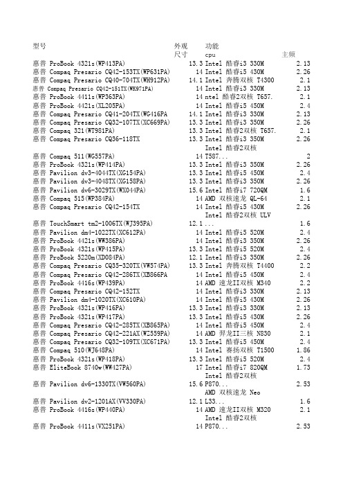
型号外观功能尺寸cpu主频惠普 ProBook 4321s(WP413PA) 13.3Intel 酷睿i3 330M 2.13惠普 Compaq Presario CQ42-153TX(WP631PA)14Intel 酷睿i5 430M 2.26惠普 Compaq Presario CQ40-704TX(WH912PA) 14.1Intel 奔腾双核 T4300 2.1惠普 Compaq Presario CQ42-151TX(WK971PA)14Intel 酷睿i3 330M 2.13惠普 ProBook 4411s(WP363PA) 14ntel 酷睿2双核 T657. 2.1惠普 ProBook 4421s(XL205PA) 14Intel 酷睿i5 450M 2.4惠普 Compaq Presario CQ41-204TX(WG416PA14.1Intel 酷睿i3 330M 2.13惠普 Compaq Presario CQ32-107TX(XC669PA)13.3Intel 酷睿i3 350M 2.26惠普 Compaq 321(WT981PA) 13.3Intel 酷睿2双核 T657. 2.1惠普 Compaq Presario CQ36-118TX13.3Intel 酷睿i3 350M 2.26惠普 Compaq 511(WG557PA) 14Intel 酷睿2双核 T587 (2)惠普 ProBook 4321s(WP414PA) 13.3Intel 酷睿i3 350M 2.26惠普 Pavilion dv3-4044TX(XG154PA) 13.3Intel 酷睿i5 450M 2.4惠普 Pavilion dv3-4048TX(XG158PA)13.3Intel 酷睿i3 350M 2.26惠普 Pavilion dv6-3029TX(WX044PA) 15.6Intel 酷睿i7 720QM 1.6惠普 Compaq 515(WP384PA)14AMD 双核速龙 QL-64 2.1惠普 Compaq Presario CQ42-154TX14Intel 酷睿i5 430M 2.26惠普 TouchSmart tm2-1006TX(WJ395PA)12.1Intel 酷睿2双核 ULV ... 1.6惠普 Pavilion dm4-1022TX(XC612PA)14Intel 酷睿i5 520M 2.4惠普 ProBook 4421s(WW386PA)14Intel 酷睿i3 350M 2.26惠普 ProBook 4321s(WP415PA)13.3Intel 酷睿i5 520M 2.4惠普 ProBook 5220m(XD084PA)12.1Intel 酷睿i3 350M 2.26惠普 Compaq Presario CQ35-320TX(VW574PA)13.3Intel 奔腾双核 T4400 2.2惠普 Compaq Presario CQ42-286TX(XB866PA14Intel 酷睿i5 450M 2.4惠普 ProBook 4416s(WP439PA)14AMD 速龙II双核 M340 2.2惠普 Compaq Presario CQ42-152TX14Intel 酷睿i3 330M 2.13惠普 Pavilion dm4-1020TX(XC610PA)14Intel 酷睿i5 430M 2.26惠普 ProBook 4321s(WP416PA)13.3Intel 酷睿i3 330M 2.13惠普 ProBook 4321s(WP417PA)13.3Intel 酷睿i5 430M 2.26惠普 Compaq Presario CQ42-285TX(XB865PA)14Intel 酷睿i5 450M 2.4惠普 Compaq Presario CQ42-221AX(WZ559PA)14AMD 羿龙II三核 N830 2.1惠普 Compaq Presario CQ32-109TX(XC671PA)13.3Intel 酷睿i5 450M 2.4惠普 Compaq 510(WJ648PA)14Intel 赛扬双核 T1500 1.86惠普 ProBook 4321s(WP418PA)13.3Intel 酷睿i5 520M 2.4惠普 EliteBook 8740w(WW427PA)17Intel 酷睿i7 820QM 1.73惠普 Pavilion dv6-1330TX(VW560PA)15.6Intel 酷睿2双核 P870... 2.53惠普 Pavilion dv2-1201AX(VV330PA)12.1AMD 双核速龙 Neo L33... 1.6惠普 ProBook 4416s(WP440PA)14AMD 速龙II双核 M320 2.1惠普 ProBook 4411s(VX251PA)14Intel 酷睿2双核 P870... 2.53惠普 ProBook 4710s(WH401PA)17.3Intel 酷睿2双核 T657.. 2.1惠普 Compaq Presario CQ42-283TX(XB863PA)14Intel 奔腾双核 P6000 1.86惠普 Pavilion dm1-1119TU(WJ389PA)11.6Intel 奔腾双核 ULV S... 1.3惠普 Compaq Presario CQ42-251TX(WY332PA)14Intel 酷睿i3 350M 2.26惠普 Compaq Presario CQ42-219AX14AMD 羿龙II四核 N9302惠普 Compaq Presario CQ35-222TX(VH112PA)13.3Intel 奔腾双核 T4300 2.1惠普 ProBook 6450b(XD150PA)14Intel 酷睿i3 350M 2.26惠普 Pavilion dv6-3028TX(WX043PA)15.6Intel 酷睿i5 520M 2.4惠普 EliteBook 2540p(WT759PA)12.1Intel 酷睿i5 540M 2.53惠普 EliteBook 2540p(VB715AV)12.1Intel 酷睿i5 520M 2.4惠普 Pavilion dv3-4045TX(XG155PA)13.3Intel 酷睿i7 720QM 1.6惠普 Compaq Presario CQ32-105TX(XC667PA) 13.3Intel 奔腾双核 P6000 1.86东芝 Satellite L600-03R 14Intel 酷睿i3 330M 2.13东芝 Satellite L600-25R14Intel 酷睿i3 350M 2.26东芝 Portege R700-01B 13.3Intel 酷睿i3 350M 2.26东芝 Satellite L600-23W 14Intel 酷睿i3 350M 2.26东芝 Satellite L630-05R13.3Intel 奔腾双核 P6000 1.86东芝 Satellite L600-05S 14Intel 酷睿i5 430M 2.26东芝 Satellite P505(i7 720QM) 18.4Intel 酷睿i7 720QM 1.6东芝 Satellite L600-01B 14Intel 酷睿i3 330M 2.13东芝 Satellite L630-07W 13.3Intel 酷睿i3 350M 2.26东芝 Portege R700-02B13.3Intel 酷睿i5 450M 2.4东芝 Satellite L600-22B 14Intel 酷睿i5 450M 2.4东芝 Satellite L600D-08W 14AMD 速龙II双核 P320 2.1东芝 Portege T230-05R(野玫红)13.3Intel 奔腾双核 U5400 1.2东芝 Satellite L630-06S 13.3Intel 酷睿i3 350M 2.26东芝 Satellite M600-02S 14Intel 酷睿i5 520M 2.4东芝 Satellite L600-12R 14Intel 奔腾双核 P6000 1.86东芝 Satellite L53514Intel 奔腾双核 T4400 2.2东芝 Satellite L650-02B 15.6Intel 酷睿i3 350M 2.26东芝 Satellite L600-02W 14Intel 酷睿i3 330M 2.13东芝 Satellite L630-08R 13.3Intel 酷睿i3 350M 2.26东芝 Satellite L538 14Intel 酷睿i3 330M 2.13东芝 Satellite C600D-01L 14AMD 速龙II双核 P320 2.1东芝 Satellite M600-01B 14Intel 酷睿i5 450M 2.4东芝 Satellite L600D-15S 14AMD 羿龙II三核 P820 1.8东芝 Satellite Pro L551 14Intel 酷睿2双核 T657.. 2.1东芝 Satellite L515 14Intel 奔腾双核 T42002东芝 Satellite L52614Intel 酷睿2双核 T660... 2.2东芝 Portege T112 11.6Intel 奔腾 ULV SU270 1.3东芝 Satellite M600-03B 14Intel 酷睿i3 350M 2.26东芝 Portege T230-03W(雪晶白) 13.3Intel 奔腾双核 U5400 1.2东芝 Satellite L630-09S 13.3Intel 酷睿i5 450M 2.4东芝 Qosmio G50118.4Intel 酷睿2双核 T940 2.53东芝 Portege T210-02R(野玫红) 11.6Intel 奔腾双核 U5400 1.2东芝 Portege R50112.1Intel 酷睿2双核 U760. 1.2东芝 Portege M916(雪晶白) 13.3Intel 奔腾双核 T4400 2.2东芝 Satellite L532 14Intel 奔腾双核 T4400 2.2东芝 Portege T230-02B(天籁黑) 13.3Intel 奔腾双核 U5400 1.2东芝 Satellite L600-10B 14Intel 奔腾双核 P6000 1.86东芝 Qosmio X505(i7 720QM/6GB) 18.4Intel 酷睿i7 720QM 1.6东芝 Satellite E206 14Intel 酷睿i5 520M 2.4东芝 Satellite M515 14Intel 酷睿i3 330M 2.13东芝 Portege M911 13.3Intel 酷睿i3 330M 2.13东芝 Portege R502 12.1Intel 酷睿2双核 U770 1.33东芝 Satellite L600D-07B 14AMD 速龙II双核 P320 2.1东芝 Satellite L630-03W 13.3Intel 奔腾双核 P6000 1.86东芝 Satellite L51114Intel 奔腾双核 T42002东芝 Satellite L600D-09B 14AMD 速龙II双核 P320 2.1东芝 Satellite E205 14Intel 酷睿i5 430M 2.26东芝 Satellite L600-11W14Intel 奔腾双核 P6000 1.86东芝 Satellite L630-01S13.3Intel 奔腾双核 P6000 1.86 DELL 新 Inspiron 灵越 14(I1464D-238)14Intel 酷睿i3 350M 2.26 DELL 新 Inspiron 灵越 14(I1464D-258) 14Intel 酷睿i5 450M 2.4 DELL Inspiron 灵越 14R(N4010D-248)14Intel 酷睿i3 350M 2.26 DELL Inspiron 灵越 14R(N4010D-258)14Intel 酷睿i5 450M 2.4 DELL Inspiron 灵越 14(Ins14V-116)14Intel 赛扬M 900 2.2 DELL Inspiron 灵越 14(I1440D-168) 14Intel 酷睿2双核 P7352 DELL Inspiron 灵越 14(Ins14V-27614Intel 酷睿i3 350M 2.26 DELL Alienware M11x(ALW11D-118)11.6Intel 酷睿2双核 ULV 1.3 DELL Inspiron 灵越 15R(N5010D-258)15.6Intel 酷睿i3 350M 2.26 DELL Inspiron 灵越 14(I1440D-118)14Intel 奔腾双核 T4400 2.2 DELL Inspiron 灵越 13R(N3010D-178)13.3Intel 酷睿i5 520M 2.4 DELL Vostro 成就 1088(T520578AWCN)14Intel 酷睿2双核 T657 2.1 DELL 新 Inspiron 灵越 15(I1564D-138)15.6Intel 酷睿i3 330M 2.13 DELL 新 Inspiron 灵越 14(I1464D-158B)14Intel 酷睿i5 430M 2.26 DELL 新 Inspiron 灵越 14(1464-228)14Intel 奔腾双核 P6000 1.86 DELL Inspiron 灵越 13R(N3010D-148)13.3Intel 酷睿i3 330M 2.13 DELL Inspiron 灵越 11z(I11zD-128)11.6Intel 奔腾双核 ULV S 1.3 DELL新 Inspiron 灵越 14(1464-350M/2G/500...14Intel 酷睿i3 350M 2.26 DELL Precision M6500(i7-820QM/4G/500G)17Intel 酷睿i7 820QM 1.73 DELL Inspiron 灵越 14R(N4010-268)14Intel 酷睿i5 520M 2.4 DELL Inspiron 灵越 14(Ins14VD-236)14Intel 奔腾双核 T4500 2.3 DELL 新Inspiron 灵越 13z(Ins13zD-238)13.3Intel 酷睿i5 430UM 1.2 DELL Inspiron 灵越 13(I1320D-118)13.3Intel 奔腾双核 T4400 2.2 DELL New Studio 思跃 1457(408)14Intel 酷睿i7 720QM 1.6 DELL Inspiron 灵越 15R(N5010D-278)15.6Intel 酷睿i5 450M 2.4 DELL Alienware M15x(ALW15D-138)15.6Intel 酷睿i7 720QM 1.6 DELL Studio 思跃 1458(198)14Intel 酷睿i7 720QM 1.6 DELL 新 Inspiron 灵越 14(I1464D-138B)14Intel 酷睿i3 330M 2.13 DELL Inspiron 灵越 M101z(M101ZD-228)11.6AMD 速龙II Neo K325 1.3 DELL Inspiron 灵越 14R(N4010D-248B)14Intel 酷睿i3 350M 2.26 DELL Inspiron 灵越 15(I1545D-118)15.6Intel 赛扬双核 T3100 1.9 DELL Latitude E6410(520M/2G/320G)14.1Intel 酷睿i5 520M 2.4 DELL Inspiron 灵越 14z(I14zD-128)14Intel 酷睿2双核 ULV 1.3 DELL Inspiron 灵越 13R(N3010D-248)13.3Intel 酷睿i3 350M 2.26 DELL Inspiron 灵越 15R(N5010D-288)15.6Intel 酷睿i5 520M 2.4 DELL Vostro 成就 1014(226)14Intel 酷睿2双核 T657. 2.1 DELL Inspiron 灵越 14R(N4010D-158)14Intel 酷睿i5 430M 2.26 DELL Vostro 成就 3300(T520511CN)13.3Intel 酷睿i3 330M 2.13DELL Alienware M17x(ALW17D-278)17Intel 酷睿i7 920XM2 DELL Inspiron 灵越 14(Ins14VD-266)14Intel 奔腾双核 P6000 1.86 DELL 新 Inspiron 灵越 15(I1564D-158)15.6Intel 酷睿i5 430M 2.26 DELL Latitude E6410(T836410CN)14.1Intel 酷睿i5 520M 2.4 DELL Latitude E6410(620M/4G/320G)14.1Intel 酷睿i7 620M 2.66 DELL Vostro 成就 3300(T520515CN)高配13.3Intel 酷睿i5 520M 2.4 DELL Vostro 成就 1014(226B)14Intel 酷睿2双核 T657 2.1 DELL Inspiron 灵越 M101z(M101ZD-218)11.6AMD 速龙 Neo K125 1.7 DELL Vostro 成就 3400(T520505CN)14Intel 酷睿i5 520M 2.4 DELL Vostro 成就 3500(T520521CN)15.6Intel 酷睿i3 330M 2.13 DELL Inspiron 灵越 M501R(M5010D-228)15.6AMD 速龙II双核 P320 2.1 DELL New Studio 思跃 14(Studio14D-268)14Intel 酷睿i5 450M 2.4 ThinkPad E40 05785KC14Intel 酷睿i3 330M 2.13联想 IdeaPad Y460A-ITH(白)(E)14Intel 酷睿i3 330M 2.13联想 IdeaPad Z460A-ITH(酷黑)14Intel 酷睿i3 350M 2.26 ThinkPad T410i 2518JKC14.1Intel 酷睿i5 430M 2.26 ThinkPad E40 0578A1214Intel 酷睿i5 430M 2.26联想 IdeaPad Y460A-IFI(灰)14Intel 酷睿i5 430M 2.26联想 IdeaPad Y560AT-ISE(劲爆游戏版)15.6Intel 酷睿i7 720QM 1.6联想 IdeaPad Y460A-IFI(H)(灰)14Intel 酷睿i5 450M 2.4联想 IdeaPad Y460N-ITH(灰)14Intel 酷睿i3 350M 2.26 ThinkPad X100e 35084HC11.6AMD 速龙 Neo MV-40 1.6 ThinkPad X201i 32493DC12.1Intel 酷睿i3 350M 2.26 ThinkPad E40 0578G8C14Intel 酷睿i3 350M 2.26联想 扬天B450A-TSI(D)14Intel 酷睿2双核 T657 2.1联想 G450A-TSI(A)14Intel 酷睿2双核 T660 2.2 ThinkPad E40 0578DB114Intel 酷睿i3 330M 2.13联想 G450L-TTH14Intel 赛扬双核 T3000 1.8联想 IdeaPad Z360A-ITH(酷黑)13.3Intel 酷睿i3 350M 2.26 ThinkPad SL410k 28747JC14Intel 奔腾双核 T4400 2.2联想 扬天V460A-IFI14Intel 酷睿i5 430M 2.26联想 IdeaPad Y460A-IFI(白)(E)14Intel 酷睿i5 430M 2.26联想 IdeaPad Y460A-IFI(H)(白)14Intel 酷睿i5 450M 2.4联想 G460A-ITH(H)14Intel 酷睿i3 350M 2.26 ThinkPad X301 2774HH113.3Intel 酷睿2双核 ULV 1.4联想 IdeaPad Z360A-PSI(酷黑)13.3Intel 奔腾双核 P6000 1.86联想 IdeaPad Z360A-ITH(炫粉)13.3Intel 酷睿i3 350M 2.26 ThinkPad R400 2784A9414.1Intel 酷睿2双核 T657 2.1 ThinkPad W700 2752NA117Intel 酷睿2双核 X910 3.06联想 G460A-ITH(Windows 7版大学生特惠)14Intel 酷睿i3 330M 2.13联想 扬天V360A-ITH 13.3Intel 酷睿i3 330M 2.13 ThinkPad X100e 3508DB111.6AMD 速龙 Neo MV-40 1.6 ThinkPad T410i 2516A2114.1Intel 酷睿i3 350M 2.26联想 G460A-IFI(大学生特惠)14Intel 酷睿i5 430M 2.26 ThinkPad W701ds 254156C17Intel 酷睿i7 820QM 1.73联想 扬天V460A-ITH(H) 14Intel 酷睿i3 350M 2.26 ThinkPad SL410 28426YC14Intel 酷睿2双核 T667 2.2联想 G450A-TFO(H)(时尚版)14Intel 奔腾双核 T4400 2.2 ThinkPad X201i 32493JC12.1Intel 酷睿i3 350M 2.26 ThinkPad SL410 2842A63 14Intel 酷睿2双核 T657 2.1 ThinkPad X201i 32493HC12.1Intel 酷睿i3 350M 2.26联想 IdeaPad Y460AT-ITH(H)(白) 14Intel 酷睿i3 350M 2.26联想 IdeaPad Z460A-ITH(H)(酷黑)14Intel 酷睿i3 350M 2.26联想 扬天V460A-IFI(H)14Intel 酷睿i5 450M 2.4联想 G450M-TFO14Intel 奔腾双核 T4300 2.1联想 IdeaPad Y460A-ITH(H)(灰)14Intel 酷睿i3 350M 2.26联想 IdeaPad Y560A-IFI(劲爆游戏版)15.6Intel 酷睿i5 430M 2.26联想 昭阳E46A(i3 330M/2G/320G)14.1Intel 酷睿i3 330M 2.13联想 昭阳E46L(T4400/2G/250G)14.1Intel 奔腾双核 T4400 2.2 ThinkPad E50 0301A23 15.6Intel 酷睿i3 330M 2.13联想 扬天B460A-ITH(D) 14Intel 酷睿i3 330M 2.13联想 G460A-IFI(H)14Intel 酷睿i5 450M 2.4质量报价标配内存硬盘容量显卡2250ATI Mobility Radeon (4300)2320ATI Mobility Radeon (4850)2250NVIDIA GeForce G103.33502320ATI Mobility Radeon.40501250ATI Mobility Radeon..39502320ATI Mobility Radeon (5600)2320ATI Mobility Radeon (4050)2320ATI Mobility Radeon (4300)1320ATI Mobility Radeon (3850)2320ATI Mobility Radeon (4699)1320ATI Mobility Radeon (3400)2320ATI Mobility Radeon (4900)2500ATI Mobility Radeon (6500)2320ATI Mobility Radeon (5400)4500ATI Mobility Radeon (8400)1250集成ATI Radeon HD32 (2900)2320ATI Mobility Radeon (4700)2500ATI Mobility Radeon (8800)2500ATI Mobility Radeon (7150)2320ATI Mobility Radeon (4999)2320ATI Mobility Radeon (6250)1320集成Intel HD Graphi (5000)2250NVIDIA GeForce G105 (3699)2320ATI Mobility Radeon (5299)2320ATI Mobility Radeon (3650)2320ATI Mobility Radeon (4050)2320ATI Mobility Radeon (6500)2320TI Mobility Radeon..49002320ATI Mobility Radeon..54502320ATI Mobility Radeon (5100)2320ATI Mobility Radeon (4300)2320ATI Mobility Radeon (5250)1250集成Intel GMA X310028002500ATI Mobility Radeon (6800)8500NVIDIA Quadro FX 38 (46000)2320ATI Mobility Radeon..72002320ATI Mobility Radeon..41501320ATI Mobility Radeon..37502320ATI Mobility Radeon (4699)2320ATI Mobility Radeon (4799)2250ATI Mobility Radeon (3950)2250集成Intel GMA 4500M (3850)2320ATI Mobility Radeon (4700)2500ATI Mobility Radeon (5499)2250NVIDIA GeForce G105 (3650)2320ATI Mobility Radeon (6350)3500ATI Mobility Radeon..75002500集成Intel HD Graphi…无报价2250集成Intel HD Graphi..104003500ATI Mobility Radeon..8400200万摄像头2250ATI Mobility Radeon..41502320ATI Mobility Radeon46502320ATI Mobility Radeon49992320集成Intel HD Graphi (7999)2320ATI Mobility Radeon49992320ATI Mobility Radeon (4499)2320ATI Mobility Radeon54994500NVIDIA GeForce 310M78502320ATI Mobility Radeon (4650)2320ATI Mobility Radeon49992320集成Intel HD Graphi (8999)2320ATI Mobility Radeon49992320集成ATI Radeon HD42.38992320集成Intel HD Graphi (5090)2320ATI Mobility Radeon49994500NVIDIA GeForce GT 3..76992320ATI Mobility Radeon44992320ATI Mobility Radeon42002320ATI Mobility Radeon49992320ATI Mobility Radeon46502320ATI Mobility Radeon49992320ATI Mobility Radeon48502320集成ATI Radeon HD42.36502320NVIDIA GeForce 310M61992500ATI Mobility Radeon52502320ATI Mobility Radeon40502250ATI Mobility Radeon39002320ATI Mobility Radeon49992320集成Intel GMA 4500M41004500NVIDIA GeForce GT 3 (6099)2320集成Intel HD Graphi.50902320ATI Mobility Radeon59994500NVIDIA GeForce 9600.146002320集成Intel HD Graphi44991120集成Intel GMA 950120002320集成Intel GMA 4500M.44002320集成Intel GMA 4500M37502320集成Intel HD Graphi50902320ATI Mobility Radeon44996500NVIDIA GeForce GTS156004500NVIDIA GeForce 310M76004500NVIDIA GeForce 310M60002320NVIDIA GeForce 310M5650 2128集成Intel GMA 95014500 2320集成ATI Radeon HD42 (3899)2320ATI Mobility Radeon.4499 2250集成Intel GMA 4500M4699 2320ATI Mobility Radeon4299 4500NVIDIA GeForce 310M8999 2320ATI Mobility Radeon..4499 2320集成Intel HD Graphi..4199 2320ATI Mobility Radeon4850 2320ATI Mobility Radeon5450 2320ATI Mobility Radeon5350 2320ATI Mobility Radeon5899 2250集成Intel GMA 4500M3350 2320ATI Mobility Radeon4899 2320ATI Mobility Radeon4500 2320NVIDIA GeForce GT 38999 2320ATI Mobility Radeon5350 2250集成Intel GMA 4500M3750 4500ATI Mobility Radeon7050 2320ATI Mobility Radeon4499 2320ATI Mobility Radeon4999 2320ATI Mobility Radeon5300 2250ATI Mobility Radeon4600 2320ATI Mobility Radeon5300 2320集成Intel GMA 4500M3800 2500ATI Mobility Radeon4699 4500NVIDIA Quadro FX 3887530 2500ATI Mobility Radeon6650 2320集成Intel GMA 4500M3599 4500ATI Mobility Radeon6999 2320ATI Mobility Radeon4300 4500ATI Mobility Radeon7899 2320ATI Mobility Radeon5850 4320Nvidia GeForce GTX14999 4500ATI Mobility Radeon8550 2250ATI Mobility Radeon4500 2250集成ATI Radeon HD423999 2320ATI Mobility Radeon5350 2250ATI Mobility Radeon3999 2320NVIDIA Quadro NVS 37999 2320ATI Mobility Radeon4599 2320ATI Mobility Radeon5600 2500ATI Mobility Radeon6500 2500ATI Mobility Radeon3899 2320ATI Mobility Radeon5599 2250集成Intel HD Graphi469945002×ATI Mobility Rad35999 2320ATI Mobility Radeon4100 2320ATI Mobility Radeon5599 2160集成Intel HD Graphi8899 4320NVIDIA Quadro NVS 39450 4500NVIDIA GeForce 310M7199 2320集成Intel GMA 4500M3899 2250集成ATI Radeon HD423599 3320NVIDIA GeForce 310M5999 2250集成Intel HD Graphi4799 2250ATI Mobility Radeon4400 4500ATI Mobility Radeon7199 2320ATI Mobility Radeon4980 2320ATI Mobility Radeon5299 2320NVIDIA GeForce 310M4550 2320NVIDIA Quadro NVS 38700 2250集成Intel GMA 4500M5700 2320ATI Mobility Radeon5900 4532ATI Mobility Radeon8750 2500ATI Mobility Radeon5900 2500NVIDIA GeForce GT 35350 2250集成ATI Radeon HD323500 2250集成Intel HD Graphi6700 2320ATI Mobility Radeon5050 2320NVIDIA GeForce G1053850 2320NVIDIA GeForce G2104000 2320ATI Mobility Radeon4800 1160集成Intel GMA 4500M2800 2500NVIDIA GeForce 310M4900 2320集成Intel GMA 4500M3990 2320NVIDIA GeForce 310M5500 2320ATI Mobility Radeon5800 2500ATI Mobility Radeon5900 2500NVIDIA GeForce 310M4600 3128集成Intel GMA 4500M17200 2320NVIDIA GeForce 310M4250 2500NVIDIA GeForce 310M4850 3250ATI Mobility Radeon6150 2320NVIDIA Quadro FX 2734150 2320NVIDIA GeForce 310M4849 2320NVIDIA Geforce 305M4850 1160集成ATI Radeon HD322950 2320NVIDIA Quadro NVS 37850 2320NVIDIA GeForce 310M4750 4628NVIDIA Quadro FX 3879999 2500NVIDIA GeForce 310M4900 2320ATI Mobility Radeon48502250NVIDIA GeForce G2103750 2320集成Intel HD Graphi7650 2320ATI Mobility Radeon4980 2320集成Intel HD Graphi6999 2532ATI Mobility Radeon6250 2500NVIDIA GeForce 310M4599 2500NVIDIA GeForce 310M5500 1250集成Intel GMA 4500M3360 2500ATI Mobility Radeon5500 4500ATI Mobility Radeon7299 2320NVIDIA Quadro NVS 34900 2250集成Intel GMA 4500M3550 2320ATI Mobility Radeon5550 2250NVIDIA GeForce 310M4200 2500NVIDIA GeForce 310M5399。
知觉速度与准确性12套练习题之欧阳美创编
第一套时间:2021.01.01 创作:欧阳美第一部分知觉速度与准确性(共60题,参考时限10分钟)一、同符查找(1-35题)1. ‰TFECZ PZ%FTHA. 1B. 2C. 3D. 42. fgxts pgtwoA. 1B. 2C. 3.D. 43. T入羽i T习i入A. 1B. 2C. 3.D. 44.定家洕侢逐洕侢定A. 1B. 2C. 3.D. 45. 低氏纸丳研氏研串开民A. 1B. 2C. 3.D. 46. or681:)@ 8%6xnt!(A. 1B. 2C. 3.D. 47. 真仒具直俱冄冃直俱仐具真A. 1B. 2C. 3.D. 48.A. 1B. 2C. 3.D. 49.A. 4B. 3C. 2D. 110.A. 4B. 3C. 2D. 111.A. 1B. 2C. 3D. 412.A. 1B. 2C. 0D. 413.A. 1B. 2C. 3D. 014.A. 1B. 2C. 0D. 415.A. 6B. 4C. 2D. 016. DGCBHW KMBDF XRDQSA. 0B. 1C. 2D. 317.A. 1B. 0C. 2D. 318.A. 1B. 3C. 5D. 719. 亚产亨亢京仄介亨亰仄产亜介亳A. 2B. 4C. 6D. 520. 9675421 167394 07913A. 1B. 2C. 3D. 421. 7OP83QR 0HJ854 3LJQ8RA. 1B. 2C. 3D. 422. OB@DFK OBDE%KA. 1B. 2C. 3D. 423. 7K94623 5TA618KA. 1B. 2C. 3D. 424. 2JASDG89 QT9MNB06A. 1B. 2C. 3D. 425. W759ETZC 63NMTP8DA. 1B. 2C. 3D. 426. T786X5ELP ME5TBWQAA. 1B. 2C. 3D. 427. 允皮宝方月全允万方皮A. 1B. 2C. 3D. 428. 川火四六宫天也生回火内州天生川六川六火生天A. 1B. 2C. 3D. 529. 伱YFE 申弓CIQ EY伱弗TOCN PT甲NG伱A. 1B. 2C. 3D. 530.A. 1B. 3C. 2D. 431.A. 0B. 2C. 4D. 632.A. 0B. 3C. 1D. 233. 方爰去书官务仑每商仑爱务虫雨宫方书商A. 2B. 3C. 4D. 534.A. 0B. 1C. 2D. 335.A. 0B. 1C. 2D. 3二、数字区间定位(36-50题)A B C D7026~78621023~204620472~278916668~67003387~50438911~102845044~60266801~700636. 1293 37. 6974 38. 6888 39. 2345640. 345641. 4732 42. 5699 43. 6699 44. 987645. 1000046. 6025 47. 7000 48. 7077 49. 4543 50. 9000三、字符替换(51-60题)对照表:数字表:第1列第2列第3列第4列第5列第6列第7列第8列第9列第1行125436978第2行693748271第3行246895379第4行83595627151. 数字表中哪一行没有重复数字?A. 一B.二C.三D. 四52. 数字表中对应图形中☆字出现在哪一行或哪几行?A. 一、二、三、四B. 二、三、四C. 一、三、四 D. 一、四53. 有一列中的数字完全相同,请问是哪一列,这个数字对应的图形是什么?A. 第8列,对应图形是B. 第7列,对应图形是C. 第8列,对应图形是D. 第8列,对应图形是54. 对应图形的数字在哪一行没有出现?A. 一B. 二C. 三D. 四55. 第2列的四个数字对应的图形分别是什么?A. B.C. D.56.第三行前四列的数字对应的图形分别是什么?A. B. C. D.57. 第三行有两个数字相同,它对应的图形是什么?A. B. C. ☆ D.58.第9列有两个数字相同,它对应的图形是什么?A. B. C. D.59.第一行第2列的数字与第二行第1列的数字对应的图形分别是什么?A. ,B. ,C. ,D. ,60.数字表中有两个数字出现了5次,它们对应的图形分别是什么?A. B. C. D.第二套第一部分知觉速度与准确性(共60题,时限10分钟)一、同符查找(1~35题)1. 872G5 23D07A.0 B.1 C.2 D.32. HJ1FAIUIE EIIOMVA.1 B.2 C.3 D.43.我%H149 7&826俄A.2 B.1 C.0 D.34.槐樟柏桃桂柳伯兆铆槐硅障A.2 B.0 C.3 D.15.棯棿椐椠椘楍楘楨楨棿楍楘椠椐棯椘 A.8 B.6 C.4 D.36.我O更就的有0赧Q然就A.0 B.1 C.3 D.47.←↑→↓↖→↗↘↓↙A.0 B.1 C.2 D.38.马ㄆ百3ㄐㄓㄋㄣㄛ白ㄞㄢA.0 B.2 C.3 D.49.ΩδφζθβΩωδμA. 0 B. 1 C. 2 D. 3 10.UHEJGFR KSJDYBVA. 3 B. 1 C. 0 D. 2 11.カλ76ψハネスゥヴェォ87λA.0 B.2 C.3 D.412.¥J#4Z7 K*21P7A.3 B.1 C. 0 D.213.D2083567 475G0989A.1 B.2 C.3 D.414. Z8DGIP47 RVLBB8MA.0 B.1 C.2 D.315. LkJ1U8 TnV5j4A.1 B.3 C.0 D.216.1QAZ2WSX 3ED4RFCVA.0 B.1 C.2 D.317.荼毒国军卡聚合物茶裤A.3 B.2 C.1 D.018.太艾拍吉兆亿拍兆太吉亿万吉兆万亿千太A.0 B.1 C.2 D.419.~力吹※¥W~¥W了吹※-¥了叩※MA. 0 B.1 C.2 D. 320.§◎十#?◎+#§÷○÷?$×A.0 B.1 C.2 D.321.§■@▲△●★☆〓〓※@△■§☆●▲※●■☆★A.1 B.2 C.3 D.422.A.1 B.2 C.3 D. 423. #§№☆□@§№☆◇◇§№☆○A.1 B.2 C.3 D.424.A.5 B.4 C.3 D.225. FE5逢蜂隆 E3缝F蜂隆 F3缝E锋隆A.1 B.2 C.3 D.426. 2584 5103 7895A. 2 B.0 C.3 D.127. GF78bgu pL7oG9 r7B1MGA.3 B.2 C.0 D.128.士大夫恢复未艰苦土大而为土且太认为了 A.0 B.1 C.2 D.329.锝挝慢126 德312帼慢涡谩德918A.1 B.2 C.3 D.430. ≌≧≤∽≡∩≠≡≈≥≤≦∽≤∨∽≡∮∪ A.0 B.1 C.2 D.331.#а¥П%КК#¥аД% #¥П%аA.2 B.3 C.4 D.532. ㄜㄝㄞㄛㄟㄠㄞㄡㄢㄜㄣㄜㄤㄞㄥA.0 B.1 C.2 D.333. oi也哈741 虾po 以248 要469obfA.2 B.0 C.1 D.334.$万£¥九柒‰兆$£十¥‰柒百$£¥‰ A.0 B.4 C.2 D.335.≈≡=≮≠≥≈≡≠=≯≮≡=≮≯≠A.0 B.1 C.2 D.4二、数字区间定位(36~50题)36.5928 37.3974 38.9286 39.14258 40.899841.12385 42.9781 43.2879 44.13968 45.849246.6193 47.4985 48.6579 49.9183 50.10864三、字符替换(51~60题)图例:数字表:试题:51.数字表中对应T的数字有几个A.2 B.4 C.6 D.752.数字表中代表☆的数字在哪几列A.1359 B.2459 C.2356 D.367953.数字表中第3列的数字对应的符号是A.▽T★* B.*Y+▽ C.▽★+▽ D.+▽★T 54.数字表中第9列的数字对应的符号是A.YT☆▲ B.T▲+Y C.▽T▲Y D. Y▲Y☆55.数字表中第5列和第9列相同数字的符号是A.TY B.▽△ C.☆▲ D.*+56.数字表中第1行缺失数字对应的符号是A.+☆* B.+*T C. *△Y D.TY*57.数字表中第3行缺失数字对应的符号是A.▽△ B.△▲ C.△★ D.△▽58.符号☆所对应的数字在数字表中总共出现几次A.1 B.2 C.3 D.456.数字表中第6列四个数字之和所得结果对应的符号是 A.Y▽ B.T▽ C.Y* D.▽☆60.数字表中第4列四个数字之和所得结果对应的符号是 A.TY B.★★ C.△△ D.▲▲第三套第一部分知觉速度与准确性(共60题,参考时限10分钟)一、同符查找(1~35题):1.江畔何人初见月江月何年初照人A.2 B.3 C.4 D.5 2.∧∨∠∩≯∪≮∫∮∨∫∪⊥∧∩≮f∥A.3 B.4 C.5 D.6 3.○口▲△◆◎■◇☆△▽▲口★⊙▼●A.3 B.2 C.1 D.0 4.↑→↓/←↖↗↘↙↖→↓/↘↙↑\↗A.6 B.7 C.8 D.9 5.《钢铁是怎样炼成的》《桨声灯影里的秦淮河》A.3 B.2 C.1 D.0 6.ㄏㄒㄎㄡㄘㄜㄣㄉㄍㄜㄘㄉㄑㄢㄨㄞㄐㄙA.1 B.2 C.3 D.4 7.ξΜδεΨθΦΘωИμΒЭδρξΩσA.0 B.1 C.2 D.3 8.A.1 B.2 C.3 D.4 9.ЛМЩЖДЮФГЪЦХЯЖБУЬIЭЗA.0 B.1 C.2 D.3 10.A.0 B.1 C.2 D.3 11.NQAZSDFE OLKMFJUNA.0 B.1 C.2 D.312.S3KWOEP4I9 UYAIbl30VQA. 5 B.4 C.3 D.2 13.G5ahYN4IUbn klOP2wEHcz0A.3 B.2 C.1 D.0 14.A.0 B.1 C.2 D.3 15.∈≈≥∨:∞⌒∝∽⊥≌⊙∴∩∞∧A.1 B.2 C.3 D.4 16.7Q8DPIY4() RVL0BT6N1A.1 B.2 C.3 D.0 17.鑫色科湖视留镜稀晢江逻格停色贡咖稀另A.1 B.2 C.3 D.418.8C75日46是2M317F9曰54早3K8A.3 B.4 C.5 D.619.于OI590牛VM士土vnl98千3E生A.1 B.2 C.3 D.020.X74大M末L Ψ太Pξ末93nA.0 B.1 C.2 D.321.X经W商O务C情b 和I平V5务D产3 A.1 B.2 C.3 D.422.A.0 B.1 C.2 D.323.ぞけはぬでとぷぢきたゅょぬふぞてめゃほばA.3 B.2 C.1 D.024.女士问:“这是为什么呢?” 先生答:“不知道为什么。
联想笔记本系列配置

MEMORY存储芯片M25P16-VMC6TG中文规格书
Micron M25P16 Serial Flash Embedded Memory16Mb, 3V Features•SPI bus compatible serial interface •16Mb Flash memory•75 MHz clock frequency (maximum)•2.7V to 3.6V single supply voltage•Page program (up to 256 bytes) in 0.64ms (TYP)•Erase capability–Sector erase: 512Kb in 0.6 s (TYP)–Bulk erase: 16Mb in 13 s (TYP)•Write protection–Hardware write protection: protected area size defined by non-volatile bits BP0, BP1, BP2•Deep power down: 1µA (TYP)•Electronic signature–JEDEC standard 2-byte signature (2015h)–Unique ID code (UID) and 16 bytes of read-only data, available upon customer request–RES command, one-byte signature (14h) for backward compatibility•More than 100,000 write cycles per sector •More than 20 years data retention •Automotive grade parts available •Packages (RoHS compliant)–SO8N (MN) 150 mils –SO8W (MW) 208 mils –SO16 (MF) 300 mils–VFDFPN8 (MP) MLP8 6mm x 5mm –VFDFPN8 (ME) MLP8 8mm x 6mm –UFDFPN8 (MC) MLP8 4mm x 3mmMicron M25P16 Serial Flash Embedded MemoryImportant Notes and WarningsFunctional DescriptionThe M25P16 is an 16Mb (2Mb x 8) serial Flash memory device with advanced write pro-tection mechanisms accessed by a high speed SPI-compatible bus. The device supports high-performance commands for clock frequency up to 75MHz.The memory can be programmed 1 to 256 bytes at a time using the PAGE PROGRAM command. It is organized as 32 sectors, each containing 256 pages. Each page is 256bytes wide. Memory can be viewed either as 8,192 pages or as 2,097,152 bytes. The en-tire memory can be erased using the BULK ERASE command, or it can be erased one sector at a time using the SECTOR ERASE command.This datasheet details the functionality of the M25P16 device based on 110nm process.Figure 1: Logic DiagramS#V CCHOLD#V SSDQ1C DQ0W#Table 1: Signal NamesMicron M25P16 Serial Flash Embedded MemoryFunctional DescriptionFigure 5: Bus Master and Memory Devices on the SPI BusSS2.Resistors (R) ensure that the memory device is not selected if the bus master leaves theS# line High-Z.3.The bus master may enter a state where all I/O are High-Z at the same time; for exam-ple, when the bus master is reset. Therefore, C must be connected to an external pull-down resistor so that when all I/O are High-Z, S# is pulled HIGH while C is pulled LOW.This ensures that S# and C do not go HIGH at the same time and that the t SHCH require-ment is met.4.The typical value of R is 100kΩ, assuming that the time constant R × C p (C p = parasiticcapacitance of the bus line) is shorter than the time during which the bus master leavesthe SPI bus High-Z.5.Example: Given that C p = 50pF (R × C p= 5μs), the application must ensure that the busmaster never leaves the SPI bus High-Z for a time period shorter than 5μs.质量等级领域:宇航级IC、特军级IC、超军级IC、普军级IC、禁运IC、工业级IC,军级二三极管,功率管等;应用领域:航空航天、船舶、汽车电子、军用计算机、铁路、医疗电子、通信网络、电力工业以及大型工业设备祝您:工作顺利,生活愉快!以深圳市美光存储技术有限公司提供的参数为例,以下为M25P16-VMC6TG的详细参数,仅供参考。
推荐台式电脑2016台式电脑配置推荐

推荐台式电脑2016台式电脑配置推荐:2016版城市家庭台式电脑(PC)购买消费情况调查报告2016版城市家庭台式电脑(PC)购买消费情况调查报告《2016版城市家庭台式电脑(PC)购买消费情况调查报告》包含:调研样本介绍、各线城市台式电脑(PC)购买数量统计分析、台式电脑(PC)购买价格统计分析三大部分内容。
报告依据城市的政治地位、经济实力、城市规模以及区域辐射力将我国城市划分为一线、二线以及三四线城市,对各线城市的台式电脑(PC)的整体购买量、购买价格进行了统计分析,并根据家庭成员构成状况,按照家庭人均收入、家庭人员数量、家庭成员最高学历、家庭成员年龄结构对家庭进行了分类,并且对各线城市每一类家庭的台式电脑(PC)消费状况分别进行了统计分析。
【需知:如果您想购买本报告或者获得更多报告信息,您可以通过页面上的网址、联系电话以及QQ联系我们,我们会在第一时间为您服务。
】报告综述点击购买报告为了帮助客户深入了解中国各级城市消费者对台式电脑(PC)在不同时间段的采购需求状况,中华产业网在全国各级城市展开了以家庭为单位的大范围的长期的台式电脑(PC)消费情况跟踪调研工作。
通过对2015年各月份跟踪数据的整理分析,形成了《2016版城市家庭台式电脑(PC)购买消费情况调查报告》。
报告共分为:调研样本介绍、各线城市台式电脑(PC)购买数量统计分析、台式电脑(PC)购买价格统计分析三大部分内容。
报告依据城市的政治地位、经济实力、城市规模以及区域辐射力将我国城市划分为一线、二线以及三四线城市,对各线城市的台式电脑(PC)的整体购买量、购买价格进行了统计分析,并根据家庭成员构成状况,按照家庭人均收入、家庭人员数量、家庭成员最高学历、家庭成员年龄结构对家庭进行了分类,并且对各线城市每一类家庭的台式电脑(PC)消费状况分别进行了统计分析。
值得注意的是按照家庭成员年龄状况,采用了全新的分类方式(见家庭成员年龄结构分类图),将样本家庭分为七大类进行统计分析,从而可以使用户更加细致的了解到不同年龄结构的家庭的台式电脑(PC)需求情况。
NM93C66TLVN中文资料

TL D 10045NM93C06L C46L C56L C66L256- 1024- 2048- 4096-Bit SerialEEPROMwithExtendedVoltage(2 7Vto5 5V)(MICROWIREBusInterface)November1996 NM93C06L C46L C56L C66L256- 1024- 2048- 4096-Bit Serial EEPROMwith Extended Voltage(2 7V to5 5V)(MICROWIRE TM Bus Interface)General DescriptionThe NM93C06L C46L C56L C66L devices are256 1024 2048 4096bits respectively of non-volatileelectrically erasable memory divided into16 64 128 256x16-bit registers(addresses) The NM93CxxL Family func-tions in an extended voltage operating range requires onlya single power supply and is fabricated using National Semi-conductor’s floating gate CMOS technology for high reliabili-ty high endurance and low power consumption These de-vices are available in both SO and TSSOP packages forsmall space considerationsThe EEPROM Interfacing is MICROWIRE compatible forsimple interface to standard microcontrollers and micro-processors There are7instructions that control these de-vices Read Erase Write Enable Erase Erase All WriteWrite All and Erase Write Disable The ready busy statusis available on the DO pin during programmingFeaturesY2 7V to5 5V operation in all modesY Typical active current of100m A Typical standbycurrent of1m AY No erase required before writeY Reliable CMOS floating gate technologyY MICROWIRE compatible serial I OY Self-timed programming cycleY Device status during programming modeY40years data retentionY Endurance 106data changesY Packages available 8-pin SO 8-pin DIP and8-pinTSSOPBlock DiagramTL D 10045–1TRI-STATE is a registered trademark of National Semiconductor CorporationMICROWIRE TM is a trademark of National Semiconductor CorporationC1996National Semiconductor Corporation RRD-B30M126 Printed in U S A http www national comConnection DiagramsDual-In-Line Package(N)8-Pin SO(M8)and8-Pin TSSOP(MT8)TL D 10045–2Top ViewNS Package Number N08E M08A or MTC08Pin NamesCS Chip SelectSK Serial Data Clock DI Serial Data Input DO Serial Data Output GND GroundV CC Power SupplyOrdering InformationCommercial Temp Range(0 C to a70 C)Order NumberNM93C06LN NM93C46LNNM93C56LN NM93C66LNNM93C06LM8 NM93C46LM8NM93C56LM8 NM93C66LM8NM93C06LMT8 NM93C46LMT8NM93C56LMT8 NM93C66LMT8Extended Temp Range(b40 C to a85 C)Order NumberNM93C06LEN NM93C46LENNM93C56LEN NM93C66LENNM93C06LEM8 NM93C46LEM8NM93C56LEM8 NM93C66LEM8NM93C06LEMT8 NM93C46LEMT8NM93C56LEMT8 NM93C66LEMT8Automotive Temp Range(b40 C to a125 C)Order NumberNM93C06LVN NM93C46LVNNM93C56LVN NM93C66TLVNNM93C06LVM8 NM93C46LVM8NM93C56LVM8 NM93C66LVM8NM93C06LVMT8 NM93C46LVMT8NM93C56LVMT8 NM93C66LVMT8http www national com2Absolute Maximum Ratings(Note1)If Military Aerospace specified devices are required please contact the National Semiconductor Sales Office Distributors for availability and specifications Ambient Storage Temperature b65 C to a150 C All Input or Output Voltages a6 5V to b0 3V with Respect to GroundLead Temp (Soldering 10sec )a300 C ESD Rating2000V Operating ConditionsAmbient Operating TemperatureNM93C06L–NM93C66L0 C to a70 C NM93C06LE–NM93C66LE b40 C to a85 C NM93C06LV–NM93C66LV b40 C to a125 C Power Supply(V CC)Range2 7V to5 5VDC and AC Electrical Characteristics 2 7V k V CC k4 5VSymbol Parameter Part Number Conditions Min Max UnitsI CCA Operating Current CS e V IH SK e250kHz1mAI CCS Standby Current CS e V IL10m AI IL Input Leakage V IN e0V to V CCg1m AI OL Output LeakageV IL Input Low Voltage b0 10 15V CCVV IH Input High Voltage0 8V CC V CC a1V OL Output Low Voltage I OL e10m A0 1V CCVV OH Output High Voltage I OH e b10m A0 9V CCf SK SK Clock Frequency0250kHzt SKH SK High Time1m st SKL SK Low Time1m st SKS SK Setup Time SK Must Be at V IL for0 2m st SKS before CS goes hight CS Minimum CS(Note2)1m s Low Timet CSS CS Setup Time0 2m st DH DO Hold Time70nst DIS DI Setup Time0 4m st CSH CS Hold Time0m st DIH DI Hold Time0 4m st PD1Output Delay to‘‘1’’2m st PD0Output Delay to‘‘0’’2m st SV CS to Status Valid1m st DF CS to DO in CS e V IL0 4m sTRI-STATEt WP Write Cycle Time15mshttp www national com3DC and AC Electrical Characteristics 4 5V k V CC k5 5VSymbol Parameter Part Number Conditions Min Max UnitsI CCA Operating Current CS e V IH SK e1MHz1mAI CCS Standby Current CS e V IL50m AI IL Input Leakage V IN e0V to V CCg1m AI OL Output Leakage(Note4)V IL Input Low Voltage b0 10 8V V IH Input High Voltage2V CC a1V OL1Output Low Voltage I OL e2 1mA0 4V V OH1Output High Voltage I OH e b400m A2 4V OL2Output Low Voltage I OL e10m A0 2V V OH2Output High Voltage I OL e b10m A V CC b0 2f SK SK Clock Frequency(Note5)01MHzt SKH SK High Time NM93C06L-NM93C66L250nsNM93C06LE-NM93C66LE300t SKL SK Low Time250nst SKS SK Setup TIme SK Must Be at V IL for50nst SKS before CS goes hight CS Minimum CS(Note2)250ns Low Timet CSS CS Setup Time50nst DH DO Hold Time70nst DIS DI Setup Time NM93C06L-NM93C66L100nsNM93C06LE-NM93C66LE200t CSH CS Hold Time0nst DIH DI Hold Time20nst PD1Output Delay to‘‘1’’500nst PD0Output Delay to‘‘0’’500nst SV CS to Status Valid500nst DF CS to DO in100ns TRI-STATE CS e V ILt WP Write Cycle Time10ms http www national com4Capacitance(Note3)T A e25 C f e1MHzSymbol Test Typ Max UnitsC OUT Output Capacitance5pFC IN Input Capacitance5pFNote1 Stress above those listed under‘‘Absolute Maximum Ratings’’may cause permanent damage to the device This is a stress rating only and operation of the device at these or any other conditions above those indicated in the operational sections of the specification is not implied Exposure to absolute maximum rating conditions for extended periods may affect device reliabilityNote2 CS(Chip Select)must be brought low(to V IL)for an interval of t CS in order to reset all internal device registers(device reset)prior to beginning another opcode cycle(this is shown in the opcode diagrams in the following pages)Note3 This parameter is periodically sampled and not100%testedNote4 Typical leakage values are in the20nA rangeNote5 The shortest allowable SK clock period e1 f SK(as shown under the f SK parameter) Maximum SK clock speed(minimum SK period)is determined by the interaction of several AC parameters stated in the datasheet Within this SK period both t SKH and t SKL limits must be observed Therefore it is not allowable to set 1 t SK e t SKH(minimum)a t SKL(minimum)for shorter SK cycle time operationAC Test ConditionsV CC RangeV IL V IH V IL V IH V OL V OHI OL I OH Input Levels Timing Levels Timing Levels2 7V s V CC k4 5V0 3V 1 8V1 0V0 8V 1 5V g10m A (Extended Voltage Levels)4 5V s V CC s5 5V0 4V 2 4V1 0V 2 0V0 4V 2 4V b2 1mA 0 4mA(TTL Levels)Output Load 1TTL Gate(C L e100pF)Functional DescriptionThe NM93C06L C46L C56L C66L device have7instruc-tions as described below Note that the MSB of any instruc-tion is a‘‘1’’and is viewed as a start bit in the interface sequence For the C06and C46the next8bits carry the op code and the6-bit address for register selection For the C56and C66the next10-bits carry the op code and the8-bit address for register selectionRead(READ)The READ instruction outputs serial data on the DO pin After a READ instruction is received the instruction and ad-dress are decoded followed by data transfer from the se-lected memory register into a16-bit serial-out shift register A dummy bit(logical0)precedes the16-bit data output string Output data changes are initiated by a low to high transition of the SK clockErase Write Enable(WEN)When V CC is applied to the part it powers up in the Erase Write Disable(WDS)state Therefore all programming modes must be preceded by an Erase Write Enable WENinstruction Once an Erase Write Enable instruction is exe-cuted programming remains enabled until an Erase WriteDisable(WDS)instruction is executed or V CC is completelyremoved from the partErase(ERASE)The ERASE instruction will program all bits in the selectedregister to the logical‘‘1’’state CS is brought low followingthe loading of the last address bit This falling edge of theCS pin initiates the self-timed programming cycleThe DO pin indicates the READY BUSY status of the chip ifCS is brought high after the t CS interval DO e logical‘‘0’’indicates that programming is still in progress DO e logical‘‘1’’indicates that the register at the address specified inthe instruction has been erased and the part is ready foranother instructionhttp www national com 5Functional Description(Continued)Write(WRITE)The WRITE instruction is followed by16bits of data to be written into the specificed address After the last bit of data is put on the data-in(DI)pin CS must be brought low before the next rising edge of the SK clock This falling edge of CS initiates the self-timed programming cycle The DO pin indi-cates the READY BUSY status of the chip if CS is brought high after the t CS interval DO e logical0indicates that programming is still in progress DO e logical1indicates that the register at the address specified in the instruction has been written with the data pattern specified in the in-struction and the part is ready for another instruction Erase All(ERAL)The ERAL instruction will simultaneously program all regis-ters in the memory array and set each bit to the logical‘‘1’’state The Erase All cycle is identical to the ERASE cycle except for the different op-code As in the ERASE mode the DO pin indicates the READY BUSY status of the chip if CS is brought high after the t CS intervalWrite All(WRALL)The WRALL instruction will simultaneously program all reg-isters with the data pattern specified in the instruction As in the WRITE mode the DO pin indicates the READY BUSY status of the chip if CS is brought high after the t CS interval Write Disable(WDS)To protect against accidental data distrub the WDS instruc-tion disables all programming modes and should follow all programming operations Execution of a READ instruction is independent of both the WEN and WDS instructionsNote NSC CMOS EEPROMs do not require an‘‘ERASE’’or‘‘ERASE ALL’’operation prior to the‘‘WRITE’’and‘‘WRITE ALL’’instructions The‘‘ERASE’’and ‘‘ERASE ALL’’instructions are included to maintain compatibility with earlier technology EEPROMsInstruction Set for the NM93C06L and NM93C46LInstruction SB Op Code Address Data CommentsREAD110A5–A0Reads data stored in memory at specified address WEN10011XXXX Enable all programming modesERASE111A5–A0Erase selected registerWRITE101A5–A0D15–D0Writes selected registerERAL10010XXXX Erases all registersWRALL10001XXXX D15–D0Writes all registersWDS10000XXXX Disables all programming modesNote Address bits A5and A4become‘‘Don’t Care’’for the NM93C06LInstruction Set for the NM93C56L and NM93C66LInstruction SB Op Code Address Data CommentsREAD110A7–A0Reads data stored in memory at specified address WEN10011XXXXXX Enable all programming modesERASE111A7–A0Erase selected registerWRITE101A7–A0D15–D0Writes selected registerERAL10010XXXXXX Erases all registersWRALL10001XXXXXX D15–D0Writes all registersWDS10000XXXXXX Disables all programming modesNote Address bit A7is‘‘Don’t Care’’for the NM93C56Lhttp www national com6Timing DiagramsSynchronous Data TimingTL D 10045–13READTL D 10045–5WENTL D 10045–67http www national comTiming Diagrams(Continued)WDSTL D 10045–7WRITETL D 10045–8WRALLTL D 10045–9 http www national com8Timing Diagrams(Continued)ERASETL D 10045–10ERALTL D 10045–119http www national comPhysical Dimensions inches(millimeters)unless otherwise notedMolded Small Out-Line Package(M8)NS Package Number M08Ahttp www national com10Physical Dimensions inches(millimeters)unless otherwise noted(Continued)Notes Unless otherwise specified1 Reference JEDEC Registration M0-153 Variation AA Dated7 938-Pin Molded TSSOP JEDEC(MT8)NS Package Number MTC0811http www national comN M 93C 06L C 46L C 56L C 66L 256- 1024- 2048- 4096-B i tS e r i a l E E P R O M w i t h E x t e n d e d V o l t a g e (2 7V t o 5 5V )(M I C R O W I R E B u s I n t e r f a c e )Physical Dimensions inches (millimeters)unless otherwise noted (Continued)Molded Dual-In-Line Package (N)NS Package Number N08E LIFE SUPPORT POLICY NATIONAL’S PRODUCTS ARE NOT AUTHORIZED FOR USE AS CRITICAL COMPONENTS IN LIFE SUPPORT DEVICES OR SYSTEMS WITHOUT THE EXPRESS WRITTEN APPROVAL OF THE PRESIDENT OF NATIONAL SEMICONDUCTOR CORPORATION As used herein 1 Life support devices or systems are devices or 2 A critical component is any component of a life systems which (a)are intended for surgical implantsupport device or system whose failure to perform can into the body or (b)support or sustain life and whose be reasonably expected to cause the failure of the life failure to perform when properly used in accordance support device or system or to affect its safety or with instructions for use provided in the labeling can effectiveness be reasonably expected to result in a significant injury to the userNational SemiconductorNational Semiconductor National Semiconductor National Semiconductor Corporation EuropeSoutheast Asia Japan Ltd Fax a 49(0)180-5308586Fax (852)23763901Tel 81-3-5620-7561。
AK93C45BH中文资料

Block DiagramPin Name FunctionCS Chip SelectSK Serial Data ClockDI Serial Data InputDO Serial Data OutputPE Program EnableGND GroundVcc Power SupplyNC Not Connected(Note) The PE is internally pulled up to VCC ( R = typ.2.5M , VCC=5V ).WRITE (AK93C45B)*Address bit A7 becomes a “don’t care” for AK93C55B.WRITE (AK93C55B/65B)WRITE (AK93C75B)The read instruction is the only instruction which outputs serial data on the DO pin.Following the Start bit, first Op code and address are decoded, then the data from the selected memory location is available at the DO pin. A dummy bit (logical "0") precedes the 16-bit data from the selected memory location. The output data changes are synchronized with the rising edges of the serial clock (SK). The data in the next address can be read sequentially by continuing to provide clock. The address automatically cycles to the next higher address after the 16bit data shifted out.When the highest address is reached, the address counter rolls over to address $00 or $000 allowing the read cycle to be continued indefinitely.READ (AK93C45B)*Address bit A7 becomes a "don't care" for AK93C55B.READ (AK93C55B/65B)READ (AK93C75B)EWEN / EWDSWhen Vcc is applied to the part, the part automatically powers up in the ERASE/WRITE Disable state. In the ERASE/WRITE disable state, execution of WRITE instruction is disable. Before WRITE instruction is executed, EWEN instruction must be executed. The ERASE/WRITE enable state continues until EWDS instruction is executed or Vcc is removed from the part.Execution of a read instruction is independent of both EWEN and EWDS instructions.EWEN/EWDS (AK93C45B)EWEN/EWDS (AK93C55B/65B)EWEN/EWDS (AK93C75B)The Start of Instruction The End of InstructionBusy/Ready Signal Output。
计算机硬件指标

显存容量决定了显示芯片能处理的数据量。除显存频率和位宽外,影响显卡性能的一个非常重要的指标就是显存的容量。从理论上讲,显存容量越大,显卡性能就越好。
⑵显示器的性能参数
显示器作为最重要的输出设备,其性能好坏直接影响到用户的使用和身体健康。根据显示器成像原理,可分为CRT显示器、LCD(液晶)显示器和等离子显示器(PD),目前用户常用的是CRT显示器和LCD(液晶)显示器。
BIOS惠普68CPC Ver. F.02
制造日期06/09/2011
内存:
DIMM 0:海力士DDR3 1333MHz 2GB
制造日期2010年01月
型号AD HMT125S6BFR8C-H9 N0
序列号:BD43B222
DIMM 3:金士顿DDR3 1333MHz 2GB
制造日期2011年04月
CPU的接口是指CPU与主板插槽接触的部位。
⑹制造工艺
CPU的制造工艺一般是指CPU内部主要电子元件之间所间隔的距离,其单位通常为nm(纳米),生产工艺越先进,连接线越细,CPU内部功耗和发热量越小,其集成度越高。
主板:
⑴主板的结构
主板上的主要结构元素有以下几点:
①主板的接口
目前大多数主板的接口一般有IDE接口、SATA接口、软驱接口等。
④可扩充性
主板的扩充能力主要体现在有足够的扩展槽、内存插槽、CPU插槽及硬盘、光驱接口、USB接口等。
内存:
内存的主要性能参数有容量、工作电压、存取时间、工作频率、数据宽度等。
⑴容量
计算机中内存容量越大,计算机运行速度也就越快。但内存容量的增加受到主板芯片支持能力和内存插槽数量的制约。因此在扩充内存容量时,要了解所使用的主板所支持的最大内存容量和空闲的内存插槽数量。
- 1、下载文档前请自行甄别文档内容的完整性,平台不提供额外的编辑、内容补充、找答案等附加服务。
- 2、"仅部分预览"的文档,不可在线预览部分如存在完整性等问题,可反馈申请退款(可完整预览的文档不适用该条件!)。
- 3、如文档侵犯您的权益,请联系客服反馈,我们会尽快为您处理(人工客服工作时间:9:00-18:30)。
M93S66, M93S56M93S464Kbit, 2Kbit and 1Kbit (16-bit wide) MICROWIRE Serial Access EEPROM with Block ProtectionFEATURES SUMMARY■Industry Standard MICROWIRE Bus Array■Single Supply Voltage:– 4.5 to 5.5V for M93Sx6– 2.5 to 5.5V for M93Sx6-W– 1.8 to 5.5V for M93Sx6-R■Single Organization: by Word (x16)■Programming Instructions that work on: Wordor Entire Memory■Self-timed Programming Cycle with Auto-Erase■User Defined Write Protected Area■Page Write Mode (4 words)■■Speed:–1MHz Clock Rate, 10ms Write Time(Current product, identified by processidentification letter F or M)–2MHz Clock Rate, 5ms Write Time (NewProduct, identified by processidentification letter W or G)■Sequential Read Operation■Enhanced ESD/Latch-Up Behavior■More than 1 Million Erase/Write Cycles■More than 40 Year Data RetentionApril 20041/34M93S66, M93S56, M93S46TABLE OF CONTENTSFEATURES SUMMARY . . . . . . . . . . . . . . . . . . . . . . . . . . . . . . . . . . . . . . . . . . . . . . . . . . . . . . . . . . . . .1 Figure 1.Packages. . . . . . . . . . . . . . . . . . . . . . . . . . . . . . . . . . . . . . . . . . . . . . . . . . . . . . . . . . . . . .1SUMMARY DESCRIPTION. . . . . . . . . . . . . . . . . . . . . . . . . . . . . . . . . . . . . . . . . . . . . . . . . . . . . . . . . . .4Figure 2.Logic Diagram . . . . . . . . . . . . . . . . . . . . . . . . . . . . . . . . . . . . . . . . . . . . . . . . . . . . . . . . . .4 Table 1.Signal Names . . . . . . . . . . . . . . . . . . . . . . . . . . . . . . . . . . . . . . . . . . . . . . . . . . . . . . . . . .4 Figure 3.DIP, SO and TSSOP Connections . . . . . . . . . . . . . . . . . . . . . . . . . . . . . . . . . . . . . . . . . .4POWER-ON DATA PROTECTION. . . . . . . . . . . . . . . . . . . . . . . . . . . . . . . . . . . . . . . . . . . . . . . . . . . ..5INSTRUCTIONS . . . . . . . . . . . . . . . . . . . . . . . . . . . . . . . . . . . . . . . . . . . . . . . . . . . . . . . . . . . . . . . . . . .5Table 2.Instruction Set for the M93S46 . . . . . . . . . . . . . . . . . . . . . . . . . . . . . . . . . . . . . . . . . . . . .6 Table 3.Instruction Set for the M93S66, M93S56. . . . . . . . . . . . . . . . . . . . . . . . . . . . . . . . . . . . . .7 Figure 4.READ, WRITE, WEN and WDS Sequences. . . . . . . . . . . . . . . . . . . . . . . . . . . . . . . . . . .8 Read . . . . . . . . . . . . . . . . . . . . . . . . . . . . . . . . . . . . . . . . . . . . . . . . . . . . . . . . . . . . . . . . . . . . . . . . .9 Write Enable and Write Disable . . . . . . . . . . . . . . . . . . . . . . . . . . . . . . . . . . . . . . . . . . . . . . . . . . .9 Write . . . . . . . . . . . . . . . . . . . . . . . . . . . . . . . . . . . . . . . . . . . . . . . . . . . . . . . . . . . . . . . . . . . . . . . . .9 Figure 5.PAWRITE and WRAL Sequence. . . . . . . . . . . . . . . . . . . . . . . . . . . . . . . . . . . . . . . . . . .10 Page Write . . . . . . . . . . . . . . . . . . . . . . . . . . . . . . . . . . . . . . . . . . . . . . . . . . . . . . . . . . . . . . . . . . .10 Write All . . . . . . . . . . . . . . . . . . . . . . . . . . . . . . . . . . . . . . . . . . . . . . . . . . . . . . . . . . . . . . . . . . . . .11 Figure 6.PREAD, PRWRITE and PREN Sequences. . . . . . . . . . . . . . . . . . . . . . . . . . . . . . . . . . .12 Figure 7.PRCLEAR and PRDS Sequences. . . . . . . . . . . . . . . . . . . . . . . . . . . . . . . . . . . . . . . . . .13WRITE PROTECTION AND THE PROTECTION REGISTER . . . . . . . . . . . . . . . . . . . . . . . . . . . . . . .14Protection Register Read . . . . . . . . . . . . . . . . . . . . . . . . . . . . . . . . . . . . . . . . . . . . . . . . . . . . . . .14 Protection Register Enable. . . . . . . . . . . . . . . . . . . . . . . . . . . . . . . . . . . . . . . . . . . . . . . . . . . . . .14 Protection Register Clear. . . . . . . . . . . . . . . . . . . . . . . . . . . . . . . . . . . . . . . . . . . . . . . . . . . . . . .14 Protection Register Write. . . . . . . . . . . . . . . . . . . . . . . . . . . . . . . . . . . . . . . . . . . . . . . . . . . . . . .14 Protection Register Disable . . . . . . . . . . . . . . . . . . . . . . . . . . . . . . . . . . . . . . . . . . . . . . . . . . . . .14COMMON I/O OPERATION . . . . . . . . . . . . . . . . . . . . . . . . . . . . . . . . . . . . . . . . . . . . . . . . . . . . . . . . .15 Figure 8.Write Sequence with One Clock Glitch . . . . . . . . . . . . . . . . . . . . . . . . . . . . . . . . . . . . . .15CLOCK PULSE COUNTER . . . . . . . . . . . . . . . . . . . . . . . . . . . . . . . . . . . . . . . . . . . . . . . . . . . . . . . . .15MAXIMUM RATING. . . . . . . . . . . . . . . . . . . . . . . . . . . . . . . . . . . . . . . . . . . . . . . . . . . . . . . . . . . . . . . .16 Table 4.Absolute Maximum Ratings. . . . . . . . . . . . . . . . . . . . . . . . . . . . . . . . . . . . . . . . . . . . . . .16DC AND AC PARAMETERS. . . . . . . . . . . . . . . . . . . . . . . . . . . . . . . . . . . . . . . . . . . . . . . . . . . . . . . . .17Table 5.Operating Conditions (M93Sx6) . . . . . . . . . . . . . . . . . . . . . . . . . . . . . . . . . . . . . . . . . . .17 Table 6.Operating Conditions (M93Sx6-W) . . . . . . . . . . . . . . . . . . . . . . . . . . . . . . . . . . . . . . . . .17 Table 7.Operating Conditions (M93Sx6-R). . . . . . . . . . . . . . . . . . . . . . . . . . . . . . . . . . . . . . . . . .17 Table 8.AC Measurement Conditions (M93Sx6) . . . . . . . . . . . . . . . . . . . . . . . . . . . . . . . . . . . . .17 Table 9.AC Measurement Conditions (M93Sx6-W and M93Sx6-R). . . . . . . . . . . . . . . . . . . . . . .172/34M93S66, M93S56, M93S46Figure 9.AC Testing Input Output Waveforms. . . . . . . . . . . . . . . . . . . . . . . . . . . . . . . . . . . . . . . .18 Table 10.Capacitance. . . . . . . . . . . . . . . . . . . . . . . . . . . . . . . . . . . . . . . . . . . . . . . . . . . . . . . . . . .18 Table 11.DC Characteristics (M93Sx6, Device Grade 6). . . . . . . . . . . . . . . . . . . . . . . . . . . . . . . .19 Table 12.DC Characteristics (M93Sx6, Device Grade 3). . . . . . . . . . . . . . . . . . . . . . . . . . . . . . . .19 Table 13.DC Characteristics (M93Sx6-W, Device Grade 6). . . . . . . . . . . . . . . . . . . . . . . . . . . . . .20 Table 14.DC Characteristics (M93Sx6-W, Device Grade 3). . . . . . . . . . . . . . . . . . . . . . . . . . . . . .21 Table 15.DC Characteristics (M93Sx6-R) . . . . . . . . . . . . . . . . . . . . . . . . . . . . . . . . . . . . . . . . . . .21 Table 16.AC Characteristics (M93Sx6, Device Grade 6 or 3) . . . . . . . . . . . . . . . . . . . . . . . . . . . .22 Table 17.AC Characteristics (M93Sx6-W, Device Grade 6). . . . . . . . . . . . . . . . . . . . . . . . . . . . . .23 Table 18.AC Characteristics (M93Sx6-W, Device Grade 3). . . . . . . . . . . . . . . . . . . . . . . . . . . . . .24 Table 19.AC Characteristics (M93Sx6-R). . . . . . . . . . . . . . . . . . . . . . . . . . . . . . . . . . . . . . . . . . . .25 Figure 10.Synchronous Timing (Start and Op-Code Input). . . . . . . . . . . . . . . . . . . . . . . . . . . . . . .26 Figure 11.Synchronous Timing (Read or Write) . . . . . . . . . . . . . . . . . . . . . . . . . . . . . . . . . . . . . . .26 Figure 12.Synchronous Timing (Read or Write) . . . . . . . . . . . . . . . . . . . . . . . . . . . . . . . . . . . . . . .27PACKAGE MECHANICAL . . . . . . . . . . . . . . . . . . . . . . . . . . . . . . . . . . . . . . . . . . . . . . . . . . . . . . . . . .28Figure 13.PDIP8 – 8 pin Plastic DIP, 0.25mm lead frame, Package Outline . . . . . . . . . . . . . . . . .28 Table 20.PDIP8 – 8 pin Plastic DIP, 0.25mm lead frame, Package Mechanical Data. . . . . . . . . .28 Figure 14.SO8 narrow – 8 lead Plastic Small Outline, 150 mils body width, Package Outline . . . .29 Table 21.SO8 narrow – 8 lead Plastic Small Outline, 150 mils body width, Package Mechanical Data 29Figure 15.TSSOP8 3x3mm² – 8 lead Thin Shrink Small Outline, 3x3mm² body size, Package Outline 30Table 22.TSSOP8 3x3mm² – 8 lead Thin Shrink Small Outline, 3x3mm² body size, Mechanical Data 30Figure 16.TSSOP8 – 8 lead Thin Shrink Small Outline, Package Outline . . . . . . . . . . . . . . . . . . .31 Table 23.TSSOP8 – 8 lead Thin Shrink Small Outline, Package Mechanical Data. . . . . . . . . . . .31PART NUMBERING . . . . . . . . . . . . . . . . . . . . . . . . . . . . . . . . . . . . . . . . . . . . . . . . . . . . . . . . . . . . . . .32Table 24.Ordering Information Scheme . . . . . . . . . . . . . . . . . . . . . . . . . . . . . . . . . . . . . . . . . . . . .32 Table 25.How to Identify Current and New Products by the Process Identification Letter. . . . . . .32REVISION HISTORY. . . . . . . . . . . . . . . . . . . . . . . . . . . . . . . . . . . . . . . . . . . . . . . . . . . . . . . . . . . . . . .33 Table 26.Document Revision History. . . . . . . . . . . . . . . . . . . . . . . . . . . . . . . . . . . . . . . . . . . . . . .333/34M93S66, M93S56, M93S464/34SUMMARY DESCRIPTIONThis specification covers a range of 4K, 2K, 1K bit serial Electrically Erasable Programmable Memo-ry (EEPROM) products (respectively for M93S66,M93S56, M93S46). In this text, these products are collectively referred to as M93Sx6.Table 1. Signal NamesThe M93Sx6 is accessed through a serial input (D)and output (Q) using the MICROWIRE bus proto-col. The memory is divided into 256, 128, 64 x16bit words (respectively for M93S66, M93S56,M93S46).The M93Sx6 is accessed by a set of instructions which includes Read, Write, Page Write, Write Alland instructions used to set the memory protec-tion. These are summarized in Table 2. and Table 3.).A Read Data from Memory (READ) instruction loads the address of the first word to be read into an internal address pointer. The data contained at this address is then clocked out serially. The ad-dress pointer is automatically incremented after the data is output and, if the Chip Select Input (S)is held High, the M93Sx6 can output a sequential stream of data words. In this way, the memory can be read as a data stream from 16 to 4096 bits (for the M93S66), or continuously as the addresscounter automatically rolls over to 00h when the highest address is reached.Within the time required by a programming cycle (t W ), up to 4 words may be written with help of the Page Write instruction. the whole memory may also be erased, or set to a predetermined pattern,by using the Write All instruction.Within the memory, a user defined area may be protected against further Write instructions. The size of this area is defined by the content of a Pro-tection Register, located outside of the memory ar-ray. As a final protection step, data may be permanently protected by programming a One Time Programming bit (OTP bit) which locks the Protection Register content.Programming is internally self-timed (the external clock signal on Serial Clock (C) may be stopped or left running after the start of a Write cycle) and does not require an erase cycle prior to the Write instruction. The Write instruction writes 16 bits at a time into one of the word locations of the M93Sx6,the Page Write instruction writes up to 4 words of 16 bits to sequential locations, assuming in both cases that all addresses are outside the Write Pro-tected area. After the start of the programming cy-cle, a Busy/Ready signal is available on Serial Data Output (Q) when Chip Select Input (S) is driv-en High.Note:See PACKAGE MECHANICAL section for package dimen-sions, and how to identify pin-1.S Chip Select Input D Serial Data Input Q Serial Data Output C Serial ClockPRE Protection Register Enable W Write Enable V CC Supply Voltage V SSGroundM93S66, M93S56, M93S46An internal Power-on Data Protection mechanism in the M93Sx6 inhibits the device when the supply is too low.POWER-ON DATA PROTECTIONTo prevent data corruption and inadvertent write operations during power-up, a Power-On Reset (POR) circuit resets all internal programming cir-cuitry, and sets the device in the Write Disable mode.–At Power-up and Power-down, the device must not be selected (that is, Chip Select Input (S) must be driven Low) until the supplyvoltage reaches the operating value V CCspecified in Table 5. to Table 6..–When V CC reaches its valid level, the device is properly reset (in the Write Disable mode) and is ready to decode and execute incominginstructions.For the M93Sx6 devices (5V range) the POR threshold voltage is around 3V. For the M93Sx6-W (3V range) and M93Sx6-R (2V range) the POR threshold voltage is around 1.5V.INSTRUCTIONSThe instruction set of the M93Sx6 devices con-tains seven instructions, as summarized in Table 2. to Table 3.. Each instruction consists of the fol-lowing parts, as shown in Figure 4.:■Each instruction is preceded by a rising edge on Chip Select Input (S) with Serial Clock (C) being held Low.■ A start bit, which is the first ‘1’ read on Serial Data Input (D) during the rising edge of Serial Clock (C).■Two op-code bits, read on Serial Data Input(D) during the rising edge of Serial Clock (C).(Some instructions also use the first two bits of the address to define the op-code).■The address bits of the byte or word that is to be accessed. For the M93S46, the address is made up of 6 bits (see Table 2.). For theM93S56 and M93S66, the address is made up of 8 bits (see Table 3.).The M93Sx6 devices are fabricated in CMOS technology and are therefore able to run as slow as 0Hz (static input signals) or as fast as the max-imum ratings specified in Table 16. to Table 19..5/34M93S66, M93S56, M93S466/34Table 2. Instruction Set for the M93S46Note: 1.X = Don’t Care bit.InstructionDescription WPREStart bit Op-Code Address 1DataRequiredClock CyclesAdditional CommentsREAD Read Data from Memory X 0110A5-A0Q15-Q0WRITE Write Data to Memory10101A5-A0D15-D025Write is executed if the address is not inside the Protected areaPAWRITEPage Write to Memory 10111A5-A0N x D15-D09 + N x 16Write is executed if all the N addressesare not inside the Protected areaWRAL Write All Memory with same Data 1010001XXXXD15-D025Write all data if the Protection Register is clearedWEN Write Enable 1010011 XXXX 9WDSWrite Disable X10000 XXXX 9PRREAD Protection Register ReadX 1110XXXXXXQ5-Q0+ FlagData Output =Protection Register content + Protection Flag bitPRWRITEProtection Register Write 11101A5-A0 9Data above specified address A5-A0 are protectedPRCLEAR Protection Register Clear 11111111111 9Protect Flag is also cleared (cleared Flag = 1)PREN Protection Register Enable 1110011XXXX 9PRDS Protection Register Disable11100000000 9OTP bit is set permanently7/34M93S66, M93S56, M93S46Table 3. Instruction Set for the M93S66, M93S56Note: 1.X = Don’t Care bit.2.Address bit A7 is not decoded by the M93S56.InstructionDescription WPREStart bit Op-Code Address 1,2DataRequiredClock CyclesAdditional CommentsREAD Read Data from Memory X 0110A7-A0Q15-Q0WRITE Write Data to Memory10101A7-A0D15-D027Write is executed if the address is not inside theProtected areaPAWRITEPage Write to Memory10111A7-A0N xD15-D011 + N x 16Write is executed if all the Naddresses are notinside theProtected area WRALWrite All Memory with same Data 1010001XXXXXXD15-D027Write all data if the ProtectionRegister is clearedWEN Write Enable 1010011XXXXXX 11WDSWrite Disable X10000XXXXXX11PRREAD Protection Register ReadX 1110XXXXXXXX Q7-Q0+ FlagData Output = ProtectionRegister content + Protection Flag bit PRWRITEProtection Register Write11101A7-A0 11Data abovespecified address A7-A0 are protectedPRCLEARProtection Register Clear 1111111111111 11Protect Flag is also cleared (cleared Flag = 1)PREN Protection Register Enable 1110011XXXXXX 11PRDS Protection Register Disable1110000000000 11OTP bit is set permanentlyM93S66, M93S56, M93S468/34M93S66, M93S56, M93S46ReadThe Read Data from Memory (READ) instruction outputs serial data on Serial Data Output (Q). When the instruction is received, the op-code and address are decoded, and the data from the mem-ory is transferred to an output shift register. A dum-my 0 bit is output first, followed by the 16-bit word, with the most significant bit first. Output data changes are triggered by the rising edge of Serial Clock (C). The M93Sx6 automatically increments the internal address register and clocks out the next byte (or word) as long as the Chip Select In-put (S) is held High. In this case, the dummy 0 bit is not output between bytes (or words) and a con-tinuous stream of data can be read.Write Enable and Write DisableThe Write Enable (WEN) instruction enables the future execution of write instructions, and the Write Disable (WDS) instruction disables it. When power is first applied, the M93Sx6 initializes itself so that write instructions are disabled. After an Write En-able (WEN) instruction has been executed, writing remains enabled until an Write Disable (WDS) in-struction is executed, or until V CC falls below the power-on reset threshold voltage. To protect the memory contents from accidental corruption, it is advisable to issue the Write Disable (WDS) in-struction after every write cycle. The Read Data from Memory (READ) instruction is not affected by the Write Enable (WEN) or Write Disable (WDS) instructions.WriteThe Write Data to Memory (WRITE) instruction is composed of the Start bit plus the op-code fol-lowed by the address and the 16 data bits to be written.Write Enable (W) must be held High before and during the instruction. Input address and data, on Serial Data Input (D) are sampled on the rising edge of Serial Clock (C).After the last data bit has been sampled, the Chip Select Input (S) must be taken Low before the next rising edge of Serial Clock (C). If Chip Select Input (S) is brought Low before or after this specific time frame, the self-timed programming cycle will not be started, and the addressed location will not be programmed.While the M93Sx6 is performing a write cycle, but after a delay (t SLSH) before the status information becomes available, Chip Select Input (S) can be driven High to monitor the status of the write cycle: Serial Data Output (Q) is driven Low while the M93Sx6 is still busy, and High when the cycle is complete, and the M93Sx6 is ready to receive a new instruction. The M93Sx6 ignores any data on the bus while it is busy on a write cycle. Once the M93Sx6 is Ready, Serial Data Output (Q) is driven High, and remains in this state until a new start bit is decoded or the Chip Select Input (S) is brought Low.Programming is internally self-timed, so the exter-nal Serial Clock (C) may be disconnected or left running after the start of a write cycle.9/34M93S66, M93S56, M93S4610/34Page WriteA Page Write to Memory (PAWRITE) instruction contains the first address to be written, followed by up to 4 data words.After the receipt of each data word, bits A1-A0 of the internal address register are incremented, the high order bits remaining unchanged (A7-A2 for M93S66, M93S56; A5-A2 for M93S46). Users must take care, in the software, to ensure that the last word address has the same upper order ad-dress bits as the initial address transmitted to avoid address roll-over.The Page Write to Memory (PAWRITE) instruction will not be executed if any of the 4 words address-es the protected area.Write Enable (W) must be held High before and during the instruction. Input address and data, on Serial Data Input (D) are sampled on the rising edge of Serial Clock (C).After the last data bit has been sampled, the Chip Select Input (S) must be taken Low before the next rising edge of Serial Clock (C). If Chip Select Input (S) is brought Low before or after this specific time frame, the self-timed programming cycle will notbe started, and the addressed location will not be programmed.While the M93Sx6 is performing a write cycle, but after a delay (t SLSH) before the status information becomes available, Chip Select Input (S) can be driven High to monitor the status of the write cycle: Serial Data Output (Q) is driven Low while the M93Sx6 is still busy, and High when the cycle is complete, and the M93Sx6 is ready to receive a new instruction. The M93Sx6 ignores any data on the bus while it is busy on a write cycle. Once the M93Sx6 is Ready, Serial Data Output (Q) is driven High, and remains in this state until a new start bit is decoded or the Chip Select Input (S) is brought Low.Programming is internally self-timed, so the exter-nal Serial Clock (C) may be disconnected or left running after the start of a write cycle.Write AllThe Write All Memory with same Data (WRAL) in-struction is valid only after the Protection Register has been cleared by executing a Protection Reg-ister Clear (PRCLEAR) instruction. The Write All Memory with same Data (WRAL) instruction simul-taneously writes the whole memory with the same data word given in the instruction.Write Enable (W) must be held High before and during the instruction. Input address and data, on Serial Data Input (D) are sampled on the rising edge of Serial Clock (C).After the last data bit has been sampled, the Chip Select Input (S) must be taken Low before the next rising edge of Serial Clock (C). If Chip Select Input (S) is brought Low before or after this specific time frame, the self-timed programming cycle will not be started, and the addressed location will not be programmed.While the M93Sx6 is performing a write cycle, but after a delay (t SLSH) before the status information becomes available, Chip Select Input (S) can be driven High to monitor the status of the write cycle: Serial Data Output (Q) is driven Low while the M93Sx6 is still busy, and High when the cycle is complete, and the M93Sx6 is ready to receive a new instruction. The M93Sx6 ignores any data on the bus while it is busy on a write cycle. Once the M93Sx6 is Ready, Serial Data Output (Q) is driven High, and remains in this state until a new start bit is decoded or the Chip Select Input (S) is brought Low.Programming is internally self-timed, so the exter-nal Serial Clock (C) may be disconnected or left running after the start of a write cycle.11/34Note:For the meanings of An, Xn and Dn, please see Table 2. and Table 3.. 12/3413/34WRITE PROTECTION AND THE PROTECTION REGISTERThe Protection Register on the M93Sx6 is used to adjust the amount of memory that is to be write protected. The write protected area extends from the address given in the Protection Register, up to the top address in the M93Sx6 device.Two flag bits are used to indicate the Protection Register status:–Protection Flag: this is used to enable/disable protection of the write-protected area of theM93Sx6 memory–OTP bit: when set, this disables access to the Protection Register, and thus prevents anyfurther modifications to the value in theProtection Register.The lower-bound memory address is written to the Protection Register using the Protection Register Write (PRWRITE) instruction. It can be read using the Protection Register Read (PRREAD) instruc-tion.The Protection Register Enable (PREN) instruc-tion must be executed before any PRCLEAR, PRWRITE or PRDS instruction, and with appropri-ate levels applied to the Protection Enable (PRE) and Write Enable (W) signals.Write-access to the Protection Register is achieved by executing the following sequence:–Execute the Write Enable (WEN) instruction –Execute the Protection Register Enable (PREN) instruction–Execute one PRWRITE, PRCLEAR or PRDS instructions, to set a new boundary address in the Protection Register, to clear the protection address (to all 1s), or permanently to freezethe value held in the Protection Register. Protection Register ReadThe Protection Register Read (PRREAD) instruc-tion outputs, on Serial Data Output (Q), the con-tent of the Protection Register, followed by the Protection Flag bit. The Protection Enable (PRE) signal must be driven High before and during the instruction.As with the Read Data from Memory (READ) in-struction, a dummy 0 bit is output first. Since it is not possible to distinguish between the Protection Register being cleared (all 1s) or having been writ-ten with all 1s, the user must check the Protection Flag status (and not the Protection Register con-tent) to ascertain the setting of the memory protec-tion.Protection Register EnableThe Protection Register Enable (PREN) instruc-tion is used to authorize the use of instructions that modify the Protection Register (PRWRITE, PRCLEAR, PRDS). The Protection Register En-able (PREN) instruction does not modify the Pro-tection Flag bit value.Note: A Write Enable (WEN) instruction must be executed before the Protection Register Enable (PREN) instruction. Both the Protection Enable (PRE) and Write Enable (W) signals must be driv-en High during the instruction execution. Protection Register ClearThe Protection Register Clear (PRCLEAR) in-struction clears the address stored in the Protec-tion Register to all 1s, so that none of the memory is write-protected by the Protection Register. How-ever, it should be noted that all the memory re-mains protected, in the normal way, using the Write Enable (WEN) and Write Disable (WDS) in-structions.The Protection Register Clear (PRCLEAR) in-struction clears the Protection Flag to 1. Both the Protection Enable (PRE) and Write Enable (W) signals must be driven High during the instruction execution.Note: A Protection Register Enable (PREN) in-struction must immediately precede the Protection Register Clear (PRCLEAR) instruction. Protection Register WriteThe Protection Register Write (PRWRITE) instruc-tion is used to write an address into the Protection Register. This is the address of the first word to be protected. After the Protection Register Write (PRWRITE) instruction has been executed, all memory locations equal to and above the speci-fied address are protected from writing.The Protection Flag bit is set to 0, and can be read with Protection Register Read (PRREAD) instruc-tion. Both the Protection Enable (PRE) and Write Enable (W) signals must be driven High during the instruction execution.Note: A Protection Register Enable (PREN) in-struction must immediately precede the Protection Register Write (PRWRITE) instruction, but it is not necessary to execute first a Protection Register Clear (PRCLEAR).Protection Register DisableThe Protection Register Disable (PRDS) instruc-tion sets the One Time Programmable (OTP) bit. This instruction is a ONE TIME ONLY instruction which latches the Protection Register content, this content is therefore unalterable in the future. Both the Protection Enable (PRE) and Write Enable (W) signals must be driven High during the instruction execution. The OTP bit cannot be directly read, it can be checked by reading the content of the Pro-tection Register, using the Protection Register Read (PRREAD) instruction, then by writing this same value back into the Protection Register, us-14/34ing the Protection Register Write (PRWRITE) in-struction. When the OTP bit is set, the Ready/Busy status cannot appear on Serial Data Output (Q). When the OTP bit is not set, the Busy status ap-pears on Serial Data Output (Q).Note: A Protection Register Enable (PREN) in-struction must immediately precede the Protection Register Disable (PRDS) MON I/O OPERATIONSerial Data Output (Q) and Serial Data Input (D) can be connected together, through a current lim-iting resistor, to form a common, single-wire data bus. Some precautions must be taken when oper-ating the memory in this way, mostly to prevent a short circuit current from flowing when the last ad-dress bit (A0) clashes with the first data bit on Se-rial Data Output (Q). Please see the application note AN394 for details.CLOCK PULSE COUNTERIn a noisy environment, the number of pulses re-ceived on Serial Clock (C) may be greater than the number delivered by the Bus Master (the micro-controller). This can lead to a misalignment of the instruction of one or more bits (as shown in Figure 8.) and may lead to the writing of erroneous data at an erroneous address.To combat this problem, the M93Sx6 has an on-chip counter that counts the clock pulses from the start bit until the falling edge of the Chip Select In-put (S). If the number of clock pulses received is not the number expected, the WRITE, PAWRITE, WRALL, PRWRITE or PRCLEAR instruction is aborted, and the contents of the memory are not modified.The number of clock cycles expected for each in-struction, and for each member of the M93Sx6 family, are summarized in Table 2. to Table 3.. For example, a Write Data to Memory (WRITE) in-struction on the M93S56 (or M93S66) expects 27 clock cycles from the start bit to the falling edge of Chip Select Input (S). That is:1 Start bit+ 2 Op-code bits+ 8 Address bits+ 16 Data bits15/34。