MAX266AEWI+中文资料
MAX267ACWG中文资料

Package InformationMAX263/MAX264/MAX267/MAX268Pin Programmable Universal and Bandwidth Filters (The package drawing(s) in this data sheet may not reflect the most current specifications. For the latest package outline informationgo to /packages.)M A X 263/M A X 264/M A X 267/M A X 268Pin ProgrammableUniversal and Bandwidth Filters 24______________________________________________________________________________________Package Information (continued)(The package drawing(s) in this data sheet may not reflect the most current specifications. For the latest package outline information go to /packages .)Package Information (continued)MAX263/MAX264/MAX267/MAX268Pin Programmable Universal and Bandwidth Filters (The package drawing(s) in this data sheet may not reflect the most current specifications. For the latest package outline informationgo to /packages.)M A X 263/M A X 264/M A X 267/M A X 268Pin ProgrammableUniversal and Bandwidth Filters 26______________________________________________________________________________________Package Information (continued)(The package drawing(s) in this data sheet may not reflect the most current specifications. For the latest package outline information go to /packages .)MAX263/MAX264/MAX267/MAX268Pin ProgrammableUniversal and Bandwidth Filters______________________________________________________________________________________27Package Information (continued)(The package drawing(s) in this data sheet may not reflect the most current specifications. For the latest package outline information go to /packages.)M A X 263/M A X 264/M A X 267/M A X 268Pin ProgrammableUniversal and Bandwidth Filters Maxim cannot assum e responsibility for use of any circuitry other than circuitry entirely em bodied in a Maxim product. No circuit patent licenses are implied. Maxim reserves the right to change the circuitry and specifications without notice at any time.28____________________Maxim Integrated Products, 120 San Gabriel Drive, Sunnyvale, CA 94086 408-737-7600©2008 Maxim Integrated Productsis a registered trademark of Maxim Integrated Products, Inc.。
MAX2870中文规格书

PARAMETER
CONDITIONS
REFERENCE OSCILLATOR INPUT (REF_IN)
REF_IN Input Frequency Range
REF_IN Input Sensitivity
REF_IN Input Capacitance
REF_IN Input Current
CONDITIONS
CP[3:0] = 1111, RSET = 5.1kI CP[3:0] = 0000, RSET = 5.1kI
With output dividers (1/2/4/8/16/32/64/128)
Open loop Open loop into 2:1 VSWR Fundamental VCO output Fundamental VCO output VCO output divided-by-2 VCO output divided-by-2
定购信息在数据资料的最后给出。 典型应用电路在数据手资料的最后给出。
相关型号以及配合该器件使用的推荐产品,请参见:china.maximintegrated. com/MAX2870.related。
功能框图
MAX2870
REF_IN
CLK DATA
LE
MUX
R COUNTER
X2
SPI AND REGISTERS
Both channels enabled, maximum output power
Total, including RFOUT, both channel (Note 3)
Each output divide-by-2 ICCVCO + ICCRF (Note 3) Low-power sleep mode
MAX144AEUA中文资料
6 5
GND 4
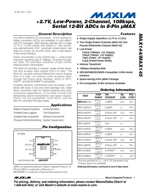
( ) ARE FOR MAX145 ONLY
µMAX/DIP
*Dice are specified at TA = +25°C, DC parameters only. **Contact factory for availability. Ordering Information continued at end of data sheet.
ELECTRICAL CHARACTERISTICS
(V DD = +2.7V to +5.25V, V REF = 2.5V, 0.1µF capacitor at REF, f SCLK = 2.17MHz, 16 clocks/conversion cycle (108ksps), CH- = GND for MAX145, TA = TMIN to TMAX, unless otherwise noted. Typical values are at TA = +25°C.) PARAMETER DC ACCURACY (Note 1) Resolution Relative Accuracy (Note 2) Differential Nonlinearity Offset Error Gain Error Gain Temperature Coefficient Channel-to-Channel Offset Matching Channel-to-Channel Gain Matching (Note 3) ±0.8 ±0.05 ±0.05 RES INL DNL MAX14_A MAX14_B No missing codes over temperature 12 ±0.5 ±1 ±0.75 ±3 ±3 Bits LSB LSB LSB LSB ppm/°C LSB LSB SYMBOL CONDITIONS MIN TYP MAX UNITS
MAX1239MEEE中文资料
Stresses beyond those listed under “Absolute Maximum Ratings” may cause permanent damage to the device. These are stress ratings only, and functional operation of the device at these or any other conditions beyond those indicated in the operational sections of the specifications is not implied. Exposure to absolute maximum rating conditions for extended periods may affect device reliability.
MAX1236–MAX1239
♦ ♦
Applications
Hand-Held Portable Applications Medical Instruments Battery-Powered Test Equipment Solar-Powered Remote Systems Received-Signal-Strength Indicators System Supervision
________________________________________________________________ Maxim Integrated Products
For pricing, delivery, and ordering information, please contact Maxim/Dallas Direct! at 1-888-629-4642, or visit Maxim’s website at .
MAX211ECWI+中文资料

________________________________________________________________Maxim Integrated Products 1General DescriptionThe MAX202E–MAX213E, MAX232E/MAX241E line drivers/receivers are designed for RS-232 and V.28communications in harsh environments. Each transmitter output and receiver input is protected against ±15kV electrostatic discharge (ESD) shocks, without latchup.The various combinations of features are outlined in the Selector Guide.The drivers and receivers for all ten devices meet all EIA/TIA-232E and CCITT V.28specifications at data rates up to 120kbps, when loaded in accordance with the EIA/TIA-232E specification.The MAX211E/MAX213E/MAX241E are available in 28-pin SO packages, as well as a 28-pin SSOP that uses 60% less board space. The MAX202E/MAX232E come in 16-pin TSSOP, narrow SO, wide SO, and DIP packages. The MAX203E comes in a 20-pin DIP/SO package, and needs no external charge-pump capacitors. The MAX205E comes in a 24-pin wide DIP package, and also eliminates external charge-pump capacitors. The MAX206E/MAX207E/MAX208E come in 24-pin SO, SSOP, and narrow DIP packages. The MAX232E/MAX241E operate with four 1µF capacitors,while the MAX202E/MAX206E/MAX207E/MAX208E/MAX211E/MAX213E operate with four 0.1µF capacitors,further reducing cost and board space.________________________ApplicationsNotebook, Subnotebook, and Palmtop Computers Battery-Powered Equipment Hand-Held EquipmentNext-Generation Device Featureso For Low-Voltage ApplicationsMAX3222E/MAX3232E/MAX3237E/MAX3241E/MAX3246E: ±15kV ESD-Protected Down to10nA, +3.0V to +5.5V, Up to 1Mbps, True RS-232Transceivers (MAX3246E Available in a UCSP™Package)o For Low-Power ApplicationsMAX3221/MAX3223/MAX3243: 1µA SupplyCurrent, True +3V to +5.5V RS-232 Transceivers with Auto-Shutdown™o For Space-Constrained ApplicationsMAX3233E/MAX3235E: ±15kV ESD-Protected,1µA, 250kbps, +3.0V/+5.5V, Dual RS-232Transceivers with Internal Capacitorso For Low-Voltage or Data Cable ApplicationsMAX3380E/MAX3381E: +2.35V to +5.5V, 1µA,2Tx/2Rx RS-232 Transceivers with ±15kV ESD-Protected I/O and Logic PinsMAX202E–MAX213E, MAX232E/MAX241E±15kV ESD-Protected, +5V RS-232 TransceiversSelector Guide19-0175; Rev 6; 3/05Pin Configurations and Typical Operating Circuits appear at end of data sheet.YesPARTNO. OF RS-232DRIVERSNO. OF RS-232RECEIVERSRECEIVERS ACTIVE IN SHUTDOWNNO. OF EXTERNAL CAPACITORS(µF)LOW-POWER SHUTDOWNTTL TRI-STATE MAX202E 220 4 (0.1)No No MAX203E 220None No No MAX205E 550None Yes Yes MAX206E 430 4 (0.1)Yes Yes MAX207E 530 4 (0.1)No No MAX208E 440 4 (0.1)No No MAX211E 450 4 (0.1)Yes Yes MAX213E 452 4 (0.1)Yes Yes MAX232E 220 4 (1)No No MAX241E454 (1)YesFor pricing, delivery, and ordering information,please contact Maxim/Dallas Direct!at 1-888-629-4642, or visit Maxim’s website at .AutoShutdown and UCSP are trademarks of Maxim Integrated Products, Inc.Ordering InformationOrdering Information continued at end of data sheet.2_______________________________________________________________________________________M A X 202E –M A X 213E , M A X 232E /M A X 241EABSOLUTE MAXIMUM RATINGSV CC ..........................................................................-0.3V to +6V V+................................................................(V CC - 0.3V) to +14V V-............................................................................-14V to +0.3V Input VoltagesT_IN............................................................-0.3V to (V+ + 0.3V)R_IN...................................................................................±30V Output VoltagesT_OUT.................................................(V- - 0.3V) to (V+ + 0.3V)R_OUT......................................................-0.3V to (V CC + 0.3V)Short-Circuit Duration, T_OUT....................................Continuous Continuous Power Dissipation (T A = +70°C)16-Pin Plastic DIP (derate 10.53mW/°C above +70°C)....842mW 16-Pin Narrow SO (derate 8.70mW/°C above +70°C).....696mW 16-Pin Wide SO (derate 9.52mW/°C above +70°C)......762mW 16-Pin TSSOP (derate 9.4mW/°C above +70°C)...........755mW20-Pin Plastic DIP (derate 11.11mW/°C above +70°C)...889mW 20-Pin SO (derate 10.00mW/°C above +70°C).............800mW 24-Pin Narrow Plastic DIP(derate 13.33mW/°C above +70°C) ...............................1.07W 24-Pin Wide Plastic DIP(derate 14.29mW/°C above +70°C)................................1.14W 24-Pin SO (derate 11.76mW/°C above +70°C).............941mW 24-Pin SSOP (derate 8.00mW/°C above +70°C)..........640mW 28-Pin SO (derate 12.50mW/°C above +70°C)....................1W 28-Pin SSOP (derate 9.52mW/°C above +70°C)..........762mW Operating Temperature RangesMAX2_ _EC_ _.....................................................0°C to +70°C MAX2_ _EE_ _...................................................-40°C to +85°C Storage Temperature Range.............................-65°C to +165°C Lead Temperature (soldering, 10s).................................+300°CELECTRICAL CHARACTERISTICS(V CC = +5V ±10% for MAX202E/206E/208E/211E/213E/232E/241E; V CC = +5V ±5% for MAX203E/205E/207E; C1–C4 = 0.1µF for MAX202E/206E/207E/208E/211E/213E; C1–C4 = 1µF for MAX232E/241E; T A = T MIN to T MAX ; unless otherwise noted. Typical values are at T A = +25°C.)Stresses beyond those listed under “Absolute Maximum Ratings” may cause permanent damage to the device. These are stress ratings only, and functional operation of the device at these or any other conditions beyond those indicated in the operational sections of the specifications is not implied. Exposure to absolute maximum rating conditions for extended periods may affect device reliability.ELECTRICAL CHARACTERISTICS (continued)MAX202E–MAX213E, MAX232E/MAX241E (V CC= +5V ±10% for MAX202E/206E/208E/211E/213E/232E/241E; V CC= +5V ±5% for MAX203E/205E/207E; C1–C4 = 0.1µF forMAX202E/206E/207E/208E/211E/213E; C1–C4 = 1µF for MAX232E/241E; T A= T MIN to T MAX; unless otherwise noted. Typical valuesare at T A= +25°C.)Note 1:MAX211EE_ _ tested with V CC= +5V ±5%._______________________________________________________________________________________34______________________________________________________________________________________M A X 202E –M A X 213E , M A X 232E /M A X 241E__________________________________________Typical Operating Characteristics(Typical Operating Circuits, V CC = +5V, T A = +25°C, unless otherwise noted.)5.00MAX211E/MAX213ETRANSMITTER OUTPUT VOLTAGEvs. LOAD CAPACITANCELOAD CAPACITANCE (pF)V O H , -V O L (V )5.56.06.57.07.58.0100020003000400050000MAX211E/MAX213E/MAX241E TRANSMITTER SLEW RATE vs. LOAD CAPACITANCELOAD CAPACITANCE (pF)S L E W R A T E ( V /µs )5101520253010002000300040005000_______________________________________________________________________________________5MAX202E–MAX213E, MAX232E/MAX241E____________________________Typical Operating Characteristics (continued)(Typical Operating Circuits, V CC = +5V, T A = +25°C, unless otherwise noted.)2MAX202E/MAX203E/MAX232E TRANSMITTER SLEW RATE vs. LOAD CAPACITANCELOAD CAPACITANCE (pF)S L E W R A T E ( V /µs )468101214100020003000400050005.07.5-7.53000MAX205E–MAX208ETRANSMITTER OUTPUT VOLTAGEvs. LOAD CAPACITANCE-5.02.5LOAD CAPACITANCE (pF)O U T P U T V O L T A G E (V )10002000400050000-2.54550203000MAX205E–MAX208E SUPPLY CURRENT vs. LOAD CAPACITANCE2540LOAD CAPACITANCE (pF)S U P P L Y C U R R E N T (m A )100020004000500035302.55.0-10.0180MAX205E –MAX208EOUTPUT VOLTAGE vs. DATA RATE-7.50DATA RATE (kbps)O U T P U T V O L T A G E (V )601202401503090210-2.5-5.010.07.56_______________________________________________________________________________________M A X 202E –M A X 213E , M A X 232E /M A X 241EMAX203EMAX205E_____________________________________________________________Pin DescriptionsMAX202E/MAX232E_______________________________________________________________________________________7MAX202E–MAX213E, MAX232E/MAX241EMAX208E________________________________________________Pin Descriptions (continued)MAX206EMAX207E8_______________________________________________________________________________________M A X 202E –M A X 213E , M A X 232E /M A X 241EMAX211E/MAX213E/MAX241E)(MAX205E/MAX206E/MAX211E/MAX213E/MAX241E)________________________________________________Pin Descriptions (continued)MAX211E/MAX213E/MAX241EFigure 3. Transition Slew-Rate Circuit_______________Detailed Description The MAX202E–MAX213E, MAX232E/MAX241E consist of three sections: charge-pump voltage converters, drivers (transmitters), and receivers. These E versions provide extra protection against ESD. They survive ±15kV discharges to the RS-232 inputs and outputs, tested using the Human Body Model. When tested according to IEC1000-4-2, they survive ±8kV contact-discharges and ±15kV air-gap discharges. The rugged E versions are intended for use in harsh environments or applications where the RS-232 connection is frequently changed (such as notebook computers). The standard (non-“E”) MAX202, MAX203, MAX205–MAX208, MAX211, MAX213, MAX232, and MAX241 are recommended for applications where cost is critical.+5V to ±10V Dual Charge-PumpVoltage Converter The +5V to ±10V conversion is performed by dual charge-pump voltage converters (Figure 4). The first charge-pump converter uses capacitor C1 to double the +5V into +10V, storing the +10V on the output filter capacitor, C3. The second uses C2 to invert the +10V into -10V, storing the -10V on the V- output filter capacitor, C4.In shutdown mode, V+ is internally connected to V CC by a 1kΩpull-down resistor, and V- is internally connected to ground by a 1kΩpull up resistor.RS-232 Drivers With V CC= 5V, the typical driver output voltage swing is ±8V when loaded with a nominal 5kΩRS-232 receiver. The output swing is guaranteed to meet EIA/TIA-232E and V.28 specifications that call for ±5V minimum output levels under worst-case conditions. These include a 3kΩload, minimum V CC, and maximum operating temperature. The open-circuit output voltage swings from (V+ - 0.6V) to V-.Input thresholds are CMOS/TTL compatible. The unused drivers’ inputs on the MAX205E–MAX208E, MAX211E, MAX213E, and MAX241E can be left unconnected because 400kΩpull up resistors to V CC are included on-chip. Since all drivers invert, the pull up resistors force the unused drivers’ outputs low. The MAX202E, MAX203E, and MAX232E do not have pull up resistors on the transmitter inputs._______________________________________________________________________________________9MAX202E–MAX213E, MAX232E/MAX241E10______________________________________________________________________________________M A X 202E –M A X 213E , M A X 232E /M A X 241E±15kV ESD-Protected, +5V RS-232 Transceivers When in low-power shutdown mode, the MAX205E/MAX206E/MAX211E/MAX213E/MAX241E driver outputs are turned off and draw only leakage currents—even if they are back-driven with voltages between 0V and 12V. Below -0.5V in shutdown, the transmitter output is diode-clamped to ground with a 1k Ωseries impedance.RS-232 ReceiversThe receivers convert the RS-232 signals to CMOS-logic output levels. The guaranteed 0.8V and 2.4V receiver input thresholds are significantly tighter than the ±3V thresholds required by the EIA/TIA-232E specification.This allows the receiver inputs to respond to TTL/CMOS-logic levels, as well as RS-232 levels.The guaranteed 0.8V input low threshold ensures that receivers shorted to ground have a logic 1 output. The 5k Ωinput resistance to ground ensures that a receiver with its input left open will also have a logic 1 output. Receiver inputs have approximately 0.5V hysteresis.This provides clean output transitions, even with slow rise/fall-time signals with moderate amounts of noise and ringing.In shutdown, the MAX213E’s R4 and R5 receivers have no hysteresis.Shutdown and Enable Control (MAX205E/MAX206E/MAX211E/MAX213E/MAX241E)In shutdown mode, the charge pumps are turned off,V+ is pulled down to V CC , V- is pulled to ground, and the transmitter outputs are disabled. This reduces supply current typically to 1µA (15µA for the MAX213E).The time required to exit shutdown is under 1ms, as shown in Figure 5.ReceiversAll MAX213E receivers, except R4 and R5, are put into a high-impedance state in shutdown mode (see Tables 1a and 1b). The MAX213E’s R4 and R5 receivers still function in shutdown mode. These two awake-in-shutdown receivers can monitor external activity while maintaining minimal power consumption.The enable control is used to put the receiver outputs into a high-impedance state, to allow wire-OR connection of two EIA/TIA-232E ports (or ports of different types) at the UART. It has no effect on the RS-232 drivers or the charge pumps.N ote: The enabl e control pin is active l ow for the MAX211E/MAX241E (EN ), but is active high for the MAX213E (EN). The shutdown control pin is active high for the MAX205E/MAX206E/MAX211E/MAX241E (SHDN), but is active low for the MAX213E (SHDN ).Figure 4. Charge-Pump DiagramMAX202E–MAX213E, MAX232E/MAX241EV+V-200µs/div3V 0V 10V 5V 0V -5V -10VSHDNMAX211EFigure 5. MAX211E V+ and V- when Exiting Shutdown (0.1µF capacitors)X = Don't care.*Active = active with reduced performanceSHDN E N OPERATION STATUS Tx Rx 00Normal Operation All Active All Active 01Normal Operation All Active All High-Z 1XShutdownAll High-ZAll High-ZTable 1a. MAX205E/MAX206E/MAX211E/MAX241E Control Pin ConfigurationsTable 1b. MAX213E Control Pin ConfigurationsThe MAX213E’s receiver propagation delay is typically 0.5µs in normal operation. In shutdown mode,propagation delay increases to 4µs for both rising and falling transitions. The MAX213E’s receiver inputs have approximately 0.5V hysteresis, except in shutdown,when receivers R4 and R5 have no hysteresis.When entering shutdown with receivers active, R4 and R5 are not valid until 80µs after SHDN is driven low.When coming out of shutdown, all receiver outputs are invalid until the charge pumps reach nominal voltage levels (less than 2ms when using 0.1µF capacitors).±15kV ESD ProtectionAs with all Maxim devices, ESD-protection structures are incorporated on all pins to protect against electrostatic discharges encountered during handling and assembly. The driver outputs and receiver inputs have extra protection against static electricity. Maxim’s engineers developed state-of-the-art structures to protect these pins against ESD of ±15kV without damage. The ESD structures withstand high ESD in all states: normal operation, shutdown, and powered down. After an ESD event, Maxim’s E versions keep working without latchup, whereas competing RS-232products can latch and must be powered down to remove latchup.ESD protection can be tested in various ways; the transmitter outputs and receiver inputs of this product family are characterized for protection to the following limits:1)±15kV using the Human Body Model2)±8kV using the contact-discharge method specifiedin IEC1000-4-23)±15kV using IEC1000-4-2’s air-gap method.ESD Test ConditionsESD performance depends on a variety of conditions.Contact Maxim for a reliability report that documents test set-up, test methodology, and test results.Human Body ModelFigure 6a shows the Human Body Model, and Figure 6b shows the current waveform it generates when discharged into a low impedance. This model consists of a 100pF capacitor charged to the ESD voltage of interest, which is then discharged into the test device through a 1.5k Ωresistor.S H D N ENOPERATION STATUS Tx 1–400Shutdown All High-Z 01Shutdown All High-Z 10Normal Operation 11Normal OperationAll ActiveAll Active Active1–34, 5High-Z ActiveHigh-Z High-Z High-Z Active*High-Z RxM A X 202E –M A X 213E , M A X 232E /M A X 241EIEC1000-4-2The IEC1000-4-2 standard covers ESD testing and performance of finished equipment; it does not specifically refer to integrated circuits. The MAX202E/MAX203E–MAX213E, MAX232E/MAX241E help you design equipment that meets level 4 (the highest level) of IEC1000-4-2, without the need for additional ESD-protection components.The major difference between tests done using the Human Body Model and IEC1000-4-2 is higher peak current in IEC1000-4-2, because series resistance is lower in the IEC1000-4-2 model. Hence, the ESD withstand voltage measured to IEC1000-4-2 is generally lower than that measured using the Human Body Model. Figure 7b shows the current waveform for the 8kV IEC1000-4-2 level-four ESD contact-discharge test.The air-gap test involves approaching the device with a charged probe. The contact-discharge method connects the probe to the device before the probe is energized.Machine ModelThe Machine Model for ESD tests all pins using a 200pF storage capacitor and zero discharge resistance. Its objective is to emulate the stress caused by contact that occurs with handling and assembly during manufacturing. Of course, all pins require this protection during manufacturing, not just RS-232 inputs and outputs. Therefore,after PC board assembly,theMachine Model is less relevant to I/O ports.Figure 7a. IEC1000-4-2 ESD Test ModelFigure 7b. IEC1000-4-2 ESD Generator Current WaveformFigure 6a. Human Body ESD Test ModelFigure 6b. Human Body Model Current Waveform__________Applications InformationCapacitor Selection The capacitor type used for C1–C4 is not critical for proper operation. The MAX202E, MAX206–MAX208E, MAX211E, and MAX213E require 0.1µF capacitors, and the MAX232E and MAX241E require 1µF capacitors, although in all cases capacitors up to 10µF can be used without harm. Ceramic, aluminum-electrolytic, or tantalum capacitors are suggested for the 1µF capacitors, and ceramic dielectrics are suggested for the 0.1µF capacitors. When using the minimum recommended capacitor values, make sure the capacitance value does not degrade excessively as the operating temperature varies. If in doubt, use capacitors with a larger (e.g., 2x) nominal value. The capacitors’ effective series resistance (ESR), which usually rises at low temperatures, influences the amount of ripple on V+ and V-.Use larger capacitors (up to 10µF) to reduce the output impedance at V+ and V-. This can be useful when “stealing” power from V+ or from V-. The MAX203E and MAX205E have internal charge-pump capacitors. Bypass V CC to ground with at least 0.1µF. In applications sensitive to power-supply noise generated by the charge pumps, decouple V CC to ground with a capacitor the same size as (or larger than) the charge-pump capacitors (C1–C4).V+ and V- as Power Supplies A small amount of power can be drawn from V+ and V-, although this will reduce both driver output swing and noise margins. Increasing the value of the charge-pump capacitors (up to 10µF) helps maintain performance when power is drawn from V+ or V-.Driving Multiple Receivers Each transmitter is designed to drive a single receiver. Transmitters can be paralleled to drive multiple receivers.Driver Outputs when Exiting Shutdown The driver outputs display no ringing or undesirable transients as they come out of shutdown.High Data Rates These transceivers maintain the RS-232 ±5.0V minimum driver output voltages at data rates of over 120kbps. For data rates above 120kbps, refer to the Transmitter Output Voltage vs. Load Capacitance graphs in the Typical Operating Characteristics. Communication at these high rates is easier if the capacitive loads on the transmitters are small; i.e., short cables are best.Table 2. Summary of EIA/TIA-232E, V.28 SpecificationsMAX202E–MAX213E, MAX232E/MAX241EM A X 202E –M A X 213E , M A X 232E /M A X 241E____________Pin Configurations and Typical Operating Circuits (continued)Table 3. DB9 Cable ConnectionsCommonly Used for EIA/TIAE-232E and V.24 Asynchronous Interfaces____________Pin Configurations and Typical Operating Circuits (continued)MAX202E–MAX213E, MAX232E/MAX241EM A X 202E –M A X 213E , M A X 232E /M A X 241E____________Pin Configurations and Typical Operating Circuits (continued)MAX202E–MAX213E, MAX232E/MAX241E____________Pin Configurations and Typical Operating Circuits (continued)M A X 202E –M A X 213E , M A X 232E /M A X 241E____________Pin Configurations and Typical Operating Circuits (continued)MAX202E–MAX213E, MAX232E/MAX241E____________Pin Configurations and Typical Operating Circuits (continued)M A X 202E –M A X 213E , M A X 232E /M A X 241E____________Pin Configurations and Typical Operating Circuits (continued)______________________________________________________________________________________21MAX202E–MAX213E, MAX232E/MAX241E Ordering Information (continued)*Dice are specified at T A= +25°C.M A X 202E –M A X 213E , M A X 232E /M A X 241E22________________________________________________________________________________________________________________________________________________Chip Topographies___________________Chip InformationC1-V+C1+V CC R2INT2OUT R2OUT0.117"(2.972mm)0.080"(2.032mm)V-C2+ C2-T2IN T1OUT R1INR1OUT T1INGNDR5INV-C2-C2+C1-V+C1+V CC T4OUTR3IN T3OUTT1OUT 0.174"(4.420mm)0.188"(4.775mm)T4IN R5OUT R4OUT T3IN R4IN EN (EN) SHDN (SHDN)R3OUT T2OUT GNDR1IN R1OUT T2IN R2OUTR2IN T1IN ( ) ARE FOR MAX213E ONLYTRANSISTOR COUNT: 123SUBSTRATE CONNECTED TO GNDTRANSISTOR COUNT: 542SUBSTRATE CONNECTED TO GNDMAX202E/MAX232EMAX211E/MAX213E/MAX241EMAX205E/MAX206E/MAX207E/MAX208E TRANSISTOR COUNT: 328SUBSTRATE CONNECTED TO GNDMAX202E–MAX213E, MAX232E/MAX241E Package InformationM A X 202E –M A X 213E , M A X 232E /M A X 241EPackage Information (continued)MAX202E–MAX213E, MAX232E/MAX241E±15kV ESD-Protected, +5V RS-232 TransceiversMaxim cannot assume responsibility for use of any circuitry other than circuitry entirely embodied in a Maxim product. No circuit patent licenses are implied. Maxim reserves the right to change the circuitry and specifications without notice at any time.Maxim Integrated Products, 120 San Gabriel Drive, Sunnyvale, CA 94086 408-737-7600 ____________________25©2005 Maxim Integrated ProductsPrinted USAis a registered trademark of Maxim Integrated Products, Inc.Package Information (continued)(The package drawing(s) in this data sheet may not reflect the most current specifications. For the latest package outline information go to /packages .)。
MAX2605-MAX2609中文资料
General DescriptionThe MAX2605–MAX2609 evaluation kits (EV kits) simplify evaluation of this family of voltage-controlled oscillators (VCOs). These kits enable testing of the devices’ per-formance and require no additional support circuitry.Both signal outputs use SMA connectors to facilitate connection to RF test equipment.These EV kits are fully assembled and tested. Their oscil-lation frequencies are set to approximately the midrange of the respective VCOs.Featureso Easy Evaluationo Complete, Tunable VCO Test Board with Tank Circuit o Low Phase Noiseo Fully Assembled and TestedEvaluate: MAX2605–MAX2609MAX2605–MAX2609 Evaluation Kits19-1673 Rev 0; 9/00Ordering InformationComponent SuppliersFor free samples and the latest literature, visit or phone 1-800-998-8800.For small orders, phone 1-800-835-8769.MAX2606 Component ListMAX2605 Component ListE v a l u a t e : M A X 2605–M A X 2609MAX2605–MAX2609 Evaluation Kits 2_______________________________________________________________________________________Quick StartThe MAX2605–MAX2609 evaluation kits are fully assembled and factory tested. Follow the instructions in the Connections a nd Setup section for proper device evaluation.Test Equipment Required•Low-noise power supplies (these are recommended for oscillator noise measurement). Noise or ripple will frequency-modulate the oscillator and cause spectral spreading. Batteries can be used in place of power supplies, if necessary.– Use a DC power supply capable of supplying +2.7V to +5.5V. Alternatively, use two or three 1.5V batteries.– Use a DC power supply capable of supplying +0.4V to +2.4V, continuously variable, for TUNE.Alternatively, use two 1.5V batteries with a resistive voltage divider or potentiometer.•An RF spectrum analyzer that covers the operating frequency range of the MAX2605–MAX2609• A 50Ωcoaxial cable with SMA connectors •An ammeter (optional)Connections and Setup1)Connect a DC supply (preset to +3V) to the V CC and GND terminals (through an ammeter, if desired) on the EV kit.2)Turn on the DC supply. If used, the ammeter readingMAX2607 Component ListMAX2608 Component ListEvaluate: MAX2605–MAX2609MAX2605–MAX2609 Evaluation Kits_______________________________________________________________________________________3approximates the typical operating current specified in the MAX2605–MAX2609 data sheet.3)Connect the VCO output (OUT+ or OUT-) to a spec-trum analyzer with a 50Ωcoaxial cable.4)Apply a positive variable DC voltage between 0.4V and 2.4V to TUNE.5)Check the tuning bandwidth on the spectrum analyz-er by varying the tuning voltage (+0.4V to +2.4V).Layout ConsiderationsThe EV kit PC board can serve as a guide for laying out a board using the MAX2605–MAX2609. Generally, the VCC pin on the PC board should have a decoupling capacitor placed close to the IC. This minimizes noisecoupling from the supply. Also, place the VCO as far away as possible from the noisy section of a larger sys-tem, such as a switching regulator or digital circuits.The VCO ’s performance is strongly dependent on the availability of the external tuning inductor. For best per-formance, use high-Q components and choose their val-ues carefully. To minimize the effects of parasitic ele-ments, which degrade circuit performance, place the tuning inductor and C BYP close to the VCO. For higher-frequency versions, include the parasitic PC board inductance and capacitance when calculating the oscillation frequency. In addition, remove the ground plane around and under the tuning inductor to minimize the effect of parasitic capacitance.Noise on TUNE translates into FM noise on the outputs;therefore, keep the trace between TUNE and the control circuitry as short as possible. If necessary, use an RC filter to further suppress noise, as done on the EV kits.E v a l u a t e : M A X 2605–M A X 2609MAX2605–MAX2609 Evaluation Kits 4_______________________________________________________________________________________Figure 2. MAX2608/MAX2609 EV Kits SchematicFigure 1. MAX2605/MAX2606/MAX2607 EV Kits SchematicEvaluate: MAX2605–MAX2609MAX2605–MAX2609 Evaluation Kits_______________________________________________________________________________________5Figure 3. MAX2605/MAX2606/MAX2607 EV Kits ComponentPlacement Guide—Top Silk ScreenFigure 4. MAX2608/MAX2609 EV Kits Component PlacementGuide—Top Silk ScreenFigure 5. MAX2605/MAX2606/MAX2607 EV Kits PC BoardLayout—Component SideFigure 6. MAX2608/MAX2609 EV Kits PC Board Layout—Component SideMa xim ca nnot a ssume responsibility for use of a ny circuitry other tha n circuitry entirely embodied in a Ma xim product. No circuit pa tent licenses a re implied. Maxim reserves the right to change the circuitry and specifications without notice at any time.6_____________________Maxim Integrated Products, 120 San Gabriel Drive, Sunnyvale, CA 94086 408-737-7600©2000 Maxim Integrated ProductsPrinted USAis a registered trademark of Maxim Integrated Products.E v a l u a t e : M A X 2605–M A X 2609MAX2605–MAX2609 Evaluation Kits Figure 7. MAX2605/MAX2606/MAX2607/MAX2608/MAX2609EV Kits PC Board Layout—Ground Plane。
MAX691AEWE中文资料
ELECTRICAL CHARACTERISTICS
(MAX691A, MAX800L: VCC = +4.75V to +5.5V, MAX693A, MAX800M: VCC = +4.5V to +5.5V, VBATT = 2.8V, TA = TMIN to TMAX, unless otherwise noted.)
BATT ON 5 LOW LINE 6
OSC IN 7 OSC SEL 8
MAX691A MAX693A MAX800L MAX800M
16 RESET 15 RESET 14 WDO 13 CE IN 12 CE OUT 11 WDI 10 PFO 9 PFI
DIP/SO
SuperCap is a registered trademark of Baknor Industries. MaxCap is a registered trademark of The Carborundum Corp.
元器件交易网
19-0094; Rev 7a; 12/96
Microprocessor Supervisory Circuits
MAX691A/MAX693A/MAX800L/MAX800M
_______________General Description
The MAX691A/MAX693A/MAX800L/MAX800M microprocessor (µP) supervisory circuits are pin-compatible upgrades to the MAX691, MAX693, and MAX695. They improve performance with 30µA supply current, 200ms typ reset active delay on power-up, and 6ns chipenable propagation delay. Features include write protection of CMOS RAM or EEPROM, separate watchdog outputs, backup-battery switchover, and a RESET output that is valid with VCC down to 1V. The MAX691A/ MAX800L have a 4.65V typical reset-threshold voltage, and the MAX693A/MAX800M’s reset threshold is 4.4V typical. The MAX800L/MAX800M guarantee power-fail accuracies to ±2%.
MAX2681中文资料
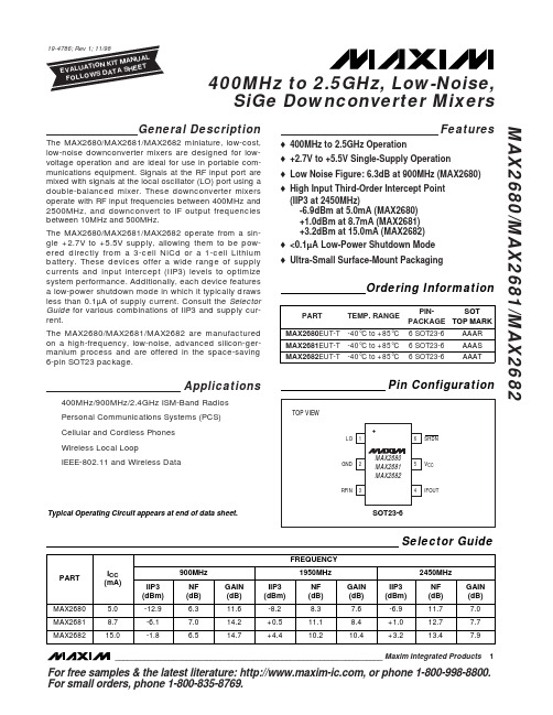
MAX2680
5.0
MAX2681
8.7
MAX2682
15.0
IIP3 (dBm)
-12.9 -6.1 -1.8
900MHz NF (dB) 6.3 7.0 6.5
GAIN (dB)
11.6 14.2 14.7
FREQUENCY 1950MHz
IIP3 (dBm)
NF (dB)
GAIN (dB)
-8.2
Features
o 400MHz to 2.5GHz Operation
o +2.7V to +5.5V Single-Supply Operation
o Low Noise Figure: 6.3dB at 900MHz (MAX2680)
o High Input Third-Order Intercept Point (IIP3 at 2450MHz) -6.9dBm at 5.0mA (MAX2680) +1.0dBm at 8.7mA (MAX2681) +3.2dBm at 15.0mA (MAX2682)
MAX2681EUT-T -40°C to +85°C 6 SOT23-6 MAX2682EUT-T -40°C to +85°C 6 SOT23-6
AAAS AAAT
Applications
400MHz/900MHz/2.4GHz ISM-Band Radios Personal Communications Systems (PCS) Cellular and Cordless Phones Wireless Local Loop IEEE-802.11 and Wireless Data