CD40103BEE4中文资料
CD4045BEE4中文资料
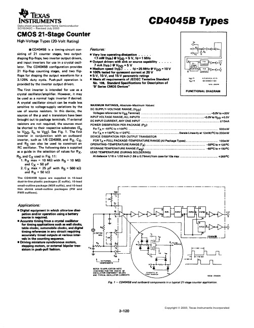
The CD4045B types are supplied in 16-lead dual-in-line plastic packages (E suffix), 16-lead small-outline package (NSR suffix), and 16-lead thin shrink small-outline packages (PW and PWR suffixes).PACKAGING INFORMATIONOrderable Device Status(1)PackageType PackageDrawingPins PackageQtyEco Plan(2)Lead/Ball Finish MSL Peak Temp(3)CD4045BE ACTIVE PDIP N1625Pb-Free(RoHS)CU NIPDAU N/A for Pkg TypeCD4045BEE4ACTIVE PDIP N1625Pb-Free(RoHS)CU NIPDAU N/A for Pkg TypeCD4045BNSR ACTIVE SO NS162000Green(RoHS&no Sb/Br)CU NIPDAU Level-1-260C-UNLIMCD4045BNSRE4ACTIVE SO NS162000Green(RoHS&no Sb/Br)CU NIPDAU Level-1-260C-UNLIMCD4045BNSRG4ACTIVE SO NS162000Green(RoHS&no Sb/Br)CU NIPDAU Level-1-260C-UNLIMCD4045BPW ACTIVE TSSOP PW1690Green(RoHS&no Sb/Br)CU NIPDAU Level-1-260C-UNLIMCD4045BPWE4ACTIVE TSSOP PW1690Green(RoHS&no Sb/Br)CU NIPDAU Level-1-260C-UNLIMCD4045BPWG4ACTIVE TSSOP PW1690Green(RoHS&no Sb/Br)CU NIPDAU Level-1-260C-UNLIMCD4045BPWR ACTIVE TSSOP PW162000Green(RoHS&no Sb/Br)CU NIPDAU Level-1-260C-UNLIMCD4045BPWRE4ACTIVE TSSOP PW162000Green(RoHS&no Sb/Br)CU NIPDAU Level-1-260C-UNLIMCD4045BPWRG4ACTIVE TSSOP PW162000Green(RoHS&no Sb/Br)CU NIPDAU Level-1-260C-UNLIM(1)The marketing status values are defined as follows:ACTIVE:Product device recommended for new designs.LIFEBUY:TI has announced that the device will be discontinued,and a lifetime-buy period is in effect.NRND:Not recommended for new designs.Device is in production to support existing customers,but TI does not recommend using this part in a new design.PREVIEW:Device has been announced but is not in production.Samples may or may not be available.OBSOLETE:TI has discontinued the production of the device.(2)Eco Plan-The planned eco-friendly classification:Pb-Free(RoHS),Pb-Free(RoHS Exempt),or Green(RoHS&no Sb/Br)-please check /productcontent for the latest availability information and additional product content details.TBD:The Pb-Free/Green conversion plan has not been defined.Pb-Free(RoHS):TI's terms"Lead-Free"or"Pb-Free"mean semiconductor products that are compatible with the current RoHS requirements for all6substances,including the requirement that lead not exceed0.1%by weight in homogeneous materials.Where designed to be soldered at high temperatures,TI Pb-Free products are suitable for use in specified lead-free processes.Pb-Free(RoHS Exempt):This component has a RoHS exemption for either1)lead-based flip-chip solder bumps used between the die and package,or2)lead-based die adhesive used between the die and leadframe.The component is otherwise considered Pb-Free(RoHS compatible)as defined above.Green(RoHS&no Sb/Br):TI defines"Green"to mean Pb-Free(RoHS compatible),and free of Bromine(Br)and Antimony(Sb)based flame retardants(Br or Sb do not exceed0.1%by weight in homogeneous material)(3)MSL,Peak Temp.--The Moisture Sensitivity Level rating according to the JEDEC industry standard classifications,and peak solder temperature.Important Information and Disclaimer:The information provided on this page represents TI's knowledge and belief as of the date that it is provided.TI bases its knowledge and belief on information provided by third parties,and makes no representation or warranty as to the accuracy of such information.Efforts are underway to better integrate information from third parties.TI has taken and continues to take reasonable steps to provide representative and accurate information but may not have conducted destructive testing or chemical analysis on incoming materials and chemicals.TI and TI suppliers consider certain information to be proprietary,and thus CAS numbers and other limited information may not be available for release.In no event shall TI's liability arising out of such information exceed the total purchase price of the TI part(s)at issue in this document sold by TIto Customer on an annual basis.TAPE AND REEL INFORMATION*All dimensions are nominalDevicePackage Type Package Drawing Pins SPQReel Diameter (mm)Reel Width W1(mm)A0(mm)B0(mm)K0(mm)P1(mm)W (mm)Pin1Quadrant CD4045BNSR SO NS 162000330.016.48.210.5 2.512.016.0Q1CD4045BPWRTSSOPPW162000330.012.47.05.61.68.012.0Q1*All dimensions are nominalDevice Package Type Package Drawing Pins SPQ Length(mm)Width(mm)Height(mm) CD4045BNSR SO NS162000346.0346.033.0 CD4045BPWR TSSOP PW162000346.0346.029.0IMPORTANT NOTICETexas Instruments Incorporated and its subsidiaries(TI)reserve the right to make corrections,modifications,enhancements,improvements, and other changes to its products and services at any time and to discontinue any product or service without notice.Customers should obtain the latest relevant information before placing orders and should verify that such information is current and complete.All products are sold subject to TI’s terms and conditions of sale supplied at the time of order acknowledgment.TI warrants performance of its hardware products to the specifications applicable at the time of sale in accordance with TI’s standard warranty.Testing and other quality control techniques are used to the extent TI deems necessary to support this warranty.Except where mandated by government requirements,testing of all parameters of each product is not necessarily performed.TI assumes no liability for applications assistance or customer product design.Customers are responsible for their products and applications using TI components.To minimize the risks associated with customer products and applications,customers should provide adequate design and operating safeguards.TI does not warrant or represent that any license,either express or implied,is granted under any TI patent right,copyright,mask work right, or other TI intellectual property right relating to any combination,machine,or process in which TI products or services are rmation published by TI regarding third-party products or services does not constitute a license from TI to use such products or services or a warranty or endorsement e of such information may require a license from a third party under the patents or other intellectual property of the third party,or a license from TI under the patents or other intellectual property of TI.Reproduction of TI information in TI data books or data sheets is permissible only if reproduction is without alteration and is accompanied by all associated warranties,conditions,limitations,and notices.Reproduction of this information with alteration is an unfair and deceptive business practice.TI is not responsible or liable for such altered rmation of third parties may be subject to additional restrictions.Resale of TI products or services with statements different from or beyond the parameters stated by TI for that product or service voids all express and any implied warranties for the associated TI product or service and is an unfair and deceptive business practice.TI is not responsible or liable for any such statements.TI products are not authorized for use in safety-critical applications(such as life support)where a failure of the TI product would reasonably be expected to cause severe personal injury or death,unless officers of the parties have executed an agreement specifically governing such use.Buyers represent that they have all necessary expertise in the safety and regulatory ramifications of their applications,and acknowledge and agree that they are solely responsible for all legal,regulatory and safety-related requirements concerning their products and any use of TI products in such safety-critical applications,notwithstanding any applications-related information or support that may be provided by TI.Further,Buyers must fully indemnify TI and its representatives against any damages arising out of the use of TI products in such safety-critical applications.TI products are neither designed nor intended for use in military/aerospace applications or environments unless the TI products are specifically designated by TI as military-grade or"enhanced plastic."Only products designated by TI as military-grade meet military specifications.Buyers acknowledge and agree that any such use of TI products which TI has not designated as military-grade is solely at the Buyer's risk,and that they are solely responsible for compliance with all legal and regulatory requirements in connection with such use. TI products are neither designed nor intended for use in automotive applications or environments unless the specific TI products are designated by TI as compliant with ISO/TS16949requirements.Buyers acknowledge and agree that,if they use any non-designated products in automotive applications,TI will not be responsible for any failure to meet such requirements.Following are URLs where you can obtain information on other Texas Instruments products and application solutions:Products ApplicationsAmplifiers AudioData Converters AutomotiveDSP BroadbandClocks and Timers Digital ControlInterface MedicalLogic MilitaryPower Mgmt Optical NetworkingMicrocontrollers SecurityRFID TelephonyRF/IF and ZigBee®Solutions Video&ImagingWirelessMailing Address:Texas Instruments,Post Office Box655303,Dallas,Texas75265Copyright©2008,Texas Instruments Incorporated。
三态RS锁存触发器CD4043中文资料(引脚图,真值表及电气参数)
三态RS锁存触发器CD4043中文资料(引脚图,真值表及电气参数)
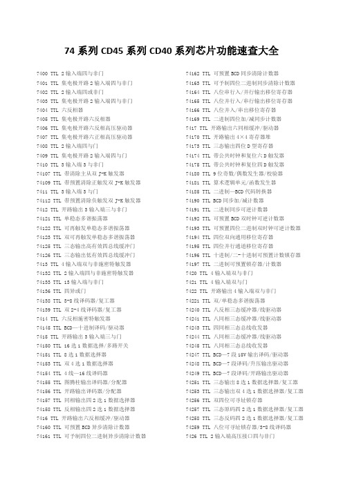
CD4043:四三态R-S锁存触发器(高电平触发)当EN为逻辑1或高电平时,Q端输岀内部锁存器的状态;当EN逻辑0或低电平时,Q端呈高阻抗状态。
CD4043为四交叉耦合三态COS/MOS或非锁存器,具有独立Q输岀端和单独的置位S和复位R输入端。
Q输岀有三态功能,由公共的三态控制输入端EN控制。
三态功能使CD4043输岀可以直接
连到系统总线上。
CD4043真值表:
CD4043引脚图:
CD4043引脚功能图
CD4043引脚功能描述
CD4043内部结构图:
CD4043方框图
CD4043电气参数:
Recomme nded Operati ng Con diti ons 建议操作条件:
CD4044中文资料。
74系列CD45系列CD40系列芯片功能速查大全
74系列CD45系列CD40系列芯片功能速查大全7400 TTL 2输入端四与非门7401 TTL 集电极开路2输入端四与非门7402 TTL 2输入端四或非门7403 TTL 集电极开路2输入端四与非门7404 TTL 六反相器7405 TTL 集电极开路六反相器7406 TTL 集电极开路六反相高压驱动器7407 TTL 集电极开路六正相高压驱动器7408 TTL 2输入端四与门7409 TTL 集电极开路2输入端四与门7410 TTL 3输入端3与非门74107 TTL 带清除主从双J-K触发器74109 TTL 带预置清除正触发双J-K触发器7411 TTL 3输入端3与门74112 TTL 带预置清除负触发双J-K触发器7412 TTL 开路输出3输入端三与非门74121 TTL 单稳态多谐振荡器74122 TTL 可再触发单稳态多谐振荡器74123 TTL 双可再触发单稳态多谐振荡器74125 TTL 三态输出高有效四总线缓冲门74126 TTL 三态输出低有效四总线缓冲门7413 TTL 4输入端双与非施密特触发器74132 TTL 2输入端四与非施密特触发器74133 TTL 13输入端与非门74136 TTL 四异或门74138 TTL 3-8线译码器/复工器74139 TTL 双2-4线译码器/复工器7414 TTL 六反相施密特触发器74145 TTL BCD—十进制译码/驱动器7415 TTL 开路输出3输入端三与门74150 TTL 16选1数据选择/多路开关74151 TTL 8选1数据选择器74153 TTL 双4选1数据选择器74154 TTL 4线—16线译码器74155 TTL 图腾柱输出译码器/分配器74156 TTL 开路输出译码器/分配器74157 TTL 同相输出四2选1数据选择器74158 TTL 反相输出四2选1数据选择器7416 TTL 开路输出六反相缓冲/驱动器74160 TTL 可预置BCD异步清除计数器74161 TTL 可予制四位二进制异步清除计数器74162 TTL 可预置BCD同步清除计数器74163 TTL 可予制四位二进制同步清除计数器74164 TTL 八位串行入/并行输出移位寄存器74165 TTL 八位并行入/串行输出移位寄存器74166 TTL 八位并入/串出移位寄存器74169 TTL 二进制四位加/减同步计数器7417 TTL 开路输出六同相缓冲/驱动器74170 TTL 开路输出4×4寄存器堆74173 TTL 三态输出四位D型寄存器74174 TTL 带公共时钟和复位六D触发器74175 TTL 带公共时钟和复位四D触发器74180 TTL 9位奇数/偶数发生器/校验器74181 TTL 算术逻辑单元/函数发生器74185 TTL 二进制—BCD代码转换器74190 TTL BCD同步加/减计数器74191 TTL 二进制同步可逆计数器74192 TTL 可预置BCD双时钟可逆计数器74193 TTL 可预置四位二进制双时钟可逆计数器74194 TTL 四位双向通用移位寄存器74195 TTL 四位并行通道移位寄存器74196 TTL 十进制/二-十进制可预置计数锁存器74197 TTL 二进制可预置锁存器/计数器7420 TTL 4输入端双与非门7421 TTL 4输入端双与门7422 TTL 开路输出4输入端双与非门74221 TTL 双/单稳态多谐振荡器74240 TTL 八反相三态缓冲器/线驱动器74241 TTL 八同相三态缓冲器/线驱动器74243 TTL 四同相三态总线收发器74244 TTL 八同相三态缓冲器/线驱动器74245 TTL 八同相三态总线收发器74247 TTL BCD—7段15V输出译码/驱动器74248 TTL BCD—7段译码/升压输出驱动器74249 TTL BCD—7段译码/开路输出驱动器74251 TTL 三态输出8选1数据选择器/复工器74253 TTL 三态输出双4选1数据选择器/复工器74256 TTL 双四位可寻址锁存器74257 TTL 三态原码四2选1数据选择器/复工器74258 TTL 三态反码四2选1数据选择器/复工器74259 TTL 八位可寻址锁存器/3-8线译码器7426 TTL 2输入端高压接口四与非门74260 TTL 5输入端双或非门74266 TTL 2输入端四异或非门7427 TTL 3输入端三或非门74273 TTL 带公共时钟复位八D触发器74279 TTL 四图腾柱输出S-R锁存器7428 TTL 2输入端四或非门缓冲器74283 TTL 4位二进制全加器74290 TTL 二/五分频十进制计数器74293 TTL 二/八分频四位二进制计数器74295 TTL 四位双向通用移位寄存器74298 TTL 四2输入多路带存贮开关74299 TTL 三态输出八位通用移位寄存器7430 TTL 8输入端与非门7432 TTL 2输入端四或门74322 TTL 带符号扩展端八位移位寄存器74323 TTL 三态输出八位双向移位/存贮寄存器7433 TTL 开路输出2输入端四或非缓冲器74347 TTL BCD—7段译码器/驱动器74352 TTL 双4选1数据选择器/复工器74353 TTL 三态输出双4选1数据选择器/复工器74365 TTL 门使能输入三态输出六同相线驱动器74365 TTL 门使能输入三态输出六同相线驱动器74366 TTL 门使能输入三态输出六反相线驱动器74367 TTL 4/2线使能输入三态六同相线驱动器74368 TTL 4/2线使能输入三态六反相线驱动器7437 TTL 开路输出2输入端四与非缓冲器74373 TTL 三态同相八D锁存器74374 TTL 三态反相八D锁存器74375 TTL 4位双稳态锁存器74377 TTL 单边输出公共使能八D锁存器74378 TTL 单边输出公共使能六D锁存器74379 TTL 双边输出公共使能四D锁存器7438 TTL 开路输出2输入端四与非缓冲器74380 TTL 多功能八进制寄存器7439 TTL 开路输出2输入端四与非缓冲器74390 TTL 双十进制计数器74393 TTL 双四位二进制计数器7440 TTL 4输入端双与非缓冲器7442 TTL BCD—十进制代码转换器74352 TTL 双4选1数据选择器/复工器74353 TTL 三态输出双4选1数据选择器/复工器74365 TTL 门使能输入三态输出六同相线驱动器74366 TTL 门使能输入三态输出六反相线驱动器74367 TTL 4/2线使能输入三态六同相线驱动器74368 TTL 4/2线使能输入三态六反相线驱动器7437 TTL 开路输出2输入端四与非缓冲器74373 TTL 三态同相八D锁存器74374 TTL 三态反相八D锁存器74375 TTL 4位双稳态锁存器74377 TTL 单边输出公共使能八D锁存器74378 TTL 单边输出公共使能六D锁存器74379 TTL 双边输出公共使能四D锁存器7438 TTL 开路输出2输入端四与非缓冲器74380 TTL 多功能八进制寄存器7439 TTL 开路输出2输入端四与非缓冲器74390 TTL 双十进制计数器74393 TTL 双四位二进制计数器7440 TTL 4输入端双与非缓冲器7442 TTL BCD—十进制代码转换器74447 TTL BCD—7段译码器/驱动器7445 TTL BCD—十进制代码转换/驱动器74450 TTL 16:1多路转接复用器多工器74451 TTL 双8:1多路转接复用器多工器74453 TTL 四4:1多路转接复用器多工器7446 TTL BCD—7段低有效译码/驱动器74460 TTL 十位比较器74461 TTL 八进制计数器74465 TTL 三态同相2与使能端八总线缓冲器74466 TTL 三态反相2与使能八总线缓冲器74467 TTL 三态同相2使能端八总线缓冲器74468 TTL 三态反相2使能端八总线缓冲器74469 TTL 八位双向计数器7447 TTL BCD—7段高有效译码/驱动器7448 TTL BCD—7段译码器/内部上拉输出驱动74490 TTL 双十进制计数器74491 TTL 十位计数器74498 TTL 八进制移位寄存器7450 TTL 2-3/2-2输入端双与或非门74502 TTL 八位逐次逼近寄存器74503 TTL 八位逐次逼近寄存器7451 TTL 2-3/2-2输入端双与或非门74533 TTL 三态反相八D锁存器74534 TTL 三态反相八D锁存器7454 TTL 四路输入与或非门74540 TTL 八位三态反相输出总线缓冲器7455 TTL 4输入端二路输入与或非门74563 TTL 八位三态反相输出触发器74564 TTL 八位三态反相输出D触发器74573 TTL 八位三态输出触发器74574 TTL 八位三态输出D触发器74645 TTL 三态输出八同相总线传送接收器74670 TTL 三态输出4×4寄存器堆7473 TTL 带清除负触发双J-K触发器7474 TTL 带置位复位正触发双D触发器7476 TTL 带预置清除双J-K触发器7483 TTL 四位二进制快速进位全加器7485 TTL 四位数字比较器7486 TTL 2输入端四异或门7490 TTL 可二/五分频十进制计数器7493 TTL 可二/八分频二进制计数器7495 TTL 四位并行输入\输出移位寄存器7497 TTL 6位同步二进制乘法器CD4000 双3输入端或非门+单非门 TICD4001 四2输入端或非门 HIT/NSC/TI/GOLCD4002 双4输入端或非门 NSCCD4006 18位串入/串出移位寄存器 NSCCD4007 双互补对加反相器 NSCCD4008 4位超前进位全加器 NSCCD4009 六反相缓冲/变换器 NSCCD4010 六同相缓冲/变换器 NSCCD4011 四2输入端与非门 HIT/TICD4012 双4输入端与非门 NSCCD4013 双主-从D型触发器 FSC/NSC/TOSCD4014 8位串入/并入-串出移位寄存器 NSCCD4015 双4位串入/并出移位寄存器 TICD4016 四传输门 FSC/TICD4017 十进制计数/分配器 FSC/TI/MOTCD4018 可预制1/N计数器 NSC/MOTCD4019 四与或选择器 PHICD4020 14级串行二进制计数/分频器 FSCCD4021 08位串入/并入-串出移位寄存器 PHI/NSC CD4022 八进制计数/分配器 NSC/MOTCD4023 三3输入端与非门 NSC/MOT/TICD4024 7级二进制串行计数/分频器 NSC/MOT/TI CD4025 三3输入端或非门 NSC/MOT/TICD4026 十进制计数/7段译码器 NSC/MOT/TICD4027 双J-K触发器 NSC/MOT/TICD4028 BCD码十进制译码器 NSC/MOT/TICD4029 可预置可逆计数器 NSC/MOT/TICD4030 四异或门 NSC/MOT/TI/GOLCD4031 64位串入/串出移位存储器 NSC/MOT/TI CD4032 三串行加法器 NSC/TICD4033 十进制计数/7段译码器 NSC/TI CD4034 8位通用总线寄存器 NSC/MOT/TICD4035 4位并入/串入-并出/串出移位寄存 NSC/MOT/TI CD4038 三串行加法器 NSC/TICD4040 12级二进制串行计数/分频器 NSC/MOT/TICD4041 四同相/反相缓冲器 NSC/MOT/TICD4042 四锁存D型触发器 NSC/MOT/TICD4043 4三态R-S锁存触发器("1"触发) NSC/MOT/TI CD4044 四三态R-S锁存触发器("0"触发) NSC/MOT/TI CD4046 锁相环 NSC/MOT/TI/PHICD4047 无稳态/单稳态多谐振荡器 NSC/MOT/TICD4048 4输入端可扩展多功能门 NSC/HIT/TICD4049 六反相缓冲/变换器 NSC/HIT/TICD4050 六同相缓冲/变换器 NSC/MOT/TICD4051 八选一模拟开关 NSC/MOT/TICD4052 双4选1模拟开关 NSC/MOT/TICD4053 三组二路模拟开关 NSC/MOT/TICD4054 液晶显示驱动器 NSC/HIT/TICD4055 BCD-7段译码/液晶驱动器 NSC/HIT/TICD4056 液晶显示驱动器 NSC/HIT/TICD4059 “N”分频计数器 NSC/TICD4060 14级二进制串行计数/分频器 NSC/TI/MOTCD4063 四位数字比较器 NSC/HIT/TICD4066 四传输门 NSC/TI/MOTCD4067 16选1模拟开关 NSC/TICD4068 八输入端与非门/与门 NSC/HIT/TICD4069 六反相器 NSC/HIT/TICD4070 四异或门 NSC/HIT/TICD4071 四2输入端或门 NSC/TICD4072 双4输入端或门 NSC/TICD4073 三3输入端与门 NSC/TICD4075 三3输入端或门 NSC/TICD4076 四D寄存器CD4077 四2输入端异或非门 HITCD4078 8输入端或非门/或门CD4081 四2输入端与门 NSC/HIT/TICD4082 双4输入端与门 NSC/HIT/TICD4085 双2路2输入端与或非门CD4086 四2输入端可扩展与或非门CD4089 二进制比例乘法器CD4093 四2输入端施密特触发器 NSC/MOT/STCD4094 8位移位存储总线寄存器 NSC/TI/PHICD4095 3输入端J-K触发器CD4096 3输入端J-K触发器CD4097 双路八选一模拟开关CD4098 双单稳态触发器 NSC/MOT/TICD4099 8位可寻址锁存器 NSC/MOT/STCD40100 32位左/右移位寄存器CD40101 9位奇偶较验器CD40102 8位可预置同步BCD减法计数器CD40103 8位可预置同步二进制减法计数器CD40104 4位双向移位寄存器CD40105 先入先出FI-FD寄存器CD40106 六施密特触发器 NSC\TICD40107 双2输入端与非缓冲/驱动器 HAR\TICD40108 4字×4位多通道寄存器CD40109 四低-高电平位移器CD40110 十进制加/减,计数,锁存,译码驱动 STCD40147 10-4线编码器 NSC\MOTCD40160 可预置BCD加计数器 NSC\MOTCD40161 可预置4位二进制加计数器 NSC\MOTCD40162 BCD加法计数器 NSC\MOTCD40163 4位二进制同步计数器 NSC\MOTCD40174 六锁存D型触发器 NSC\TI\MOTCD40175 四D型触发器 NSC\TI\MOTCD40181 4位算术逻辑单元/函数发生器CD40182 超前位发生器CD40192 可预置BCD加/减计数器(双时钟) NSC\TI CD40193 可预置4位二进制加/减计数器 NSC\TICD40194 4位并入/串入-并出/串出移位寄存 NSC\MOT CD40195 4位并入/串入-并出/串出移位寄存 NSC\MOT CD40208 4×4多端口寄存器CD4502 可选通三态输出六反相/缓冲器CD4503 六同相三态缓冲器CD4504 六电压转换器CD4506 双二组2输入可扩展或非门CD4508 双4位锁存D型触发器CD4510 可预置BCD码加/减计数器CD4511 BCD锁存,7段译码,驱动器CD4512 八路数据选择器CD4513 BCD锁存,7段译码,驱动器(消隐)CD4514 4位锁存,4线-16线译码器CD4515 4位锁存,4线-16线译码器CD4516 可预置4位二进制加/减计数器CD4517 双64位静态移位寄存器CD4518 双BCD同步加计数器CD4519 四位与或选择器CD4520 双4位二进制同步加计数器CD4521 24级分频器CD4522 可预置BCD同步1/N计数器CD4526 可预置4位二进制同步1/N计数器CD4527 BCD比例乘法器CD4528 双单稳态触发器CD4529 双四路/单八路模拟开关CD4530 双5输入端优势逻辑门CD4531 12位奇偶校验器CD4532 8位优先编码器CD4536 可编程定时器CD4538 精密双单稳CD4539 双四路数据选择器CD4541 可编程序振荡/计时器CD4543 BCD七段锁存译码,驱动器CD4544 BCD七段锁存译码,驱动器CD4547 BCD七段译码/大电流驱动器CD4549 函数近似寄存器CD4551 四2通道模拟开关CD4553 三位BCD计数器CD4555 双二进制四选一译码器/分离器CD4556 双二进制四选一译码器/分离器CD4558 BCD八段译码器CD4560 "N"BCD加法器CD4561 "9"求补器CD4573 四可编程运算放大器CD4574 四可编程电压比较器CD4575 双可编程运放/比较器CD4583 双施密特触发器CD4584 六施密特触发器CD4585 4位数值比较器CD4599 8位可寻址锁存器。
CD40电气参数

CD40电气参数
1.供电电压:CD4011可以工作在3V至18V的供电电压范围内,适合于多种电源电压的应用。
2.输入电压:该集成电路的输入电压范围为0V至供电电压之间,满足大多数逻辑电路的输入要求。
3.工作温度范围:CD4011能够在-55°C至125°C的温度范围内正常工作,适合于各种环境条件下的应用。
4.输出电流:CD4011的输出电流能力达到6mA,可以驱动一定负载电流的器件。
5.输入电流:该集成电路的输入电流非常低,通常在1nA以下,可以提供较好的电流保护。
6.输出电压:CD4011的输出电压为供电电压的逻辑电平。
7. 延迟时间:该集成电路的延迟时间很短,通常在20ns以下,适用于高速逻辑电路的设计。
8.工作电流:CD4011的工作电流非常低,通常在1uA以下,能够满足低功耗设计的要求。
9.输入电容:该集成电路的输入电容很小,通常在5pF以下,能够提供较好的抗噪声能力。
10.输出电容:CD4011的输出电容也较小,在10pF以下,有助于提高输出信号的响应速度。
11.静态功耗:该集成电路的静态功耗非常低,在微瓦级别,适合于节能设计。
总的来说,CD4011具有供电电压范围广、输入输出电压范围大、工作温度范围广、低功耗、低输入电流、高输出电流能力等特点,适用于各种逻辑电路的设计和应用。
74系列和CD40系列芯片功能大全

74系列和CD40系列芯片功能大全1.74LS00:四2输入NAND门2.74LS02:四2输入NOR门3.74LS04:六个反相器4.74LS08:四2输入AND门5.74LS11:三3输入AND门6.74LS20:两4输入NAND门7.74LS21:两4输入AND门8.74LS30:八个三输入AND门9.74LS32:四2输入OR门10.74LS74:双D触发器11.74LS75:四D型锁存器12.74LS86:四2输入XOR门13.74LS90:二分频十进制计数器14.74LS93:二进制计数器15.74LS107:双JK触发器16.74LS112:双J-K时序触发器17.74LS123:双非稳态多谐振荡器18.74LS125:四3态缓冲器19.74LS132:四2输入NAND门带故障输入20.74LS138:三八选一多路复用器22.74LS145:十六十进制带有地址计数显示器驱动器23.74LS148:八三态十六选一编码器24.74LS151:八2输入多路数据选择器25.74LS153:双4输入多路复用器26.74LS155:双4位译码器/多路复用器27.74LS157:四4输入多路复用器28.74LS161:4位二进制同步计数器29.74LS164:8位位移寄存器30.74LS165:并行8位输入串行输出移位寄存器31.74LS168:8位同步加法器/减法器32.74LS174:6位六个D触发器33.74LS175:4位八个D触发器34.74LS181:4位全加器/减法器35.74LS191:4位二进制同步上升计数器36.74LS192:4位二进制同步忙闲计数器37.74LS194:4位二进制同步最大-最小计数器38.74LS195:并行输入/串行输出移位寄存器39.74LS196:4位有符号除法器40.74LS240:三态八线缓冲器41.74LS244:三态八线缓冲器42.74LS253:双4输入多路复用器43.74LS257:四2数据选择器/多路复用器44.74LS266:四2输入增强型XOR门45.74LS273:8位D型锁存器46.74LS280:9位奇偶校验位生成器/校验位校验器47.74LS283:4位二进制全加器48.74LS293:4位二进制更多-最少计数器49.74LS298:8位通用快速S-丁触发器50.74LS301:八通用开关控制器51.74LS367:六3态开关控制器52.74LS373:八位透明D型锁存器53.74LS374:八位注册器/寄存器54.74LS377:八位D型触发器55.74LS393:4位二进制快速计数器56.74LS540:非反相八线缓冲器57.74LS541:三态八线缓冲器58.74LS573:透明八位D型锁存器59.74LS574:八位注册器/寄存器60.74LS595:8位移位寄存器61.74LS600:14位多功能逻辑模块62.74LS601:4位寄存器文件63.74LS604:十六通用串行输入/输出端口64.74LS661:128位RAM65.74LS670:4x4伪随机存储器66.74LS680:4位十六进制67.74LS682:8位16位并行二进制加法器68.74LS684:8位2s补码一体计算机加法器69.74LS688:8位译码器比较器70.74LS691:4位二进制加法器71.74LS692:代码可比较性72.74LS693:四位验证码可比较器73.74LS703:4位二进制带签名产生器74.74LS709:4位逐位加法器75.74LS758:8位数据选择器/多路复用器76.74LS783:十六键/扫描键盘控制器78.74LS821:四位二进制计数器79.74LS825:并行显示器时序控制器80.74LS828:8x8位矩阵键盘扫描器81.74LS845:十二位通用缓冲器82.74LS851:四位二进制计数器83.74LS883:4位二进制计数器84.74LS901:高阻止八位触发器85. 74LS902: 编程/Fast浮点处理器86.74LS911:6位二进制计数器87.74LS921:12位二进制计数器88.74LS931:十六积分器/计数器89.74LS941:拉尔数间隔计数器1.CD4046:相锁定环路2.CD4050:非反相六路缓冲器3.CD4011:四2输入NAND门4.CD4094:8位移位寄存器5.CD4017:十位十进制计数器6.CD4060:默认16二进制计数器8.CD4051:八位单通道模拟多路复用器9.CD4049:非反相六路缓冲器10.CD4033:十位十进制计数器11.CD4029:16位二进制增量器12.CD4017:十位十进制计数器。
集成电路常用4000系列标准数字集成电路器件功能性能参数
CD4025三3输入端或非门CD40192可预置BCD加/减计数器(双时钟)
CD4026十进制计数/7段译码器CD40193可预置4位二进制加/减计数器
CD4027双J-K触发器CD401944位并入/串入-并出/串出移位寄存
CD4013双主-从D型触发器CD401084字×4位多通道寄存器
CD40148位串入/并入-串出移位寄存器CD40109四低-高电平位移器
CD4015双4位串入/并出移位寄存器CD40110十进制加/减,计数,锁存,译码驱动
CD4073三3输入端与门CD4549函数近似寄存器
CD4075三3输入端或门CD4551四2通道模拟开关
CD4076四D寄存器CD4553三位BCD计数器
CD4077四2输入端异或非门CD4555双二进制四选一译码器/分离器
CD40434三态R-S锁存触发器("1"触发)CD45144位锁存,4线-16线译码器
CD4044四三态R-S锁存触发器("0"触发)CD45154位锁存,4线-16线译码器
CD4046锁相环CD4516可预置4位二进制加/减计数器
发表评论:姓 名: 注册 | 登录 *姓名最长为50字节
网址或邮箱: (选填)
内 容:插入表情▼ 闪光字
验证码: 请点击后输入四位验证码,字母不区分大小写
看不清?
CD40788输入端或非门/或门CD4556双二进制四选一译码器/分离器
CD4081四2输入端与门CD4558BCD八段译码器
CD4082双4输入端与门CD4560NBCD加法器
cd40107中文资料
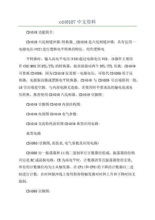
cd40107中文资料CD4049功能简介:CD4049六反相缓冲器/转换器.,CD4049是六反相缓冲器,具有仅用一电源电压(VCC)进行逻辑电平转换的特征。
用作逻辑电平转换时,输入高电平电压(VIH)超过电源电压VCD。
该器件主要用作COS/MOS到DTL/TTL的转换器,能直接驱动两个DTL/TTL负载。
CD4049可替换CD4009,因为CD4049仅需要一电源电压,可取代CD4009用于反相器、电源驱动器或逻辑电平转换器。
CD4049与CD4009引出端排列一致,16引出端是空脚,与内部电路无连接。
若使用时不要求高的漏电流或电压转换,推荐使用CD4049六反相器。
CD4049引脚图:CD4049引脚图CD4049内部结构图:CD4049内部图CD4049电气参数:CD4049交流特性波形图CD4049典型应用电路:典型电路CD4060(引脚图,真值表,电气参数及应用电路)CD4060由一振荡器和14级二进制串行计数器位组成,振荡器的结构可以是RC或晶振电路,CR为高电平时,计数器清零且振荡器使用无效。
所有的计数器位均为主从触发器。
在CP1(和CP0)的下降沿计数器以二进制进行计数。
在时钟脉冲线上使用斯密特触发器对时钟上升和下降时间无限制。
CD4060引脚图:CD4060引脚功能图CD4060内部结构图:CD4060内部方框图CD4060电气参数:CD4060典型应用电路CD4060B典型振荡器连接:上图-RC振荡器下图-晶体振荡器CD4060秒脉冲发生器电路:图2CD4060秒脉冲发生器脉冲发生器是数字钟的核心部分,它的精度和稳定度决定了数字钟的质量,通常用晶体振荡器发出的脉冲经过整形、分频获得1Hz的秒脉冲。
如晶振为32768Hz,通过15次二分频后可获得1Hz的脉冲输出,电路图如图2所示。
CD4060定时电路由CD4060和CD4027构成的50Hz振荡器电路本振荡器能产生交变的50Hz脉冲方波,其占空比为50%.可供某些反相器电路应用。
CD4013中文资料及应用
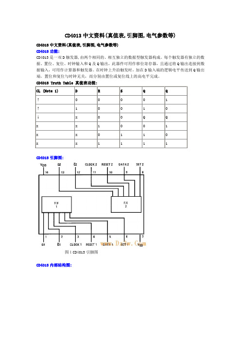
CD4013中文资料(真值表,引脚图,电气参数等)CD4013中文资料(真值表,引脚图,电气参数等)CD4013功能:CD4013是一双D触发器,由两个相同的、相互独立的数据型触发器构成。
每个触发器有独立的数据、置位、复位、时钟输入和Q及Q输出,此器件可用作移位寄存器,且通过将Q输出连接到数据输入,可用作计算器和触发器。
在时钟上升沿触发时,加在D输入端的逻辑电平传送到Q输出端。
置位和复位与时钟无关,而分别由置位或复位线上的高电平完成。
CD4013 Truth Table 真值表功能:CL (Note 1) D R S Q Q↑0 0 0 0 1↑ 1 0 0 1 0↓x 0 0 Q Qx x 1 0 0 1x x 0 1 1 0x x 1 1 1 1CD4013引脚图:图1CD4013引脚图CD4013内部结构图:图2CD4013内部电路图图3 CD4013逻辑图CD4013电气参数:Absolute Maximum Ratings 绝对最大额定值:DC Supply Voltage 直流供电电压 (VDD) -0.5 VDC to +18 VDC Input Voltage输入电压 (VIN) -0.5 VDC to VDD +0.5 VDC Storage Temperature Range储存温度范围 (TS) -65℃ to +150℃Recommended Operating Conditions 建议操作条件:DC Electrical Characteristics 直流电气特性:AC Electrical Characteristics 交流电气特性:图4 切换时间波形CD4013应用电路:图5(左)和图(右)中的CD4013是CMOS双D触发器,这类电路置位和复位信号是高电平有效,由于开关闭合时电容可视为短路而产生高电平,使RD=1,Q=0;若将此信号加到SD,则SD=1,Q=1;置位、复位过后,电容充电而使RD(SD)变为0,电路可进入计数状态。
- 1、下载文档前请自行甄别文档内容的完整性,平台不提供额外的编辑、内容补充、找答案等附加服务。
- 2、"仅部分预览"的文档,不可在线预览部分如存在完整性等问题,可反馈申请退款(可完整预览的文档不适用该条件!)。
- 3、如文档侵犯您的权益,请联系客服反馈,我们会尽快为您处理(人工客服工作时间:9:00-18:30)。
The CD40102B and CD40103B types are supplied in 16-lead dual-in-line plastic packages (E suffix), 16-lead small-outline packages (NSR suffix), and 16-lead thin shrink small-outline packages (PW and PWR suffixes). The CD40103B types also are supplied in 16-lead hermetic dual-in-line ceramic packages (F3A suffix).PACKAGING INFORMATIONOrderable Device Status(1)PackageType PackageDrawingPins PackageQtyEco Plan(2)Lead/Ball Finish MSL Peak Temp(3)CD40102BE ACTIVE PDIP N1625Pb-Free(RoHS)CU NIPDAU N/A for Pkg TypeCD40102BEE4ACTIVE PDIP N1625Pb-Free(RoHS)CU NIPDAU N/A for Pkg TypeCD40102BNSR ACTIVE SO NS162000Green(RoHS&no Sb/Br)CU NIPDAU Level-1-260C-UNLIMCD40102BNSRE4ACTIVE SO NS162000Green(RoHS&no Sb/Br)CU NIPDAU Level-1-260C-UNLIMCD40102BNSRG4ACTIVE SO NS162000Green(RoHS&no Sb/Br)CU NIPDAU Level-1-260C-UNLIMCD40102BPW ACTIVE TSSOP PW1690Green(RoHS&no Sb/Br)CU NIPDAU Level-1-260C-UNLIMCD40102BPWE4ACTIVE TSSOP PW1690Green(RoHS&no Sb/Br)CU NIPDAU Level-1-260C-UNLIMCD40102BPWG4ACTIVE TSSOP PW1690Green(RoHS&no Sb/Br)CU NIPDAU Level-1-260C-UNLIMCD40102BPWR ACTIVE TSSOP PW162000Green(RoHS&no Sb/Br)CU NIPDAU Level-1-260C-UNLIMCD40102BPWRE4ACTIVE TSSOP PW162000Green(RoHS&no Sb/Br)CU NIPDAU Level-1-260C-UNLIMCD40102BPWRG4ACTIVE TSSOP PW162000Green(RoHS&no Sb/Br)CU NIPDAU Level-1-260C-UNLIMCD40103BE ACTIVE PDIP N1625Pb-Free(RoHS)CU NIPDAU N/A for Pkg TypeCD40103BEE4ACTIVE PDIP N1625Pb-Free(RoHS)CU NIPDAU N/A for Pkg Type CD40103BF ACTIVE CDIP J161TBD A42SNPB N/A for Pkg Type CD40103BF3A ACTIVE CDIP J161TBD A42SNPB N/A for Pkg Type CD40103BNSR ACTIVE SO NS162000Green(RoHS&no Sb/Br)CU NIPDAU Level-1-260C-UNLIMCD40103BNSRE4ACTIVE SO NS162000Green(RoHS&no Sb/Br)CU NIPDAU Level-1-260C-UNLIMCD40103BNSRG4ACTIVE SO NS162000Green(RoHS&no Sb/Br)CU NIPDAU Level-1-260C-UNLIMCD40103BPW ACTIVE TSSOP PW1690Green(RoHS&no Sb/Br)CU NIPDAU Level-1-260C-UNLIMCD40103BPWE4ACTIVE TSSOP PW1690Green(RoHS&no Sb/Br)CU NIPDAU Level-1-260C-UNLIMCD40103BPWG4ACTIVE TSSOP PW1690Green(RoHS&no Sb/Br)CU NIPDAU Level-1-260C-UNLIMCD40103BPWR ACTIVE TSSOP PW162000Green(RoHS&no Sb/Br)CU NIPDAU Level-1-260C-UNLIMCD40103BPWRE4ACTIVE TSSOP PW162000Green(RoHS&no Sb/Br)CU NIPDAU Level-1-260C-UNLIMCD40103BPWRG4ACTIVE TSSOP PW162000Green(RoHS&no Sb/Br)CU NIPDAU Level-1-260C-UNLIM(1)The marketing status values are defined as follows:ACTIVE:Product device recommended for new designs.LIFEBUY:TI has announced that the device will be discontinued,and a lifetime-buy period is in effect.NRND:Not recommended for new designs.Device is in production to support existing customers,but TI does not recommend using this part in a new design.PREVIEW:Device has been announced but is not in production.Samples may or may not be available.OBSOLETE:TI has discontinued the production of the device.(2)Eco Plan-The planned eco-friendly classification:Pb-Free(RoHS),Pb-Free(RoHS Exempt),or Green(RoHS&no Sb/Br)-please check /productcontent for the latest availability information and additional product content details.TBD:The Pb-Free/Green conversion plan has not been defined.Pb-Free(RoHS):TI's terms"Lead-Free"or"Pb-Free"mean semiconductor products that are compatible with the current RoHS requirements for all6substances,including the requirement that lead not exceed0.1%by weight in homogeneous materials.Where designed to be soldered at high temperatures,TI Pb-Free products are suitable for use in specified lead-free processes.Pb-Free(RoHS Exempt):This component has a RoHS exemption for either1)lead-based flip-chip solder bumps used between the die and package,or2)lead-based die adhesive used between the die and leadframe.The component is otherwise considered Pb-Free(RoHS compatible)as defined above.Green(RoHS&no Sb/Br):TI defines"Green"to mean Pb-Free(RoHS compatible),and free of Bromine(Br)and Antimony(Sb)based flame retardants(Br or Sb do not exceed0.1%by weight in homogeneous material)(3)MSL,Peak Temp.--The Moisture Sensitivity Level rating according to the JEDEC industry standard classifications,and peak solder temperature.Important Information and Disclaimer:The information provided on this page represents TI's knowledge and belief as of the date that it is provided.TI bases its knowledge and belief on information provided by third parties,and makes no representation or warranty as to the accuracy of such information.Efforts are underway to better integrate information from third parties.TI has taken and continues to take reasonable steps to provide representative and accurate information but may not have conducted destructive testing or chemical analysis on incoming materials and chemicals.TI and TI suppliers consider certain information to be proprietary,and thus CAS numbers and other limited information may not be available for release.In no event shall TI's liability arising out of such information exceed the total purchase price of the TI part(s)at issue in this document sold by TI to Customer on an annual basis.TAPE AND REELINFORMATION*All dimensionsare nominalDevicePackage Type Package Drawing Pins SPQReel Diameter (mm)Reel Width W1(mm)A0(mm)B0(mm)K0(mm)P1(mm)W (mm)Pin1Quadrant CD40102BNSR SO NS 162000330.016.48.210.5 2.512.016.0Q1CD40102BPWR TSSOP PW 162000330.012.47.0 5.6 1.68.012.0Q1CD40103BNSR SO NS 162000330.016.48.210.5 2.512.016.0Q1CD40103BPWRTSSOPPW162000330.012.47.05.61.68.012.0Q1PACKAGE MATERIALS INFORMATION11-Mar-2008*Alldimensions are nominalDevice Package TypePackage DrawingPins SPQ Length (mm)Width (mm)Height (mm)CD40102BNSR SO NS 162000346.0346.033.0CD40102BPWR TSSOP PW 162000346.0346.029.0CD40103BNSR SO NS 162000346.0346.033.0CD40103BPWRTSSOPPW162000346.0346.029.0PACKAGE MATERIALS INFORMATION11-Mar-2008Pack Materials-Page 2元器件交易网IMPORTANT NOTICETexas Instruments Incorporated and its subsidiaries(TI)reserve the right to make corrections,modifications,enhancements,improvements, and other changes to its products and services at any time and to discontinue any product or service without notice.Customers should obtain the latest relevant information before placing orders and should verify that such information is current and complete.All products are sold subject to TI’s terms and conditions of sale supplied at the time of order acknowledgment.TI warrants performance of its hardware products to the specifications applicable at the time of sale in accordance with TI’s standard warranty.Testing and other quality control techniques are used to the extent TI deems necessary to support this warranty.Except where mandated by government requirements,testing of all parameters of each product is not necessarily performed.TI assumes no liability for applications assistance or customer product design.Customers are responsible for their products and applications using TI components.To minimize the risks associated with customer products and applications,customers should provide adequate design and operating safeguards.TI does not warrant or represent that any license,either express or implied,is granted under any TI patent right,copyright,mask work right, or other TI intellectual property right relating to any combination,machine,or process in which TI products or services are rmation published by TI regarding third-party products or services does not constitute a license from TI to use such products or services or a warranty or endorsement e of such information may require a license from a third party under the patents or other intellectual property of the third party,or a license from TI under the patents or other intellectual property of TI.Reproduction of TI information in TI data books or data sheets is permissible only if reproduction is without alteration and is accompanied by all associated warranties,conditions,limitations,and notices.Reproduction of this information with alteration is an unfair and deceptive business practice.TI is not responsible or liable for such altered rmation of third parties may be subject to additional restrictions.Resale of TI products or services with statements different from or beyond the parameters stated by TI for that product or service voids all express and any implied warranties for the associated TI product or service and is an unfair and deceptive business practice.TI is not responsible or liable for any such statements.TI products are not authorized for use in safety-critical applications(such as life support)where a failure of the TI product would reasonably be expected to cause severe personal injury or death,unless officers of the parties have executed an agreement specifically governing such use.Buyers represent that they have all necessary expertise in the safety and regulatory ramifications of their applications,and acknowledge and agree that they are solely responsible for all legal,regulatory and safety-related requirements concerning their products and any use of TI products in such safety-critical applications,notwithstanding any applications-related information or support that may be provided by TI.Further,Buyers must fully indemnify TI and its representatives against any damages arising out of the use of TI products in such safety-critical applications.TI products are neither designed nor intended for use in military/aerospace applications or environments unless the TI products are specifically designated by TI as military-grade or"enhanced plastic."Only products designated by TI as military-grade meet military specifications.Buyers acknowledge and agree that any such use of TI products which TI has not designated as military-grade is solely at the Buyer's risk,and that they are solely responsible for compliance with all legal and regulatory requirements in connection with such use. TI products are neither designed nor intended for use in automotive applications or environments unless the specific TI products are designated by TI as compliant with ISO/TS16949requirements.Buyers acknowledge and agree that,if they use any non-designated products in automotive applications,TI will not be responsible for any failure to meet such requirements.Following are URLs where you can obtain information on other Texas Instruments products and application solutions:Products ApplicationsAmplifiers AudioData Converters AutomotiveDSP BroadbandClocks and Timers Digital ControlInterface MedicalLogic MilitaryPower Mgmt Optical NetworkingMicrocontrollers SecurityRFID TelephonyRF/IF and ZigBee®Solutions Video&ImagingWirelessMailing Address:Texas Instruments,Post Office Box655303,Dallas,Texas75265Copyright©2008,Texas Instruments Incorporated。