TPS62043DGQ中文资料
TPA6204A1

ORDERING INFORMATION6Figure 9Ch1 100 mV/div Ch4 10 mV/div2 ms/divV DDV OUTV o l t a g e − Vt − Time − msPACKAGING INFORMATION Orderable DeviceStatus (1)Package Type Package Drawing Pins Package Qty Eco Plan (2)Lead/Ball Finish MSL Peak Temp (3)TPA6204A1DRBACTIVE SON DRB 8121Green (RoHS &no Sb/Br)CU NIPDAU Level-2-260C-1YEAR TPA6204A1DRBG4ACTIVE SON DRB 8121Green (RoHS &no Sb/Br)CU NIPDAU Level-2-260C-1YEAR TPA6204A1DRBRACTIVE SON DRB 83000Green (RoHS &no Sb/Br)CU NIPDAU Level-2-260C-1YEAR TPA6204A1DRBRG4ACTIVE SON DRB 83000Green (RoHS &no Sb/Br)CU NIPDAU Level-2-260C-1YEAR (1)The marketing status values are defined as follows:ACTIVE:Product device recommended for new designs.LIFEBUY:TI has announced that the device will be discontinued,and a lifetime-buy period is in effect.NRND:Not recommended for new designs.Device is in production to support existing customers,but TI does not recommend using this part in a new design.PREVIEW:Device has been announced but is not in production.Samples may or may not be available.OBSOLETE:TI has discontinued the production of the device.(2)Eco Plan -The planned eco-friendly classification:Pb-Free (RoHS)or Green (RoHS &no Sb/Br)-please check /productcontent for the latest availability information and additional product content details.TBD:The Pb-Free/Green conversion plan has not been defined.Pb-Free (RoHS):TI's terms "Lead-Free"or "Pb-Free"mean semiconductor products that are compatible with the current RoHS requirements for all 6substances,including the requirement that lead not exceed 0.1%by weight in homogeneous materials.Where designed to be soldered at high temperatures,TI Pb-Free products are suitable for use in specified lead-free processes.Green (RoHS &no Sb/Br):TI defines "Green"to mean Pb-Free (RoHS compatible),and free of Bromine (Br)and Antimony (Sb)based flame retardants (Br or Sb do not exceed 0.1%by weight in homogeneous material)(3)MSL,Peak Temp.--The Moisture Sensitivity Level rating according to the JEDEC industry standard classifications,and peak solder temperature.Important Information and Disclaimer:The information provided on this page represents TI's knowledge and belief as of the date that it is provided.TI basesits knowledge and belief on information provided by third parties,and makes no representation or warranty as to the accuracy of such information.Efforts are underway to better integrate information from third parties.TI has taken and continues to take reasonable steps to provide representative and accurate information but may not have conducted destructive testing or chemical analysis on incoming materials and chemicals.TI and TI suppliers consider certain information to be proprietary,and thus CAS numbers and other limited information may not be available for release.In no event shall TI's liability arising out of such information exceed the total purchase price of the TI part(s)at issue in this document sold by TI to Customer on an annual basis.PACKAGE OPTION ADDENDUM 19-May-2005Addendum-Page 1IMPORTANT NOTICETexas Instruments Incorporated and its subsidiaries (TI) reserve the right to make corrections, modifications, enhancements, improvements, and other changes to its products and services at any time and to discontinue any product or service without notice. Customers should obtain the latest relevant information before placing orders and should verify that such information is current and complete. All products are sold subject to TI’s terms and conditions of sale supplied at the time of order acknowledgment.TI warrants performance of its hardware products to the specifications applicable at the time of sale in accordance with TI’s standard warranty. T esting and other quality control techniques are used to the extent TI deems necessary to support this warranty. Except where mandated by government requirements, testing of all parameters of each product is not necessarily performed.TI assumes no liability for applications assistance or customer product design. Customers are responsible for their products and applications using TI components. T o minimize the risks associated with customer products and applications, customers should provide adequate design and operating safeguards.TI does not warrant or represent that any license, either express or implied, is granted under any TI patent right, copyright, mask work right, or other TI intellectual property right relating to any combination, machine, or process in which TI products or services are used. Information published by TI regarding third-party products or services does not constitute a license from TI to use such products or services or a warranty or endorsement thereof. Use of such information may require a license from a third party under the patents or other intellectual property of the third party, or a license from TI under the patents or other intellectual property of TI.Reproduction of information in TI data books or data sheets is permissible only if reproduction is without alteration and is accompanied by all associated warranties, conditions, limitations, and notices. Reproduction of this information with alteration is an unfair and deceptive business practice. TI is not responsible or liable for such altered documentation.Resale of TI products or services with statements different from or beyond the parameters stated by TI for that product or service voids all express and any implied warranties for the associated TI product or service and is an unfair and deceptive business practice. TI is not responsible or liable for any such statements. Following are URLs where you can obtain information on other Texas Instruments products and application solutions:Products ApplicationsAmplifiers Audio /audioData Converters Automotive /automotiveDSP Broadband /broadbandInterface Digital Control /digitalcontrolLogic Military /militaryPower Mgmt Optical Networking /opticalnetwork Microcontrollers Security /securityTelephony /telephonyVideo & Imaging /videoWireless /wirelessMailing Address:Texas InstrumentsPost Office Box 655303 Dallas, Texas 75265Copyright 2005, Texas Instruments Incorporated。
PST620系列数字式变压器保护装置技术说明书

编 写 审 核 批 准
赵永彬 王荣兴 郭效军
V1.10
国电南京自动化股份有限公司
2003 年 4 月
*本说明书可能会被修改 *由国电南自技术部监制 请注意最新版本资料
目
次
1 装置简介.......................................................................................................................................... 1 1.1 装置的功能配置 .................................................................................................................... 1 1.2 装置的特点 ............................................................................................................................ 2 2 性能参数.......................................................................................................................................... 5 2.1 额定参数 ................................................................................................................................ 5 2.2 主要技术性能 ........................................................................................................................ 5 2.3 绝缘性能 ................................................................................................................................ 6 2.4 抗电气干扰性能 .................................................................................................................... 6 2.5 机械性能 ................................................................................................................................ 7 2.6 正常工作大气条件 ................................................................................................................ 7 3 装置硬件.......................................................................................................................................... 8 3.1 机箱结构 ................................................................................................................................ 8 3.2 主要模件设计 ........................................................................................................................ 8 4 PST 621/622 数字式变压器保护 ................................................................................................... 13 4.1 差动保护 .............................................................................................................................. 13 4.2 非电量保护 .......................................................................................................................... 16 5 PST 626 数字式变压器保护 .......................................................................................................... 18 5.1 后备保护 .............................................................................................................................. 18 5.2 测量与控制 .......................................................................................................................... 25 6 装置参数整定 ................................................................................................................................ 27
TPS60204资料
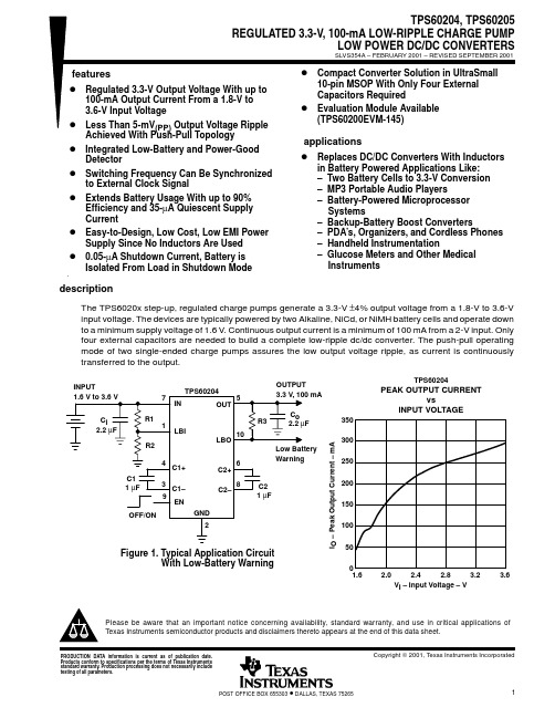
Figure 10t – Time – µs12345678910Figure 1150100150200250300350400450500V OENI It – Time – µsV I = 2.4 VFigure 12LOAD TRANSIENT RESPONSE100 mA10 mA501001502002503003.263.283.303504004505003.24t – Time – µsV I = 2.4 V012345678910t – Time – msFigure 13元器件交易网IMPORTANT NOTICETexas Instruments Incorporated and its subsidiaries (TI) reserve the right to make corrections, modifications,enhancements, improvements, and other changes to its products and services at any time and to discontinueany product or service without notice. Customers should obtain the latest relevant information before placingorders and should verify that such information is current and complete. All products are sold subject to TI’s termsand conditions of sale supplied at the time of order acknowledgment.TI warrants performance of its hardware products to the specifications applicable at the time of sale inaccordance with TI’s standard warranty. Testing and other quality control techniques are used to the extent TIdeems necessary to support this warranty. Except where mandated by government requirements, testing of allparameters of each product is not necessarily performed.TI assumes no liability for applications assistance or customer product design. Customers are responsible fortheir products and applications using TI components. To minimize the risks associated with customer productsand applications, customers should provide adequate design and operating safeguards.TI does not warrant or represent that any license, either express or implied, is granted under any TI patent right,copyright, mask work right, or other TI intellectual property right relating to any combination, machine, or processin which TI products or services are used. Information published by TI regarding third–party products or servicesdoes not constitute a license from TI to use such products or services or a warranty or endorsement thereof.Use of such information may require a license from a third party under the patents or other intellectual propertyof the third party, or a license from TI under the patents or other intellectual property of TI.Reproduction of information in TI data books or data sheets is permissible only if reproduction is withoutalteration and is accompanied by all associated warranties, conditions, limitations, and notices. Reproductionof this information with alteration is an unfair and deceptive business practice. TI is not responsible or liable forsuch altered documentation.Resale of TI products or services with statements different from or beyond the parameters stated by TI for thatproduct or service voids all express and any implied warranties for the associated TI product or service andis an unfair and deceptive business practice. TI is not responsible or liable for any such statements.Mailing Address:Texas InstrumentsPost Office Box 655303Dallas, Texas 75265Copyright 2001, Texas Instruments Incorporated。
天津曙光敬业科技有限公司数字开关说明书

本说明书由天津曙光敬业科技有限公司翻译This manual has been translated by Tianjin Aurora UA V Technology Co.,Ltd.尊敬的用户,欢迎购买我们的数字开关。
此产品是世界上第一个多功能开关系统,由PowerBox Systems GmbH研发、生产。
它专门使用轻巧的锂电池,在接收机电源供应的开关安全性上有很大改善。
此产品外壳坚固并带有一个自锁电子开关、一个高性能线性IC控制稳压电路和一个电压监测器。
此电压监测器使用一个两芯锂电池和一个五芯镍镉/镍氢电池组,分四个阶段进行监测。
重要的构造特点:坚固的塑料外壳(材质为30%的玻璃纤维)、两根连接导线、一根横截面为0.34mm2的硅导线直接焊接在焊接板上(如在同一直线上),焊接板封装在专用的胶层中以防振、SMT安装电路板、编程控制的线路转换程序以及两个散热片(其中一个焊接在电路板上)。
我们建议将数字开关用于以下类型的模型:-带有五个标准尺寸舵机的中小型模型飞机-F3A模型(非常适用于此模型)-带有八个或八个以上舵机的滑翔机,依据舵机尺寸、模型尺寸和飞行类型(热飞行或特技飞行)-电力驱动或光驱动的直升机,转子直径为1.30m,最多带有五个舵机-电力驱动或光驱动的RC模型汽车-模型船-汽油机点火系统的电压为四芯镍镉电池的电压(DA或其它)操作:数字开关由一个按钮控制,操作起来非常简便。
此按钮也用来设置想要安装的电池的开关。
在一般情况下,此按钮负责将开关信号传输给电子开关;按钮本身与实际的电流转换没有关系。
将一个两芯锂电池或一个五芯镍镉/镍氢电池与电池导线连接。
此导线装有一个极化通用接头。
注意,应将电池极性连接正确。
注意:将电池极性接反会损坏开关中的集成稳压器IC。
连接好电池后,LED指示灯会亮起来并显示电池的电压:绿色表示电压正常,橙色表示半放电,红色表示电量不足。
当自锁电子开关连接到电源时,其默认状态为“ON”。
620G 规格书

电流
CH2 CH2
电阻
可选择24 V +/- 10% 或者 28V +/-10% 请参考热电阻相关规格表 0.024 0.0035 0.03 0.004 0.0025 0.008 0.048 0.0035 0.06 0.048 0.0035 0.06 0-400 Ω 5 mA, 400-2000 Ω 1mA, 2000-4000 Ω 0.5 mA 0.0003 0.00023 0.003 0.0003 0.000074 0.003 方波,正振幅最高12V(可调),负振幅 -120mV (固定值) 正弦波和锯齿波,可调幅值 -2.5 +20 V 0 20V +/-20mV (最大6 mA 请参考上面的量程表中对应的频率 请参考上面的量程表中对应的频率 最大计数 1000000. 1个 ~ 50,000
PM620 压力模块
DPI 620/G 多功能校验仪和通讯器
特点
• 集成压力、电信号、温度和频率于一个校验系统 • 完全的HART手操器功能 • 可选的 Foundation Fieldbus • 量程应用模块化和可扩展概念 • 各部件可作为独立的仪器使用 • 显著减少设备数量 • 简化培训和提高操作安全性 • 减少用户成本
输出模式
直流电压 0.014 0.01 0.009* 0.0145 0.015 0.015 0.01 0.005 0.005 0.0035 0.005 0.005 0 0 0 0 0 0 0.0005 0.0005 0.0005 0.0005 0.0005 0.0005 0.001 0.1 0.1 0.001 0.001 0.001 CH1 CH1 CH1 CH1 CH1
+ %FS
%Rdg
HGTP20N60A4;中文规格书,Datasheet资料

HGTG20N60A4, HGTP20N60A4600V, SMPS Series N-Channel IGBTsThe HGTG20N60A4 and HGTP20N60A4 are MOS gated high voltage switching devices combining the best features of MOSFETs and bipolar transistors. These devices have the high input impedance of a MOSFET and the low on-state conduction loss of a bipolar transistor. The much loweron-state voltage drop varies only moderately between 25o C and 150o C.This IGBT is ideal for many high voltage switching applications operating at high frequencies where low conduction losses are essential. This device has been optimized for high frequency switch mode power supplies.Formerly Developmental Type TA49339.Symbol Features•>100kHz Operation at 390V, 20A•200kHz Operation at 390V, 12A•600V Switching SOA Capability•Typical Fall Time. . . . . . . . . . . . . . . . . 55ns at T J = 125o C •Low Conduction Loss•Temperature Compensating SABER™ Model•Related Literature-TB334 “Guidelines for Soldering Surface MountComponents to PC BoardsPackagingJEDEC TO-220AB ALTERNATE VERSIONJEDEC STYLE TO-247Ordering InformationPART NUMBER PACKAGE BRAND HGTP20N60A4TO-220AB20N60A4HGTG20N60A4TO-24720N60A4 NOTE:When ordering, use the entire part number.CEGGCE COLLECTOR(FLANGE)COLLECTOR(FLANGE)CEGAbsolute Maximum Ratings T C = 25o C, Unless Otherwise SpecifiedHGTG20N60A4, HGTP20N60A4UNITS Collector to Emitter Voltage. . . . . . . . . . . . . . . . . . . . . . . . . . . . . . . . . . . . . . . . . . . . . .BV CES600V Collector Current ContinuousAt T C = 25o C . . . . . . . . . . . . . . . . . . . . . . . . . . . . . . . . . . . . . . . . . . . . . . . . . . . . . . . . .I C2570A At T C = 110o C . . . . . . . . . . . . . . . . . . . . . . . . . . . . . . . . . . . . . . . . . . . . . . . . . . . . . . .I C11040A Collector Current Pulsed (Note 1) . . . . . . . . . . . . . . . . . . . . . . . . . . . . . . . . . . . . . . . . . . . I CM280A Gate to Emitter Voltage Continuous. . . . . . . . . . . . . . . . . . . . . . . . . . . . . . . . . . . . . . . . .V GES±20V Gate to Emitter Voltage Pulsed . . . . . . . . . . . . . . . . . . . . . . . . . . . . . . . . . . . . . . . . . . . .V GEM±30V Switching Safe Operating Area at T J = 150o C (Figure 2) . . . . . . . . . . . . . . . . . . . . . . . SSOA100A at 600VPower Dissipation Total at T C = 25o C . . . . . . . . . . . . . . . . . . . . . . . . . . . . . . . . . . . . . . . . .P D290W Power Dissipation Derating T C > 25o C . . . . . . . . . . . . . . . . . . . . . . . . . . . . . . . . . . . . . . . . . . 2.32W/o C Operating and Storage Junction Temperature Range . . . . . . . . . . . . . . . . . . . . . . . . T J, T STG-55 to 150o C Maximum Lead Temperature for SolderingLeads at 0.063in (1.6mm) from Case for 10s. . . . . . . . . . . . . . . . . . . . . . . . . . . . . . . . . . T L Package Body for 10s, See Tech Brief 334 . . . . . . . . . . . . . . . . . . . . . . . . . . . . . . . . .T PKG 300260o Co CCAUTION: Stresses above those listed in “Absolute Maximum Ratings” may cause permanent damage to the device. This is a stress only rating and operation of the device at these or any other conditions above those indicated in the operational sections of this specification is not implied.NOTE:1.Pulse width limited by maximum junction temperature.Electrical Specifications T J = 25o C, Unless Otherwise SpecifiedPARAMETER SYMBOL TEST CONDITIONS MIN TYP MAX UNITS Collector to Emitter Breakdown Voltage BV CES I C = 250µA, V GE = 0V600--V Emitter to Collector Breakdown Voltage BV ECS I C = 10mA, V GE = 0V15--V Collector to Emitter Leakage Current I CES V CE = 600V T J = 25o C--250µAT J = 125o C-- 2.0mACollector to Emitter Saturation Voltage V CE(SAT)I C = 20A,V GE = 15V T J = 25o C- 1.8 2.7V T J = 125o C- 1.6 2.0VGate to Emitter Threshold Voltage V GE(TH)I C = 250µA, V CE = 600V 4.5 5.57.0V Gate to Emitter Leakage Current I GES V GE = ±20V--±250nA Switching SOA SSOA T J = 150o C, R G = 3Ω, V GE = 15VL = 100µH, V CE = 600V100--A Gate to Emitter Plateau Voltage V GEP I C = 20A, V CE = 300V-8.6-VOn-State Gate Charge Q g(ON)I C = 20A,V CE = 300V V GE = 15V-142162nC V GE = 20V-182210nCCurrent Turn-On Delay Time t d(ON)I IGBT and Diode at T J = 25o CI CE = 20AV CE = 390VV GE =15VR G = 3ΩL = 500µHTest Circuit (Figure 20)-15-nsCurrent Rise Time t rI-12-ns Current Turn-Off Delay Time t d(OFF)I-73-ns Current Fall Time t fI-32-ns Turn-On Energy (Note 3)E ON1-105-µJ Turn-On Energy (Note 3)E ON2-280350µJ Turn-Off Energy (Note 2)E OFF-150200µJCurrent Turn-On Delay Time t d(ON)I IGBT and Diode at T J = 125o C I CE = 20A V CE = 390V V GE = 15V R G = 3ΩL = 500µHTest Circuit (Figure 20)-1521ns Current Rise Timet rI -1318ns Current Turn-Off Delay Time t d(OFF)I -105135ns Current Fall Time t fI -5573ns Turn-On Energy (Note 3)E ON1-115-µJ Turn-On Energy (Note 3)E ON2-510600µJ Turn-Off Energy (Note 2)E OFF -330500µJThermal Resistance Junction To Case R θJC--0.43o C/WNOTES:2.Turn-Off Energy Loss (E OFF ) is defined as the integral of the instantaneous power loss starting at the trailing edge of the input pulse and ending at the point where the collector current equals zero (I CE = 0A). All devices were tested per JEDEC Standard No. 24-1 Method for Measurement of Power Device Turn-Off Switching Loss. This test method produces the true total Turn-Off Energy Loss.3.Values for two Turn-On loss conditions are shown for the convenience of the circuit designer. E ON1 is the turn-on loss of the IGBT only. E ON2 is the turn-on loss when a typical diode is used in the test circuit and the diode is at the same T J as the IGBT. The diode type is specified in Figure 20.Electrical SpecificationsT J = 25o C, Unless Otherwise Specified (Continued)PARAMETERSYMBOL TEST CONDITIONSMIN TYP MAX UNITS Typical Performance CurvesUnless Otherwise SpecifiedFIGURE 1.DC COLLECTOR CURRENT vs CASETEMPERATUREFIGURE 2.MINIMUM SWITCHING SAFE OPERATING AREAFIGURE 3.OPERATING FREQUENCY vs COLLECTOR TOEMITTER CURRENTFIGURE 4.SHORT CIRCUIT WITHSTAND TIMET C , CASE TEMPERATURE (o C)I C E , D C C O L L E C T O R C U R R E N T (A )502008040602575100125150100V GE = 15VPACKAGE LIMITDIE CAPABILITYV CE , COLLECTOR TO EMITTER VOLTAGE (V)700600I C E , C O L L E C T O R T O E M I T T E R C U R R E N T (A )2030040020010050060008010040120T J = 150o C, R G = 3Ω, V GE = 15V, L = 100µHf M A X , O P E R A T I N G F R E Q U E N C Y (k H z )5I CE , COLLECTOR TO EMITTER CURRENT (A)40300501020500T J = 125o C, R G = 3Ω, L = 500µH, V CE = 390V 1004030f MAX1 = 0.05 / (t d(OFF)I + t d(ON)I )R ØJC = 0.43o C/W, SEE NOTES P C = CONDUCTION DISSIPATION(DUTY FACTOR = 50%)f MAX2 = (P D - P C ) / (E ON2 + E OFF )T C V GE 15V75o CV GE , GATE TO EMITTER VOLTAGE (V)I S C , P E A K S H O R T C I R C U I T C U R R E N T (A )t S C , S H O R T C I R C U I T W I T H S T A N D T I M E (µs )10111215021010025035045014131446812150200300400V CE = 390V, R G = 3Ω, T J = 125o Ct SCI SCFIGURE 5.COLLECTOR TO EMITTER ON-STATE VOLTAGEFIGURE 6.COLLECTOR TO EMITTER ON-STATE VOLTAGEFIGURE 7.TURN-ON ENERGY LOSS vs COLLECTOR TOEMITTER CURRENT FIGURE 8.TURN-OFF ENERGY LOSS vs COLLECTOR TOEMITTER CURRENTFIGURE 9.TURN-ON DELAY TIME vs COLLECTOR TOEMITTER CURRENT FIGURE 10.TURN-ON RISE TIME vs COLLECTOR TOEMITTER CURRENT0.8 1.2V CE , COLLECTOR TO EMITTER VOLTAGE (V)I C E , C O L L E C T O R T O E M I T T E R C U R R E N T (A )20401.62.03.28060T J = 125o C T J = 150o CPULSE DURATION = 250µsDUTY CYCLE < 0.5%, V GE = 12V 100T J = 25o C0.4 2.4 2.8I C E , C O L L E C T O R T O E M I T T E R C U R R E N T (A )V CE , COLLECTOR TO EMITTER VOLTAGE (V)DUTY CYCLE < 0.5%, V GE = 15V PULSE DURATION = 250µs T J = 150o CT J = 25o CT J = 125o C204080601000.8 1.2 1.6 2.00.4 2.4 2.8E O N 2, T U R N -O N E N E R G Y L O S S (µJ )1000600I CE , COLLECTOR TO EMITTER CURRENT (A)8004001200015102025303540T J = 125o C, V GE = 12V, V GE = 15VR G = 3Ω, L = 500µH, V CE = 390VT J = 25o C, V GE = 12V , V GE = 15V20051400600I CE , COLLECTOR TO EMITTER CURRENT (A)E OF F , T U R N -O F F E N E RG Y L O S S (µJ )100400200500700800T J = 25o C, V GE = 12V OR 15VT J = 125o C, V GE = 12V OR 15V300 R G = 3Ω, L = 500µH, V CE = 390V 151020253035405I CE , COLLECTOR TO EMITTER CURRENT (A)t d (O N )I ,T U R N -O N D E L A Y T I M E (n s )81416182022151020253035405T J = 25o C, T J = 125o C, V GE = 15VT J = 25o C, T J = 125o C, V GE = 12VR G = 3Ω, L = 500µH, V CE = 390V 1210I CE , COLLECTOR TO EMITTER CURRENT (A)t r I ,R I S E T I M E (n s )4820161224363228R G = 3Ω, L = 500µH, V CE = 390VT J = 25o C, T J = 125o C, V GE = 12VT J = 25o C OR T J = 125o C, V GE = 15V151020253035405FIGURE 11.TURN-OFF DELAY TIME vs COLLECTOR TOEMITTER CURRENT FIGURE 12.FALL TIME vs COLLECTOR TO EMITTERCURRENTFIGURE 13.TRANSFER CHARACTERISTICFIGURE 14.GATE CHARGE WAVEFORMSFIGURE 15.TOTAL SWITCHING LOSS vs CASETEMPERATUREFIGURE 16.TOTAL SWITCHING LOSS vs GATE RESISTANCE806070I CE , COLLECTOR TO EMITTER CURRENT (A)t d (O F F )I , T U R N -O F F D E L A Y T I M E (n s )12010011090V GE = 12V, V GE = 15V , T J = 25o CV GE = 12V, V GE = 15V , T J = 125o CR G = 3Ω, L = 500µH, V CE = 390V151020253035405I CE , COLLECTOR TO EMITTER CURRENT (A)t f I , F A L L T I M E (n s )16322448644056R G = 3Ω, L = 500µH, V CE = 390V7280151020253035405T J = 125o C, V GE = 12V OR 15VT J = 25o C, V GE = 12V OR 15V I C E , C O L L E C T O R T O E M I T T E R C U R R E N T (A )801207891012V GE , GATE TO EMITTER VOLTAGE (V)111602002406PULSE DURATION = 250µsDUTY CYCLE < 0.5%, V CE = 10V T J = 125o CT J = -55o CT J = 25o C40V G E , G A T E T O E M I T T E R V O L T A G E (V )Q G , GATE CHARGE (nC)2140410I G(REF) = 1mA, R L = 15Ω, T J = 25o CV CE = 200V V CE = 400V681216V CE = 600V20406080120100140160I CE = 10A00.20.45075100T C , CASE TEMPERATURE (o C)0.61.0125251501.80.8E T O T A L , T O T A L S W I T C H I N G E N E R G Y L O S S (m J )E TOTAL = E ON2 + E OFFR G = 3Ω, L = 500µH, V CE = 390V, V GE = 15V 1.41.21.6I CE = 30AI CE = 20A0.110100R G , GATE RESISTANCE (Ω)131000E T O T A L , T O T A L S W I T C H I N G E N E R G Y L O S S (m J )10T J = 125o C, L = 500µH, V CE = 390V, V GE = 15V E TOTAL = E ON2 + E OFF I CE = 10AI CE = 20A I CE = 30AFIGURE 17.CAPACITANCE vs COLLECTOR TO EMITTERVOLTAGE FIGURE 18.COLLECTOR TO EMITTER ON-STATE VOLTAGEvs GATE TO EMITTER VOLTAGEFIGURE 19.IGBT NORMALIZED TRANSIENT THERMAL RESPONSE, JUNCTION TO CASETest Circuit and WaveformsFIGURE 20.INDUCTIVE SWITCHING TEST CIRCUIT FIGURE 21.SWITCHING TEST WAVEFORMSV CE , COLLECTOR TO EMITTER VOLTAGE (V)C , C A P A C I T A N C E (n F )2040608010013452FREQUENCY = 1MHzC IESC OES C RES V GE , GATE TO EMITTER VOLTAGE (V)891.710121.82.01.911131415162.12.2V C E , C O L L E C T O R T O E M I T T E R V O L T A G E (V )I CE = 30A I CE = 20AI CE = 10ADUTY CYCLE < 0.5%, T J = 25o C PULSE DURATION = 250µs,t 1,RECTANGULAR PULSE DURATION (s)Z θJ C ,N O R M A L I Z E D T H E R M A L R E S P O N S E10-210-110010-510-310-210-110010-4t 1t 2P DDUTY FACTOR, D = t 1 / t 2PEAK T J = (P D X Z θJC X R θJC ) + T CSINGLE PULSE0.10.20.50.050.010.02R G = 3ΩL = 500µHV DD = 390V+-HGTG20N60A4D DUTDIODE TA49372t fIt d(OFF)It rI t d(ON)I10%90%10%90%V CEI CEV GEE OFFE ON2Handling Precautions for IGBTsInsulated Gate Bipolar T ransistors are susceptible togate-insulation damage by the electrostatic discharge of energy through the devices. When handling these devices, care should be exercised to assure that the static charge built in the handler’s body capacitance is not discharged through the device. With proper handling and application procedures, however, IGBTs are currently being extensively used in production by numerous equipment manufacturers in military, industrial and consumer applications, with virtually no damage problems due to electrostatic discharge. IGBTs can be handled safely if the following basic precautions are taken:1.Prior to assembly into a circuit, all leads should be keptshorted together either by the use of metal shortingsprings or by the insertion into conductive material such as “ECCOSORBD™ LD26” or equivalent.2.When devices are removed by hand from their carriers,the hand being used should be grounded by any suitable means - for example, with a metallic wristband.3.Tips of soldering irons should be grounded.4.Devices should never be inserted into or removed fromcircuits with power on.5.Gate Voltage Rating - Never exceed the gate-voltagerating of V GEM. Exceeding the rated V GE can result in permanent damage to the oxide layer in the gate region.6.Gate Termination - The gates of these devices areessentially capacitors. Circuits that leave the gateopen-circuited or floating should be avoided. Theseconditions can result in turn-on of the device due tovoltage buildup on the input capacitor due to leakagecurrents or pickup.7.Gate Protection - These devices do not have an internalmonolithic Zener diode from gate to emitter. If gateprotection is required an external Zener is recommended.Operating Frequency InformationOperating frequency information for a typical device (Figure3) is presented as a guide for estimating device performance for a specific application. Other typical frequency vs collector current (I CE) plots are possible using the information shown for a typical unit in Figures 6, 7, 8, 9 and 11. The operating frequency plot (Figure 3) of a typical device shows f MAX1 or f MAX2; whichever is smaller at each point. The information is based on measurements of a typical device and is bounded by the maximum rated junction temperature.f MAX1 is defined by f MAX1 = 0.05/(t d(OFF)I+ t d(ON)I). Deadtime (the denominator) has been arbitrarily held to 10% of the on-state time for a 50% duty factor. Other definitions are possible. t d(OFF)I and t d(ON)I are defined in Figure 21. Device turn-off delay can establish an additional frequency limiting condition for an application other than T JM.f MAX2 is defined by f MAX2 = (P D - P C)/(E OFF + E ON2). The allowable dissipation (P D) is defined by P D = (T JM - T C)/RθJC. The sum of device switching and conduction losses must not exceed P D. A 50% duty factor was used (Figure 3) and the conduction losses (P C) are approximated byP C=(V CE x I CE)/2.E ON2 and E OFF are defined in the switching waveforms shown in Figure 21. E ON2 is the integral of the instantaneous power loss (I CE x V CE) during turn-on andE OFF is the integral of the instantaneous power loss(I CE x V CE) during turn-off. All tail losses are included in the calculation for E OFF; i.e., the collector current equals zero (I CE = 0).分销商库存信息: FAIRCHILD HGTP20N60A4。
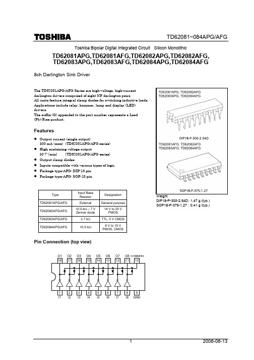
TD62084AFG中文资料
VCE = 2 V, IOUT = 275 mA
⎯
⎯
7.0
VCE = 2 V, IOUT = 350 mA
⎯
⎯
8.0
2 VCE = 2 V, IOUT = 350 mA
1000 ⎯
⎯
Ta = 25°C 6
Ta = 85°C
(Note) ⎯ (Note) ⎯
⎯
50
µA
⎯ 100
Clamp diode forward voltage Input capacitance Turn-on delay Turn-off delay
Test Circuit 1. ICEX
Open VIN
TD62081~084APG/AFG
Open
ICEX
2. VCE (sat), hFE
Open
IIN
IOUT
3. IIN (ON)
IIN (ON)
VCE
VCE, VCE (sat)
VIN
hFE =
IOUT IIN
Open Open
4. IIN (OFF)
123456789 I1 I2 I3 I4 I5 I6 I7 I8 GND
1
2006-06-13
元器件交易网
Schematics (each driver)
TD62081~084APG/AFG
TD62081APG/AFG Common
TD62082APG/AFG Common
−40 to 85 −55 to 150
Unit V
mA/ch V mA V mA
W
°C °C
2
2006-06-13
元器件交易网
深圳市奎达电子 CDT6204 说明书

Condition
Min. Typ. Max. Units
2.5
5.5
V
@VDD = 5V
0.7VDD
VDD
V
@VDD = 5V
0
0.3VDD V
@VDD = 5V , no load @VDD = 3V , no load
720
µA 400
@VDD = 5V , no load @VDD = 3V , no load
腳位圖(Pin Assignment)
OPS 1 SLEEPB 2
VSS 3 OUT4/CLOCK 4
OUT3/DATA 5 OUT2/DIR- 6 OUT1/DIR+ 7
SOP14
14 OSCI 13 MODE/S1 12 VDD 11 INP4 10 INP3 9 INP2 8 INP1
腳位說明(Pin Description)
OPS+R VSS VSS VSS VSS
MODE
VSS
VDD
- -
MODE+R
- -
VSS
VDD
Direct output Active Low, Push-Pull Direct output Active High, Push-Pull Direct output Active Low, Open-Drain
MODE
OPS
VSS
VSS
Active Low, Overtime, Push-Pull
VSS
VDD
Active Low, Unlimited, Push-Pull
VDD
VSS
Active High, Overtime, Push-Pull
- 1、下载文档前请自行甄别文档内容的完整性,平台不提供额外的编辑、内容补充、找答案等附加服务。
- 2、"仅部分预览"的文档,不可在线预览部分如存在完整性等问题,可反馈申请退款(可完整预览的文档不适用该条件!)。
- 3、如文档侵犯您的权益,请联系客服反馈,我们会尽快为您处理(人工客服工作时间:9:00-18:30)。
ORDERING INFORMATION T A
Figure 10
50 µs/div
V I = 3.6 V V O = 1.8 V
PWM/PFM Operation
Figure 11
500 ns/div
Figure 12
POWER SAVE MODE
2.5 µs/div
Figure 13
START-UP
200 µs/div
V I = 3.6 V V O = 1.8 V I O = 1.1 A
元器件交易网
IMPORTANT NOTICE
Texas Instruments Incorporated and its subsidiaries (TI) reserve the right to make corrections, modifications,
enhancements, improvements, and other changes to its products and services at any time and to discontinue
any product or service without notice. Customers should obtain the latest relevant information before placing
orders and should verify that such information is current and complete. All products are sold subject to TI’s terms
and conditions of sale supplied at the time of order acknowledgment.
TI warrants performance of its hardware products to the specifications applicable at the time of sale in
accordance with TI’s standard warranty. T esting and other quality control techniques are used to the extent TI
deems necessary to support this warranty. Except where mandated by government requirements, testing of all
parameters of each product is not necessarily performed.
TI assumes no liability for applications assistance or customer product design. Customers are responsible for
their products and applications using TI components. T o minimize the risks associated with customer products
and applications, customers should provide adequate design and operating safeguards.
TI does not warrant or represent that any license, either express or implied, is granted under any TI patent right,
copyright, mask work right, or other TI intellectual property right relating to any combination, machine, or process
in which TI products or services are used. Information published by TI regarding third-party products or services
does not constitute a license from TI to use such products or services or a warranty or endorsement thereof.
Use of such information may require a license from a third party under the patents or other intellectual property
of the third party, or a license from TI under the patents or other intellectual property of TI.
Reproduction of information in TI data books or data sheets is permissible only if reproduction is without
alteration and is accompanied by all associated warranties, conditions, limitations, and notices. Reproduction
of this information with alteration is an unfair and deceptive business practice. TI is not responsible or liable for
such altered documentation.
Resale of TI products or services with statements different from or beyond the parameters stated by TI for that
product or service voids all express and any implied warranties for the associated TI product or service and
is an unfair and deceptive business practice. TI is not responsible or liable for any such statements.
Following are URLs where you can obtain information on other Texas Instruments products and application
solutions:
Products Applications
Amplifiers Audio /audio
Data Converters Automotive /automotive
DSP Broadband /broadband
Interface Digital Control /digitalcontrol
Logic Military /military
Power Mgmt Optical Networking /opticalnetwork
Microcontrollers Security /security
Telephony /telephony
Video & Imaging /video
Wireless /wireless
Mailing Address:Texas Instruments
Post Office Box 655303 Dallas, Texas 75265
Copyright 2004, Texas Instruments Incorporated。