CXL1517中文资料
ITT CANNON连接器手册中文版

冲压成形加工 36
冲压成形加工 37-38
机械加工 42
传感器器型号2 插座
铜合金镀银
19芯 插头
19芯
法兰插座/锁紧螺母 /线对线
铜合金镀锡、镀银、 铜合金镀锡、镀银、
镀金
镀金
机械加工 43
冲压成形加工 45
冲压成形加工 46-48
APD / ISO 15170
系列 类型
插针材料
插针型号 页码
37芯 插头
RoHS合规信息
ITT在全球所有的电子元件工厂实施了严格的产品控制 计划,使得Cannon、VEAM和BIW连接器产品系列满足欧 盟指令2002/95/EC(又称“减少有害物质”计划)的要求, 对于适当、具体的Cannon、VEAM或BIW产品,订购时可 以为产品编号加上前缀R,确保我们的客户收到符合RoHS 的产品,应用于其商业电子元件和设备中。由于大多数的 RoHS有害物质集中在特定的金属镀层和铅焊涂层上,符合 RoHS的ITT产品提供以下镀层精饰:非电镀镍,不锈钢, 阳极氧化铝和镀金。请注意,在订购板载连接器时,我们 推荐使用镀金替代锡铅焊接。
1/2芯连接器的应用包括: •起重机 •船上厨房 •天线和基站的电力供应
电力分配: •卡车 •牵引车
电气参数
工作电压 工作电流 接触电阻 耐电压 绝缘电阻
机械参数 耐用性 插合扭矩 静负荷,自由状态
48 VDC* 请看温度-电流曲线 0,4mΩ(最大) 1000VAC, 60秒 10 MΩ(最小)
50次插配循环 2Nm(最大) 350 N (ISO 15170-2, Sec. 4.6)
Cannon ҹBKAD/E㋏߫ ᠽሩᴎᶊ䴶ᵓ 䖲఼ˈᓎゟњ 㟾ぎϞⱘ䞠
FPGA可编程逻辑器件芯片XCZU7EV-2FFVF1517I中文规格书

CoolRunner-II Serial Peripheral Interface MasterThe receive full flag (RCV_FULL) is set whenever data is loaded from the SPI receive shiftregister to the SPIRR. This signal is clocked from the system clock and is reset whenever theμC reads data from the SPIRR.SCK Clock LogicThis process generates the SCK output based on the CLKDIV, CPHA, and CPOL settings inthe SPI control register. The clock frequency of the SCK signal is determined by dividing downthe input clock based on the entries in the control register. The signal, SCK_INT is the internalSCK used to clock serial data out of the device and is continually generated. The SPI Controlstate machine is synchronized to this internal signal. The signal SCK_1 represents SCK whenCPHA = 1 and the signal SCK_0 represents SCK when CPHA = 0. The SPI control statemachine generates the masks for these clocks (CLK0_MASK, CLK1_MASK) so that the outputSCK has the correct phase relationship with the data and is held in its inactive state when thereis no data to be transferred. A representation of the logic required to generate the SCK signaloutput to the SPI bus is shown in Figure8.Figure 8: SCK Clock Generation LogicSPI Shift RegistersSPI Transmit Shift RegisterThe SPI transmit shift register is an 8-bit loadable shift register containing SPI data. This shiftregister is loaded from the SPI Transmit Register (SPITR) via a load signal generated by theSPI Control state machine and is clocked by the rising edge of SCK_INT. The data shifting outis the MOSI data. Note that in Figure8, SCK_OUT is one SYS_CLK delay from SCK_INT.Therefore, it is necessary to delay the data being shifted out from the SPI transmit shift registerby one SYS_CLK as well so that the relationship between MOSI and SCK_OUT is maintained. XAPP386 (v1.0) December 12, 2002White Paper: CoolRunner-II CPLDs in Cell Phone Handsets/Terminals But what about new applications that are not in this group? There are applications yet to come that we can envision, but whose exact specifications we cannot wholly anticipate. Designing for their arrival is sometimes called “future proofing.”It is true that some applications are better served by microprocessor code dropped into on board EPROM, but that can only happen as long as the processor bandwidth is available for the application. If this cannot be done, either more processors or additional silicon needs to be added. Either way, the application will need to interface into the phone bus network, and that will require programmable logic, very low power programmable logic.MediPhone—A Speculative Example To drive home some of these ideas, consider an idea for a product that probably does not exist today, but easily could in the near future. It will be marketed under the name “MediPhone” and will target segments of the population that require quick medical support. This would include the growing population of elderly citizens (frequently with enough money to buy these) as well as handicapped people needing close monitoring. See Figure4 for an “artist” conception of this futuristic phone.MediPhone works like this:1. A heart attack (or other medical emergency occurs)2.The victim or friend dials Emergency (911 in the U.S.)3.Personnel receiving the call at a medical facility recognize the phone is“MediPhone” equipped and extract the geographic location of the emergency using GPS4.The medic directs the friend to place the cell phone on the victim’s face5. A video camera scans the Iris for dilation to determine shock level6.The friend is directed to attach small electrodes to the forehead/ear and chest ofthe victim, where pulse is taken and EEG/EKG measurements are driven into the Internet. Everything is attached to the phone.Figure 4:MediPhone Block DiagramWP198 (v1.1) July 4, 2005。
EL817中文资料(everlight)中文数据手册「EasyDatasheet - 矽搜」
和outpu(u维t 索= 50 V R0M0S0)
• 爬电距离7e
7.62 mm
• 操作TEMPgERATUR高达re+110
0°C
• 紧凑小外形封装
e
• 无铅并符合RoHS标准.
• UL认证(编号E214129)
• VDE认证(132249号)
• SEMKO一批个准
• NEMKO一批个准
• DEMKO一批个准
SMD选项.
1
芯片中文手册,看全文,戳
数据表
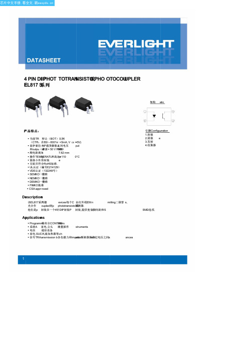
4PIN DIP光电晶体管光耦合器 EL817系列
绝对最大额定值(TA = 25℃)
Input
参数 正向电流
峰值正向电流(1微秒,脉冲)
反向电压
功耗
符号
IF IFP VR
PD
击穿电压
PC
产量
总功耗
隔离电压*
工作温度 储存温度
焊接温度*
集电极电流
• Programm梅布尔CONTRolOlers • 系统A 家电,公头 测量插件 struments • 电信 通信设备 • 家电,SUC风扇加热器等.ch • 信号TRAansmission b各色潜力和impueitdsa断路器操e作nt过电压之间s
ances
引脚Configuuration 1.阳极 2.阴极 e 3.发射 4.收集器
4
芯片中文手册,看全文,戳
数据表
4PIN DIP光电晶体管光耦合器 EL817系列
VCC
IF
IC
RL
产量
Input
脉冲
Input R IN
产量 脉冲
tr ton
图 7.开关时间测试电路和波形
74LVX157MTCX中文资料

© 2003 Fairchild Semiconductor Corporation DS011608May 1993Revised October 200374LVX157 Low Voltage Quad 2-Input Multiplexer74LVX157Low Voltage Quad 2-Input MultiplexerGeneral DescriptionThe LVX157 is a high-speed quad 2-input multiplexer. Four bits of data from two sources can be selected using the common Select and Enable inputs. The four outputs present the selected data in the true (noninverted) form.The LVX157 can also be used as a function generator.Featuress Input voltage level translation from 5V to 3V s Ideal for low power/low noise 3.3V applicationss Guaranteed simultaneous switching noise level and dynamic threshold performanceOrdering Code:Devices are also available in Tape and Reel. Specify by appending letter suffix “X” to the ordering code.Logic Symbols IEEE/IECConnection DiagramPin DescriptionsOrder Number Package NumberPackage Description74LVX157M M16A 16-Lead Small Outline Integrated Circuit (SOIC), JEDEC MS-012, 0.150" Narrow 74LVX157SJ M16D 16-Lead Small Outline Package (SOP), EIAJ TYPE II, 5.3mm Wide74LVX157MTCMTC1616-Lead Thin Shrink Small Outline Package (TSSOP), JEDEC MO-153, 4.4mm WidePin Names DescriptionI 0a –I 0d Source 0 Data Inputs I 1a –I 1d Source 1 Data Inputs E Enable Input S Select Input Z a –Z dOutputs 274L V X 157Truth TableH = HIGH Voltage Level L = LOW Voltage Level X = ImmaterialFunctional DescriptionThe LVX157 is a quad 2-input multiplexer. It selects four bits of data from two sources under the control of a com-mon Select input (S). The Enable input (E) is active-LOW.When E is HIGH, all of the outputs (Z) are forced LOW regardless of all other inputs. The LVX157 is the logic implementation of a 4-pole, 2-position switch where the position of the switch is determined by the logic levels sup-plied to the Select input. The logic equations for the outputs are shown below:Z a = E • (I 1a • S + I 0a • S)Z b = E • (I 1b • S + I 0b • S)Z c = E • (I 1c • S + I 0c • S)Z d = E • (I 1d • S + I 0d • S)A common use of the LVX157 is the moving of data from two groups of registers to four common output busses. The particular register from which the data comes is determined by the state of the Select input. A less obvious use is as a function generator. The LVX157 can generate any four of the sixteen different functions of two variables with one variable common. This is useful for implementing gating functions.Logic DiagramInputsOutputsES I 0I 1Z H X X X L L H X L L L H X H H L L L X LLLHXH74LVX157Absolute Maximum Ratings (Note 1)Recommended Operating Conditions (Note 2)Note 1: The “Absolute Maximum Ratings ” are those values beyond which the safety of the device cannot be guaranteed. The device should not be operated at these limits. The parametric values defined in the Electrical Characteristics tables are not guaranteed at the absolute maximum ratings.The “Recommended Operating Conditions ” table will define the conditions for actual device operation.Note 2: Unused inputs must be held HIGH or LOW. They may not float.DC Electrical CharacteristicsNoise Characteristics (Note 3)Note 3: Input t r = t f = 3nsSupply Voltage (V CC )−0.5V to +7.0VDC Input Diode Current (I IK )V I = −0.5V −20 mADC Input Voltage (V I )−0.5V to 7VDC Output Diode Current (I OK )V O = −0.5V −20 mA V O = V CC + 0.5V +20 mADC Output Voltage (V O )−0.5V to V CC + 0.5VDC Output Source or Sink Current (I O )±25 mA DC V CC or Ground Current (I CC or I GND )±50 mAStorage Temperature (T STG )−65°C to +150°CPower Dissipation180 mWSupply Voltage (V CC ) 2.0V to 3.6V Input Voltage (V I )0V to 5.5V Output Voltage (V O )0V to V CCOperating Temperature (T A )−40°C to +85°C Input Rise and Fall Time (∆t/∆V)0 ns/V to 100 ns/VSymbol ParameterV CC T A = +25°C T A = −40°C to +85°CUnitsConditionsMin TypMaxMin MaxV IHHIGH Level 2.0 1.5 1.5Input Voltage3.0 2.0 2.0V3.6 2.42.4V ILLOW Level 2.00.50.5Input Voltage3.00.80.8V 3.60.80.8V OHHIGH Level 2.0 1.9 2.0 1.9 V IN = V IL or V IH I OH = −50 µAOutput Voltage3.0 2.9 3.02.9VI OH = −50 µA3.0 2.582.48I OH = −4 mAV OLLOW Level 2.00.00.10.1V IN = V IL or V IH I OL = 50 µAOutput Voltage3.00.00.10.1V I OL = 50 µA 3.00.360.44I OL = 4 mAI IN Input Leakage Current 3.6±0.1 ±1.0 µA V IN = 5.5V or GND I CCQuiescent Supply Current3.64.040.0µA V IN = V CC or GND Symbol ParameterV CC T A = 25°C Units C L (pF) (V)Typ Limit V OLP Quiet Output Maximum Dynamic V OL 3.30.30.5V 50V OLV Quiet Output Minimum Dynamic V OL3.3−0.3−0.5V 50V IHD Minimum HIGH Level Dynamic Input Voltage 3.3 2.0V 50V ILDMaximum LOW Level Dynamic Input Voltage3.30.8V50 474L V X 157AC Electrical CharacteristicsNote 4: Parameter guaranteed by design. t OSLH = |t PLHm − t PLHn |.t OSHL = |t PHLm − t PHLn |.CapacitanceNote 5: C PD is defined as the value of the internal equivalent capacitance which is calculated from the operating current consumption without load.Average operating current can be obtained by the equation: I CC(opr.) = C PD × V CC × f IN + I CCSymbol ParameterV CC T A = +25°C T A = −40°C to +85°CUnitsC L (pF)(V)MinTyp Max Min Max t PLH Propagation 2.76.612.5 1.015.5ns 15t PHLDelay Time 9.116.0 1.019.050I n to Z n3.3 ± 0.3 5.17.9 1.09.515 7.611.4 1.013.050t PLH Propagation 2.78.916.9 1.020.5ns 15t PHLDelay Time 11.420.4 1.024.050S to Z n3.3 ± 0.3 7.011.0 1.013.015 9.514.5 1.016.550t PLH t PHLPropagation 2.7 9.117.6 1.020.5ns 15Delay Time 11.621.1 1.024.050 E to Z n3.3 ± 0.37.211.5 1.013.515 9.715.0 1.017.050t OSHL Output to Output 2.7 1.5 1.5ns 50t OSLHSkew (Note 4)3.3 1.51.5Symbol ParameterT A = +25°C T A = −40°C to +85°CUnits MinTyp Max MinMax C IN Input Capacitance4 1010pF C PDPower Dissipation Capacitance (Note 5)20pF 74LVX157Physical Dimensions inches (millimeters) unless otherwise noted16-Lead Small Outline Integrated Circuit (SOIC), JEDEC MS-012, 0.150" NarrowPackage Number M16A 674L V X 157Physical Dimensionsinches (millimeters) unless otherwise noted (Continued)16-Lead Small Outline Package (SOP), EIAJ TYPE II, 5.3mm WidePackage Number M16D774LVX157 Low Voltage Quad 2-Input MultiplexerPhysical Dimensions inches (millimeters) unless otherwise noted (Continued)16-Lead Thin Shrink Small Outline Package (TSSOP), JEDEC MO-153, 4.4mm WidePackage Number MTC16Fairchild does not assume any responsibility for use of any circuitry described, no circuit patent licenses are implied and Fairchild reserves the right at any time without notice to change said circuitry and specifications.LIFE SUPPORT POLICYFAIRCHILD ’S PRODUCTS ARE NOT AUTHORIZED FOR USE AS CRITICAL COMPONENTS IN LIFE SUPPORT DEVICES OR SYSTEMS WITHOUT THE EXPRESS WRITTEN APPROVAL OF THE PRESIDENT OF FAIRCHILD SEMICONDUCTOR CORPORATION. As used herein:1.Life support devices or systems are devices or systems which, (a) are intended for surgical implant into the body, or (b) support or sustain life, and (c) whose failure to perform when properly used in accordance with instructions for use provided in the labeling, can be rea-sonably expected to result in a significant injury to the user.2. A critical component in any component of a life support device or system whose failure to perform can be rea-sonably expected to cause the failure of the life support device or system, or to affect its safety or effectiveness.。
FPGA可编程逻辑器件芯片XCVU3P-1FFVC1517C中文规格书

9.Double-click the Debug Bridge IP identified as xvc_vsec to view the configuration optionfor this IP. Make note of the following configuration parameters because they will be used to configure the driver.•PCIe XVC VSEC ID (default 0x0008)•PCIe XVC VSEC Rev ID (default 0x0)IMPORTANT! Do not modify these parameter values when using a Xilinx Vendor ID or provided XVCdrivers and software. These values are used to detect the XVC extended capability. (See the PCIespecification for additional details.)10.In the Flow Navigator, click Generate Bitstream to generate a bitstream for the exampledesign project. This bitstream will be then be loaded onto the FPGA board to enable XVCdebug over PCIe.After the XVC-over-PCIe hardware design has been completed, an appropriate XVC enabledPCIe driver and associated XVC-Server software application can be used to connect the Vivado Design Suite to the PCIe connected FPGA. Vivado can connect to an XVC-Server application that is running local on the same Machine or remotely on another machine using a TCP/IP socket.System Bring-UpThe first step is to program the FPGA and power on the system such that the PCIe link isdetected by the host system. This can be accomplished by either:•Programming the design file into the flash present on the FPGA board, or•Programming the device directly via JTAG.If the card is powered by the Host PC, it will need to be powered on to perform thisprogramming using JTAG and then re-started to allow the PCIe link to enumerate. After thesystem is up and running, you can use the Linux lspci utility to list out the details for theFPGA-based PCIe device.Compiling and Loading the DriverThe provided PCIe drivers and software should be customized to a specific platform. T oaccomplish this, drivers and software are normally developed to verify the Vendor ID, Device ID, Revision ID, Subsystem Vendor ID, and Subsystem ID before attempting to access device-extended capabilities or peripherals like the PCIe-XVC-VSEC or AXI-XVC. Because the provided driver is generic, it only verifies the Vendor ID and Device ID for compatibility before attempting to identify the PCIe-XVC-VSEC or AXI-XVC peripheral.The XVC driver and software are provide as a ZIP file included with the Vivado Design Suiteinstallation.Appendix D: Using the Xilinx Virtual Cable to DebugPG195 (v4.1) April 29, 2021DMA/Bridge Subsystem for PCIe v4.1Figure 35:XVC-over-PCIe with PCIe Extended Capability InterfaceNote : Although the previous figure shows the UltraScale+™ Devices Integrated Block for PCIe IP, other PCIe IP (that is, the UltraScale™ Devices Integrated Block for PCIe, AXI Bridge for PCIe, or PCIe DMA IP)can be used interchangeably in this diagram.XVC-over-PCIe Through AXI (AXI-XVC)Using the AXI-XVC approach, the Debug Bridge IP connects to the PCIe IP through an AXIInterconnect IP. The Debug Bridge IP connects to the AXI Interconnect like other AXI4-Lite Slave IPs and similarly requires that a specific address range be assigned to it. Traditionally thedebug_bridge IP in this configuration is connected to the control path network rather than the system datapath network. The following figure describes the connectivity between the DMA Subsystem for PCIe IP and the Debug Bridge IP for this implementation.Figure 36:XVC over PCIe with AXI4-Lite InterfaceNote : Although the previous figure shows the PCIe DMA IP, any AXI-enabled PCIe IP can be used interchangeably in this diagram.The AXI-XVC implementation allows for higher speed transactions. However, XVC debug traffic passes through the same PCIe ports and interconnect as other PCIe control path traffic, making it more difficult to debug transactions along this path. As result the AXI-XVC debug should be used to debug a specific peripheral or a different AXI network rather than attempting to debug datapaths that overlap with the AXI-XVC debug communication path.Appendix D: Using the Xilinx Virtual Cable to DebugPG195 (v4.1) April 29, 2021DMA/Bridge Subsystem for PCIe v4.1。
FPGA可编程逻辑器件芯片XCVU065-2FFVC1517I中文规格书

Recommended PCB Design Rules for BGA PackagesBGA PackagesXilinx provides the diameter of a land pad on the package side. This information is required prior to the start of the board layout so the board pads can be designed to match the component-side land geometry. The typical values of these land pads are described in Figure 8-1 and summarized in Table 8-1. PCB pad size is based on the BGA ball size. Typical requirements for the PCB pad size are 80-120% of ball size however, given a large package size and to prevent solder bridging, a pad size closer to 80% of the ball size isrecommended. For Xilinx BGA packages, non-solder mask defined (NSMD) pads on the board are suggested to allow a clearance between the land metal (diameter L) and the solder mask opening (diameter M) as shown in Figure 8-1.Figure 8-1:Suggested Board Layout of Soldered Pads for BGA PackagesUG575_c8_01_102213Packaging OverviewIntroduction to the UltraScale ArchitectureThe Xilinx® UltraScale™ architecture is the first ASIC-class architecture to enablemulti-hundred gigabit-per-second levels of system performance with smart processing,while efficiently routing and processing data on-chip. UltraScale architecture-based devices address a vast spectrum of high-bandwidth, high-utilization system requirements by using industry-leading technical innovations, including next-generation routing, ASIC-likeclocking, 3D-on-3D ICs, multiprocessor SoC (MPSoC) technologies, and new powerreduction features. The devices share many building blocks, providing scalability acrossprocess nodes and product families to leverage system-level investment across platforms.Virtex® UltraScale+™ devices provide the highest performance and integration capabilities in a FinFET node, including both the highest serial I/O and signal processing bandwidth, as well as the highest on-chip memory density. As the industry's most capable FPGA family, the Virtex UltraScale+ devices are ideal for applications including 1+Tb/s networking and data center and fully integrated radar/early-warning systems.Virtex UltraScale devices provide the greatest performance and integration at 20nm,including serial I/O bandwidth and logic capacity. As the industry's only high-end FPGA at the 20nm process node, this family is ideal for applications including 400G networking, large scale ASIC prototyping, and emulation.Kintex® UltraScale+ devices provide the best price/performance/watt balance in a FinFET node, delivering the most cost-effective solution for high-end capabilities, includingtransceiver and memory interface line rates as well as 100G connectivity cores. Our newest mid-range family is ideal for both packet processing and DSP-intensive functions and is well suited for applications including wireless MIMO technology, Nx100G networking, and data center.Kintex UltraScale devices provide the best price/performance/watt at 20nm and include the highest signal processing bandwidth in a mid-range device, next-generationtransceivers, and low-cost packaging for an optimum blend of capability andcost-effectiveness. The family is ideal for packet processing in 100G networking and data centers applications as well as DSP-intensive processing needed in next-generation medical imaging, 8k4k video, and heterogeneous wireless infrastructure.Solder PasteSolder paste consists of solder alloy and a flux system. A typical solder paste composition by volume is split between about 50% alloy and 50% flux. The metal load mass (solder alloy powder) is around 90%, with the remaining 10% mass a flux system. The primary purpose of the flux system is to remove the contaminations from the solder joints during the soldering process. The capability of removing contaminations is determined by the activation level of the type of solder paste. The preferred solder paste metal alloy has a lead-free composition (SnAgCu where Ag is 3–4% and Cu is 0.5–1%). A no-clean solder paste is preferred to eliminate any risk of improper cleaning that could leave active residue beneath the device and other BTC components. The paste must be suitable for printing the solder stencil aperture dimensions. Type 4 paste is recommended for better paste release performance. When using a solder paste, you must adhere to the handling recommendations of the paste manufacturer.Chapter 8:Recommended PCB Design Rules for BGA PackagesFlip-Chip BGA Packages1.0 mm Pitch0.8 mm PitchDesign RuleDimensions in mm (mils)Package land pad opening (SMD)0.53 mm (20.9 mils)0.40 mm (15.7 mils)Maximum PCB solder land (L) diameter 0.50 mm (19.7 mils)0.40 mm (15.7 mils)Opening in PCB solder mask (M) diameter 0.65 mm (25.6 mils)0.50 mm (19.7 mils)Solder ball land pitch (e)1.00 mm (39.4 mils)0.80 mm (31.5 mils)BGA PackageBGA Solder BallSolder MaskPCBUG358_aA_02_110513。
正芯 LX1527 学习码编码芯片 说明书

网址:LX1527 说明书概述LX1527 是一片由CMOS 设计制造的可预烧内码的学习码编码IC ,由软件解码;内码共有20 个位元可预烧1048576 组内码组合,降低使用上的重码率。
主要特点 脚位图2 .工作电压3 . 四个按键组合输入,最多可组合至155 .小体积8 脚SOP 封装,是LX2260的升级产品;6 .与 EV1527、RT1527 完全兼容;管脚说明符号描述管脚I / OOSCI振荡线路输入脚,接电阻至电源1IVCC电源正2CND电源负3TXD编码输出脚40K0按键输入脚,内含下拉电阻5IKl按键输入脚,内含下拉电阻6IK2按键输入脚,内含下拉电阻7IK3按键输入脚,内含下拉电阻8I极限参数符号 参数 条件范围单位Vcc 电源电压-0.3~15VVI 输入电压-0.3~Vcc+ 0.3VVO 输出电压-0.3~Vcc+ 0.3VTst 储存温度-40 ~125℃Top 工作温度-20 ~70 ℃Pdis 最大功耗 Vcc = 12V(空载)24mW传真:0571-******** 89908492 邮编:310014 网址:电气特性参数 条件符号最小典型最大 单位 工作电压Vcc 2.412 15 V 静态电流 Vcc = 12V,OSC stop ,OutPut Unloaded Isb1.0uA 工作电流 Vcc = 12V ,一个按键输入(一个按键接Vcc)Iop 0.5 1.0mA驱动拉电流 Vcc = 12V,Voh = 6V Ioh 5 mA 驱动灌电流 Vcc = 12V,Vol = 6V Iol 3 mA 工作频率Fop80K Hz输出编码的格式定义:1个CLK=8个 OSC CLOCK同步码内码C0~C19(100万组)D0 D1 D2 D3网址:LX1527与EV1527之间振荡电阻的替换关系(仅供参考):EV1527 LX1527430K 3.3M330K 2.4M300K 2.2M振荡电阻和1位数据宽度(TD)对应表13V 12V 11V 10V 9V 8V 7V 6V 5V 4V 1M 605us 620us 640us 655us 675us 704us 736us 780us 844us 944us 1.2M 792us 814us 834us 854us 876us 914us 956us 1.015ms 1.09ms 1.225ms 1.5M 960us 980us 1.01ms 1.03ms 1.06ms 1.1ms 1.145ms 1.23ms 1.32ms 1.47ms 2M 1.22ms 1.25ms 1.28ms 1.31ms 1.35ms 1.39ms 1.46ms 1.54ms 1.65ms 1.85ms 2.2M 1.31ms 1.34ms 1.37ms 1.41ms 1.45ms 1.5ms 1.57ms 1.66ms 1.79ms 1.99ms 2.4M 1.43ms 1.48ms 1.51ms 1.55ms 1.59ms 1.64ms 1.71ms 1.81ms 1.94ms 2.19ms 2.7M 1.68ms 1.71ms 1.75ms 1.79ms 1.84ms 1.91ms 1.99ms 2.11ms 2.27ms 2.53ms 3M 1.79ms 1.82ms 1.86ms 1.91ms 1.96ms 2.03ms 2.11ms 2.24ms 2.401ms 2.69ms 3.3M 1.995ms 2.035ms 2.085ms 2.135ms 2.195ms 2.265ms 2.365ms 2.505ms 2.705ms 3.01ms传真:0571-******** 89908492 邮编:310014 网址:K0~K3按键组合与输出关系表应用线路图K3 K2 K1 KO D3 D2 D1 DO O O O 1 O O O 1 O O 1 O O O 1 0 O O 1 1 O O 1 1 O 1 O O 0 1 O O O 1 O 1 0 1 O 1 O 1 1 O 0 1 1 0 O 1 1 1 0 1 1 1 1 0 0 0 1 0 0 0 1 0 0 1 1 0 0 1 1 0 1 0 1 0 1 0 1 0 1 1 1 0 1 1 1 1 0 0 1 1 0 0 1 1 0 1 1 1 0 1 1 1 1 0 1 1 1 0 11111111。
FPGA可编程逻辑器件芯片XCVU065-FFVC1517中文规格书

Appendix BUpgradingThis appendix contains information about upgrading to a more recent version of the IP.New ParametersThe following new parameters are added in the IP in the current release.Table 136: New ParametersName Display Name Description Default Valueshared_logic_gtc_7xG2Include Shared Logic (TransceiverGT_COMMON) in example design When selected, includesGT_COMMON block in exampledesign.Falseshared_logic_clk_7xG2Include Shared Logic (Clocking) inexample design When selected, includes Clockblock in example design.Falseshared_logic_both_7xG2Include Shared Logic in core When selected, includes bothGT_COMMON and Clock blocks incore.Falseecc_en Enable ECC Enables ECC. Requires one of theParity option to be turned on.Falseaspm_support ASPM Support optionality Indicates ASPM support is Enabledor Disabled.No_ASPM New PortsThe ports in the following table appear at the boundary when the Internal Shared GT_COMMON and Clocking option is selected in the Shared Logic tab for 7 series Gen2 devices.Table 137: Ports For Shared Logic (Internal Shared GT_COMMON and Clocking Option)Name Direction Width int_dclk_out O 1 bitint_oobclk_out O 1 bitint_pclk_sel_slave I 1 bitint_pclk_out_slave O 1 bitPG195 (v4.1) April 29, 2021DMA/Bridge Subsystem for PCIe v4.1Appendix C: Debugging Answer Records for this subsystem can be located by using the Search Support box on the mainXilinx support web page. T o maximize your search results, use keywords such as:•Product name•T ool message(s)•Summary of the issue encounteredA filter search is available after results are returned to further target the results.Master Answer Record for the DMA/Bridge Subsystem for PCIeAR 65443Technical SupportXilinx provides technical support on the Xilinx Community Forums for this LogiCORE™ IP product when used as described in the product documentation. Xilinx cannot guarantee timing,functionality, or support if you do any of the following:•Implement the solution in devices that are not defined in the documentation.•Customize the solution beyond that allowed in the product documentation.•Change any section of the design labeled DO NOT MODIFY.T o ask questions, navigate to the Xilinx Community Forums.Debug ToolsThere are many tools available to address DMA/Bridge Subsystem for PCIe design issues. It isimportant to know which tools are useful for debugging various situations.Vivado Design Suite Debug FeatureThe Vivado® Design Suite debug feature inserts logic analyzer and virtual I/O cores directly into your design. The debug feature also allows you to set trigger conditions to capture applicationand integrated block port signals in hardware. Captured signals can then be analyzed. Thisfeature in the Vivado IDE is used for logic debugging and validation of a design running in Xilinx®devices.The Vivado logic analyzer is used to interact with the logic debug LogiCORE IP cores, including:•ILA 2.0 (and later versions)PG195 (v4.1) April 29, 2021DMA/Bridge Subsystem for PCIe v4.1。
- 1、下载文档前请自行甄别文档内容的完整性,平台不提供额外的编辑、内容补充、找答案等附加服务。
- 2、"仅部分预览"的文档,不可在线预览部分如存在完整性等问题,可反馈申请退款(可完整预览的文档不适用该条件!)。
- 3、如文档侵犯您的权益,请联系客服反馈,我们会尽快为您处理(人工客服工作时间:9:00-18:30)。
CMOS-CCD Signal ProcessorDescriptionThe CXL1517M/1518M are CMOS-CCD signal processors developed for CCD camera complementary color filter array processing system.CXL1517M452.5-bit ×2, 453.5-bit 1H CCD delay line CXL1518M300.5-bit ×2, 301.5-bit 1H CCD delay line Features•Single 5V power supply•Low power consumption (Typ.)CXL1517M 120mW CXL1518M 75mW•Built-in peripheral circuits•Built-in CDS (Correlated Double Sampling) circuit Functions •Clock driver•Autobias circuit (Center and black) •Pedestal clamp circuit •CDS circuit•Overflow prevention circuitAbsolute Maximum Ratings (Ta = 25°C)•Supply voltage V DD 6V •Operating temperature Topr –10 to +65°C •Storage temperature Tstg –55 to +150°C •Allowable power dissipation P D 500mWRecommended Operating Voltage Range (Ta = 25°C)Supply voltage V DD 4.6 to 5.25V– 1–E91777A78-PSSony reserves the right to change products and specifications without prior notice. This information does not convey any license by any implication or otherwise under any patents or other right. Application circuits shown, if any, are typical examples illustrating the operation of the devices. Sony cannot assume responsibility for any problems arising out of the use of these circuits.CXL1517M/1518M20 pin SOP (Plastic)StructureCMOS-CCDItemSymbol V L V H f CL f CLMin.V SS 0.7 ×V DDTyp.7.164.77Max.0.3 ×V DDV DDUnit V V MHz MHzRemarksNTSC: 455f H CCIR: 454f H NTSC: 910f H /3CCIR: 908f H /3Clock voltage Low Clock voltage High Clock frequencyCXL1517M CXL1518M– 2–Block Diagram and Pin Configuration (Top View)V D DV D DA B O V FV D DV G GIN-B IN-A V S SD L 1X D L 2V S SV S SC D SC LPOUT-COUT-AOUT-B IN-C V SS IN-B ABBL V DD IN-C CLP V DD OUT-C V GG IN-A ABCN V DD XDL1XDL2V SS V SS OUT-ACDS ABOVF OUT-BPin DescriptionPin No.Symbol I/O Description CommentV SSIN-B ABBL V DDIN-C CLPV DD OUT-C V GG OUT-B OUT-A CDSV SSV SS XDL2 XDL1 V DD ABCN ABOVF IN-A —IO—II—OOOOO——II—OOIGNDSignal input B channel (Y)Autobias DC output for Y signalPower supplySignal input C channel (Y)Clamp pulse inputPower supplySignal output C channelOutput circuit bias DC outputSignal output B channelSignal output A channelDC output for CDSGNDGNDClock pulse input 2Clock pulse input 1Power supplyAutobias DC output for C signalAutobias DC output for overflow prevention circuitSignal input A channel (C)AnalogBlack level biasAnalogBlack level biasat no clamp >100k>100kOutput circuitOutput circuitTiming>100k>100kTimingCenter level biasCenter level biasat no clamp >100k1234567891011121314151617181920– 3––CXL1517M/1518ME l e c t r i c a l C h a r a c t e r i s t i c sf C L = 7.16M H z (C X L 1517M )T a = 25°C , V D D = 5.0V , V S S = 0Vf C L = 4.77M H z (C X L 1518M )I t e m A u t o b i a s c e n t e r l e v e l A u t o b i a s b l a c k l e v e l O v e r f l o w p r e v e n t i o n c i r c u i t A u t o b i a s l e v e lC D S s o u r c e l e v e l O u t p u t c i r c u i t b i a s l e v e l C u r r e n t ∗s u p p l yI n s e r t i o n g a i n F r e q u e n c y ∗r e s p o n s eL i n e a r i t y T h e i n s e r t i o n g a i n d i f f e r e n c e b e t w e e n c h a n n e l sL i n e a r i t y d i f f e r e n c e b e t w e e n c h a n n e l s C r o s s -t a l k b e t w e e n c h a n n e l s A B C N A B B LA B O V FC D SV G GI D DI G f GL i n .∆G ∆L B C C R T V 1V 2V 3V 4V 5A 1V 6V 6V 6V 6S y m b o lT e s t p o i n tS W c o n d i t i o n s B i a s c o n d i t i o n sS W 1aaaaab b bc b b b b b a a a b b b b a a a a a a a t o c a t o c a t o ca t o c aa a a a a a aa ab S W 2S W 3S W 4t o 6E 1M i n .4.23.92.61.20.3——–4.5–1.5–1.8004.64.33.02.30.82415–3.5–0.4–0.855114.84.53.33.53.03525———121253VVVVVm Ad Bd B%%%%T y p .M a x .C o n d i t i o n s 20 l o g 20 l o gN o t e 1)N o t e 2)N o t e 3)N o t e 4)R a t i n g s U n i tC X L 1517MC X L 1518MC X L 1517MC X L 1518MB c h →C c hO u t p u t a m p l i t u d e (m V p -p )I n p u t a m p l i t u d e (S I N 100k H z , 100m V p -p )↑↓↑↓V 1A →V 1B ,C →V 2+ 0.25V↓A →V 1B ,C →V 2+ 0.25V O u t p u t a m p l i t u d e (S I N 1M H z , 100m V p -p )O u t p u t a m p l i t u d e (S I N 100k H z , 100m V p -p )∗S t a n d a r d v a l u e s a r e d i f f e r e n t b e t w e e n C X L 1517M a n d C X L 1518M .元器件交易网– 5–Notes)1)Linearity testingFor A channel, set input bias to ABCN – 0.2V first, and then set it to ABCN and ABCN + 0.2V. Then input a sine wave of 100kHz and 100mVp-p, and compare the three output amplitudes. For B channel and C channel, set input bias to ABBL + 0.45V first, and then set it to ABBL + 0.25V and ABBL + 0.05V. Then input a sine wave of 100kHz and 100mVp-p, and compare the three output amplitudes. The maximum output amplitude for the respective A, B and C channels is taken as Sout max and the minimum output amplitude as Sout min. The linearity of the respective channels is defined as: Lin. = ×200 [%]2)Calculation of insertion gain differenceAs the maximum insertion gain among A, B and C channels is taken as Gmax and the minimum as Gmin,the insertion gain difference between channels ∆G as: ∆G = |1 – 10()|×100 [%] 3)Calculation of linearity differenceDefine B channel linearity as L B and C channel linearily as L C we obtain the difference ∆L BC as: ∆L BC = |L B – L C |[%]4)Cross-talk calculation CRTa :The cross-talk value of A channel when B and C channels are inputOUT A -a:The output value of A channel when A channel is input SW3-a, SW4-a, SW5, 6-bOUT A -bc :The output value of A channel when B and C channels are input(Cross-talk component) SW3-a, SW4-b, SW5, 6-a CRTa = ×100 [%]Clock Waveform TimingSout max – Sout min Sout max + Sout minGmax – Gmin 20OUT A -bcOUT A -a(140) ∗∗ The value in brackets is for CXL1517M.– 6–XDL XDL Output AOutput BOutput C Electrical Characteristics Test CircuitApplication CircuitApplication circuits shown are typical examples illustrating the operation of the devices. Sony cannot assume responsibility for any problems arising out of the use of these circuits or for any infringement of third party patent and other right due to same.Package Outline Unit: mmSONY CODE EIAJ CODE JEDEC CODE SOP-20P-L01SOP020-P-0300PACKAGE STRUCTUREPACKAGE MATERIALLEAD TREATMENTLEAD MATERIALPACKAGE MASSCOPPER ALLOYSOLDER PLATINGEPOXY RESIN0.3g20PIN SOP (PLASTIC)12.45 – 0.1+ 0.420110.45 ± 0.1 1.271015.3–.1+.37.9±.46.9+ 0.4– 7–。