模拟集成电路Chapter 3-Single-Stage Amplifiers
《模拟集成电路基础》PPT课件
h
20
P
N
V
PN结的接触电位
(二)PN结的接触电位:
(1).内电场的建立,使PN结 中产生电位差。从而形成接 触电位V(又称为位垒)。
(2).接触电位 V决定于材 料及掺杂浓度:
硅: V=0.7 锗: V=0.2 (3).其电位差用 表示
h
21
(三)PN结的单向导电性
U
I
P
N
扩散
Q(V-U)
1.PN结加正向电压时:
第四节 二极管的应用
h
8
第一节 半导体基础知识
一1.、什半么导是体导的体特、性绝:缘体导、电半导率量导电1级0体率-2,2:为-如110:0-154s金.sc.、mc-m1-1
(1).导体:导电性能良好导量的电级物率,质为银如。1、:0-铜橡9-、胶10铝、2 s。云.c母m-、1 (2).绝缘体:几乎不导电量砷塑的级化料物,镓等质如等。。:。硅、锗、 (3).半导体:导电能力介于导体和半导体之间。
生载流子的扩散运用动下的定结向果移产动生称空
间电荷区耗尽层为(漂多移子运运动动)。
空穴 P
(2).空间电荷区产生建立了内电场 产生载流子定向运动(漂移运动)
N
•当扩散运动↑内电场↑漂移运
动↑扩散运动↓动态平衡。
(3).扩散运动产生扩散电流;漂移运动 产生漂移电流。
•动态平衡时:扩散电流=漂移电流。 PN结内总电流=0。 PN结的宽度一定 。
1.电子空穴对: 电子和空穴是成对产生的.
h
12
两种载流子——电子和空穴
外电场E 的方向
电子流
2.自由电子——载流子:
自由电子
• 在外电场作用下形成电子流(在 导带内运动),
CMOS_Analog_Lec5-Single-Stage Amplifier
Spring 10
CMOS Analog IC Design
5
Single Stage MOS Amplifiers
Spring 10
CMOS Analog IC Design
6
Common Source Topology
• Load types
– Passive: R, L, and C – Active: diode, R, and current source
• Source degeneration improves linearity and output resistance at the cost of gain and voltage headroom.
Spring 10
CMOS Analog IC Design
28
Source Follower
Spring 10
CMOS Analog IC Design
19
Triode Region Load
• Consumes less voltage headroom than a diode connected MOS.
Spring 10
CMOS Analog IC Design
20
Common Source with Source Degeneration
Spring 10
CMOS Analog IC Design
4
Functions of an Amplifier
• An essential block in analog circuits • Increase the signal magnitude
– To drive a load – To overcome the noise of a subsequent stage – To provide logical levels to a digital circuit – To play a critical role in feedback circuit
Chapter1-1-Inturduction & PN Junction[new]
![Chapter1-1-Inturduction & PN Junction[new]](https://img.taocdn.com/s3/m/c2f0b1c2da38376baf1fae9a.png)
Analysis and Design of Analog Integrated Circuits
Chapter 1
* Optical Receivers:
The receivers must process a low-level signal at a very high speed, requiring low-noise broadband circuit design.
Analysis and Design of Analog Integrated Circuits
Chapter 1
Analysis and Design of Analog Integrated Circuits
Instructor: Luo Ping
Luo Ping
2004-7-27
1
Analysis and Design of Analog Integrated Circuits
Luo Ping
2004-7-27
4
Analysis and Design of Analog Integrated Circuits
Chapter 1
Why Analog?
--- The “real” or “physical” world is analog --- Examples:
* * * * * * *
Luo Ping 2004-7-27 15
Analysis and Design of Analog Integrated Circuits
Chapter 1
Analog Design Challenging (cont.)
Digital Design Process:
模拟集成电路设计经典教材
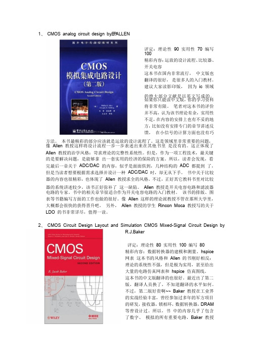
1、 CMOS analog circuit design by P .E.ALLEN评定:理论性 90 实用性 70 编写100精彩内容:运放的设计流程、比较器、开关电容这本书在国内非常流行, 中文版也翻译的很好, 是很多人的入门教材。
建议大家读影印版, 因为 ic 领域的绝大部分文献是以英文写成的。
如果你只能读中文版,你的学习资料将非常有限。
笔者对这本书的评价并不高,认为该书理论有余,认为该书理论有余,实用性实用性不足,在内容的安排上也有不妥的地方,比如没有安排专门的章节讲述反馈, 在小信号的计算方面也没有巧方法。
本书最精彩的部分应该就是运放的设计流程了。
这是领域里非常重要的问题,像 Allen 教授这样将设计流程一步一步表述出来在其他书里 是没有的。
这正体现了 Allen 教授的治学风格:苛求理论的完整性系统性。
但是,作为一项工程技术,最关键的是要解决问题,是能够拿 出一套实用的经济的保险的方案。
所以,读者会发现,看完最后一章关于 ADC/DAC 的内容,似乎是面面俱到,几种结构的 ADC 都提到 了,但是当读者想要根据需求选择并设计一种 ADC/DAC 时,却无从下手。
书中关于比较器的内容也很精彩,器的内容也很精彩,也体现了也体现了 Allen 教授求全的风格。
教授求全的风格。
不过,不过,正好其它教科书里对比较器的系统讲述较少,该书正好弥补了 这一缺陷。
Allen 教授是开关电容电路和滤波器电路的专家。
书中的相关章节很适合作为开关电容电路的入门教材。
该书的排版、图表等书籍编写方面的工作也做的很好。
像 Allen 这样的理论派教授不管在那所大学里,大概都会很快的获得晋升吧。
另外, Allen 教授的学生 Rincon Moca 教授写的关于 LDO 的书非常详尽,值得一读。
2、 CMOS Circuit Design Layout and Simulation CMOS Mixed-Signal Circuit Design byR.J.Baker评定:理论性 80 实用性 100 编写 80精彩内容:数据转换器的建模和测量、hspice网表 这本书的风格和 Allen 的书刚好相反:理论的系统性不强,但是极为实用,甚至给出大量的电路仿真网表和 hspice 仿真图线。
Analysis_of_multistage_amplifier-frequency_compensation
Analysis of Multistage Amplifier–FrequencyCompensationKa Nang Leung and Philip K.T.Mok,Member,IEEEAbstract—Frequency-compensation techniques of single-,two-and three-stage amplifiers based on Miller pole splitting and pole–zero cancellation are reanalyzed.The assumptions made, transfer functions,stability criteria,bandwidths,and important design issues of most of the reported topologies are included. Several proposed methods to improve the published topologies are given.In addition,simulations and experimental results are provided to verify the analysis and to prove the effectiveness of the proposed methods.Index Terms—Damping-factor-control frequency compen-sation,multipath nested Miller compensation,multipath zero cancellation,multistage amplifier,nested Gm-C compensation, nested Miller compensation,simple Miller compensation.I.I NTRODUCTIONM ULTISTAGE amplifiers are urgently needed with the advance in technologies,due to the fact that single-stage cascode amplifier is no longer suitable in low-voltage designs. Moreover,short-channel effect of the sub-micron CMOS transistor causes output-impedance degradation and hence gain of an amplifier is reduced dramatically.Therefore,many frequency-compensation topologies have been reported to stabilize the multistage amplifiers[1]–[26].Most of these topologies are based on pole splitting and pole–zero can-cellation using capacitor and resistor.Both analytical and experimental works have been given to prove the effectiveness of these topologies,especially on two-stage Miller compen-sated amplifiers.However,the discussions in some topologies are focused only on the stability criteria,but detailed design information such as some important assumptions are missing. As a result,if the provided stability criteria cannot stabilize the amplifier successfully,circuit designers usually choose the parameters of the compensation network by trial and error and thus optimum compensation cannot be achieved.In fact,there are not many discussions on the comparison of the existing compensation topologies.Therefore,the differences as well as the pros and cons of the topologies should be inves-tigated in detail.This greatly helps the designers in choosing a suitable compensation technique for a particular design condi-tion such as low-power design,variable output capacitance or variable output current.Manuscript received March9,2000;revised February6,2001.This work was supported by the Research Grant Council of Hong Kong,China under grant HKUST6007/97E.This paper was recommended by Associate Editor N.M.K. Rao.The authors are with the Department of Electrical and Electronic Engineering, The Hong Kong University of Science and Technology,Clear Water Bay,Hong Kong(e-mail:eemok@t.hk).Publisher Item Identifier S1057-7122(01)07716-9.Moreover,practical considerations on the compensation tech-niquesof(a)(b)(c)(d)(e)(f)(g)(h)(i)(j)Fig.1.Studied and proposed frequency-compensation topologies.(a)SMC.(b)SMCNR.(c)MZC.(d)NMC.(e)NMCNR.(f)MNMC.(g)NGCC.(h)NMCF.(i)DFCFC1.(j)DFCFC2.accuracy.In this paper,there are three common assumptionsmade for all studied and proposed topologies.1)The gains of all stages are much greater than one(i.e.,LEUNG et al.:ANALYSIS OF MULTISTAGE AMPLIFIER–FREQUENCY COMPENSATION1043 Assumption1holds true in amplifier designs for most ampli-fiers except those driving small load resistance.If this assump-tion cannot be satisfied,numerical analysis using computers isrequired.Moreover,the parasitic capacitances of the tiny-geom-etry transistors in advanced technologies are small and this val-idates assumptions2)and3).III.R EVIEW ON S INGLE-S TAGE A MPLIFIERThe single-stage amplifier is said to have excellent frequencyresponse and is widely used in many commercial products.Infact,the advantages can be illustrated by its transferfunctiondue to the single pole,assuming thatGBW(i.e.,andminimum.Therefore,a higher bias current and smaller size for all transis-tors in the signal path are required tolocateand the RHP zeroislocates beforepp pp ppz ppp p1044IEEE TRANSACTIONS ON CIRCUITS AND SYSTEMS—I:FUNDAMENTAL THEORY AND APPLICATIONS,VOL.48,NO.9,SEPTEMBER2001Fig.3.PM versus g=gof a SMC amplifier.From (6)and Fig.3,the PM of a SMC amplifier strongly de-pends ontheto ratio and this,in fact,shows the RHP zero effect on the PM.Physically,the presence of the RHP zero is due to the feedforward small-signal current flowing throughthe compensation capacitor to the output [1]–[11].Ifis large,the small-signal output current is larger than the feed-forward current and the effect of the RHP zero appears only at very high frequencies.Thus,asmallis preferable.However,is limited bythe bias current and size of the input differential pair.To have a good slew rate,the bias current cannot be small.In addition,to have a small offset voltage,the size of input differential pair cannot be too small.Emitter/source degeneration technique isalso not feasible toreducesince it reduces the limited input common-mode range in low-voltage design.Therefore,asmallcannot be obtained easily.From the previous analysis,it is known that the RHP zero degrades the stability significantly.There are many methods to eliminate the RHP zero and improve the bandwidth.The methods involve using voltage buffer [4]–[6]and current buffer [7],[8],a nulling resistor [2],[3],[9]–[11],and MZC technique [12].In this paper,the techniques to be discussed are:1)SMC using nulling resistor (SMCNR)and 2)SMC using MZC.A.SMCNRThe presence of the RHP zero is due to the feedforward small-signal current.One method for reducing the feedforward current and thus eliminating the RHP zero is to increase the impedance of the capacitive path.This can be done by inserting a resistor,called nulling resistor,in series with the compensation capacitor,as shown in Fig.1(b).Most published analyses only focus on the effect of the nulling resistor to the position of the zero but not to the positions of the poles.In fact,when the nulling resistor isincreased to infinity,the compensation network is open-circuit and no pole splitting takes place.Thus,the target of this section is to investigate the limit of the nulling resistor.The transfer function of the SMNCR(,,respectively.It is well-known thatwhenis generally much smallerthananddue to theabsence of the RHP zero.However,many designers prefer to use a nulling resistor withvalue largerthansince an accurate valueofandis not a con-stant and a precise cancellation of the RHP zero by afixed)to cancel the feedforward small-signal current(,,which is independentof.(7)LEUNG et al.:ANALYSIS OF MULTISTAGE AMPLIFIER–FREQUENCY COMPENSATION1045 Moreover,since MZC does not change the positions of thepoles,the same dimension condition ofwhich is obtained by neglecting the RHP zerophase shifting term in(6).Besides,when the output current isincreased,is increased accordingly.The nondominant pole()will move to a higher frequency and a largerPM is obtained.Thus,this compensation topology can stabilizethe amplifier within the quiescent to maximum loading currentrange.In some applications,whereand the PM is about90andand.Apparently,the GBW can be increased to infinity bydecreasingto validate the assumptions on deriving(8),so the fol-lowing condition is required as a compromise:,the transfer function is rewritten as(11),shownat the bottom of the page.The dominant pole is1046IEEE TRANSACTIONS ON CIRCUITS AND SYSTEMS—I:FUNDAMENTAL THEORY AND APPLICATIONS,VOL.48,NO.9,SEPTEMBER2001Fig.5.Equivalent small-signal model of three-stage NMC.From the above equation,GBW.Assuming,and are fixed for a given power consumption,largeand are required.This increases the PM but itreduces the GBW and also increases the capacitor values andthe required chip area simultaneously.For the complex-pole approach,the NMC amplifier in unity-feedback configuration should have the third-order Butterworthfrequency response.Let be the closed-loop transferfunctionandshould be in the followingformat:and areobtained:(or)and the damping factor of the complexpoleis(17)which is one-fourth the bandwidth of a single-stage amplifier.This shows the bandwidth reduction effect of nesting compen-sation.Similar to SMC,the GBW can be improved by alargerand asmaller and asmaller.The PM under the effect of a complex pole[28]is givenbyPM(18)Comparing the required compensation capacitors,the GBWand PM under the same power consumption(i.e.,same,and)of the two approaches,it is concluded that thecomplex-pole approach is better.Moreover,from(15)and(16),smallerand are neededwhen.This validates the previous assumption on neglecting the zerossince the coefficients of the function of zero in(10)are smalland the zeros locate at high frequencies.From another pointof view,therequiredand are small,so the feedfor-ward small-signal current can pass to the output only at veryhigh frequencies.In addition,the output small-signal current ismuch larger than the feedforward currentas.Thus,the zeros give negligible effect to the stability.If theseparate-pole approach is applied,the stability is doubtful sincelarger compensation capacitors are required and this generateszeros close to the unity-gain frequency of the amplifier.To further provethat is necessary inNMC,a HSPICE simulation using the equivalent small-signalmodel of NMC,which is shown in Fig.5,is performed.The cir-cuit parametersare A/V,A/V,is satisfied)and10pF.and,which is set according to(15)and(16),are4pFand1pF,respectively.The simulation result is shown in Fig.6by the solid line.A GBW of4.2MHz and a PM of58from100is notmuch largerthan),therequired is changed from4pFto40pF,according to(15).The frequency response is shownby the dotted line in Fig.6.A RHP zero appears before theunity-gain frequency and causes the magnitude plot to curveupwards.The PM is degraded to30ischanged from50is not much largerthan)and is changed from1pF to20pF accordingto(16).As shown by the dashed line in Fig.6,a frequencypeak,due to small damping factor of the complex pole,appearsand makes the amplifier unstable.The phenomenon can be ex-plained from(10).When is not much largerthan,theterm()of the second-order function in the denomi-nator is small and this causes the complex poles to have a smallLEUNG et al.:ANALYSIS OF MULTISTAGE AMPLIFIER–FREQUENCY COMPENSATION1047Fig.6.HSPICE simulation of NMC (solid:g g and g ;dotted:g is not much larger than g ;dash:g is not much larger than g ).damping factor.Ifis very important and critical to the stability of an NMCamplifier.However,this condition is very difficult to achieve,especially in low-power design.Ifdoes not hold true,the analysis should be re-started from (10).Fromthis equation,sincetheterm is negative,there are one RHP zero and one LHP zero.The RHP zero locates at a lower fre-quency astheand only a LHPzeroand any value closedto is able to locate the RHP zero to a high frequency.Bydefining,the transfer function is rewritten as (20)shownat the bottom of the page.It is notedthatand are obtained as in NMC usingcomplex-pole approach and are givenby(i.e.,1048IEEE TRANSACTIONS ON CIRCUITS AND SYSTEMS—I:FUNDAMENTAL THEORY AND APPLICATIONS,VOL.48,NO.9,SEPTEMBER2001Fig.7.Circuit diagram of the amplifiers(a)NMCNR.(b)NMCF.(c)DFCFC1.(d)DFCFC2.).The GBW is given byGBWdue to the LHP zero.A larger GBW can be obtained byslightly reducing but this reduces the PM.To prove the proposed structure,NMC and NMCNR am-plifiers were implemented in AMS10.8.The circuit diagram of the NMCNR amplifiersare shown in Fig.7(a)and the NMC counterpart has the samecircuitry without the nulling resistor.The chip micrograph isshown in Fig.8.Both amplifiers drive a100pF//25knulling resistor,which is made of poly,is used in the NMCNRamplifier.In NMC,the required is99pF,but inNMCNR is63pF.As presented before,the PM of NMCNRamplifier is larger,so a smaller is used in the implemen-tation to obtain a similar PM as in NMC and a larger GBW.Moreover,this greatly reduces the chip area from0.23mm.The measured results and improvement comparison are tabu-lated in Tables I and II,respectively.Both amplifiers haveW power consumption and)are improvedby+39%,+3is improvedLEUNG et al.:ANALYSIS OF MULTISTAGE AMPLIFIER–FREQUENCY COMPENSATION 1049TABLE IM EASURED R ESULTS OF THE AMPLIFIERSTABLE III MPROVEMENT OF THE P ROPOSED AND P UBLISHED T OPOLOGIES W ITH NMC (,and the chip area.VI.MNMCBesides increasing the power,the multipath technique can be used to increase the bandwidth of an amplifier.In MNMC[12],[16],[19],and [26],a feedforward transconductance stage (FTS)is added to the NMC structure to create a low-fre-quency LHP zero.This zero,called multipath zero,cancels the second nondominant pole to extend the bandwidth.The structure of MNMC is shown in Fig.1(f)and it is limited to three-stage amplifiers but it has potential to extend to more stages.However,power consumption and circuit complexity are increased accordingly since a feedforward input differ-ential stage,as same as MZC,is needed,so this will not be discussed here.The input of the FTS,withtransconductanceand the output is connected to the input of theoutput stage.Again,with the conditionthat,the transfer function is given by (23)at the bottom of the next page.The nondominant poles are givenby1050IEEE TRANSACTIONS ON CIRCUITS AND SYSTEMS—I:FUNDAMENTAL THEORY AND APPLICATIONS,VOL.48,NO.9,SEPTEMBER2001Fig.9.Simulation results of an MNMC amplifier using equivalent small-signal circuit under the change of g andC =20pF;dash:g =10mA/V andC =1pF)..The explicit dimensionconditionofis,therefore,givenbyin MNMC is much larger thanthat in NMC.This increases the required chip area and reduces the SR dramatically.Therefore,emitter degeneration technique was used in the design of [16].This can reduce theeffective so thatthe is,as a result,smaller.With (24),the positionsofis thefollowing:.The above analysis gives the required valuesof,and,,and.In fact,if this assumption does nothold true,the positions of the poles and the LHP zero are not those previously stated.Moreover,a RHP zero exists and the stability is greatly affected.The analysis and dimension conditions are obtained in static state.Since there is a pole–zero doublet before the unity-gain frequency,the dynamic-state stability should also be consid-ered.Since,in practice,the loading current andcapacitancemay change in some general-purpose amplifiers with Class-AB output stage,it is necessary to consider the stability of theMNMC amplifierwhenis increasedand ,where the ratio isobtained from (24)and (26).Besides,the multipath zero is notchangedwhenand with the condition in (27).It is obviousthat,so MNMC is not affected by changing the loading current and capacitance.To prove the above arguments,a simulation using HSPICE is performed with the equivalent small-signal circuit of an MNMCamplifier.The circuit parametersareA/V,,1M25k 20p F.T h u s,111.25i s c h a n g e d f r o m 1m A /V t o 10m A /V ;a n d 2)a nd i s i n c re a s e d or a r e r e q u i r e d .T h i s c o n d i t i o n n o t o n l y i m -p r o v e s t h e s t a b i l i t y b u t i t a l s o s i m p l i f i e s t h e t r a n s f e r f u n c t i o n .I n f a c t ,a s m e n t i o n e d b e f o r e ,t h i s c o n d i t i o n i s d i f f i c u l t t o a c h i e v e i n l o w -p o w e r d e s i g n ,s o Y o u e t a l .i n t r o d u c e d N G C C [20].N G C C i s a n-s t a g e N G C Ca m p l i f i e r.W i t h t h e c o n d i t i o n t h at w e re ,t h e g e n e r a lf o r m o f a n-s t a g e a m p l i f i e r t h a n N M C .I n t h e s t a b i l i t y c o n d i t i o n s p r o p o s e d b y Y o u e t a l .,t h e s e p a r a t e d -p o l e a p p r o a c h i s u s e d a n d t h e n o n d o m a r e s e t t o s o m e f r e q u e n c i e s s u c h t h a t t h e G B W ,T s a nd p o we r c o n s u m p t i o n a r e a l l o p t i m i z e d .U n d o u b t e d l y ,t h c a t e d t o d o o p t i m i z a t i o n a n a l y t i c a l l y ,s o n u m e u s i n g M A T L A B i s r e q u i r e d .H o w e v e r ,q u e s t i o n s o n p r a c t i c a l c o n s i d e r a t i o n s ,s i n c e i t i s p r ef e r a m i n i m u m s t ag e s a s p o s s i b l e .A s s t a t e d b e f o r e ,t a n o p t i m u m n u m b e r o n d c g a i n ,b a n d w i d th ,a n d s u m p ti o n .T h e r e f o r e ,t h e a n a l y s i s i n t h i s s e c t i o n t h e t h r e e -s t a g e N G C C a m p l i f i e r.T h e s t r u c t u r e oN G C C a m p l i f i e r i s s h o w n i n F i g .1(g )a n d t h e t r a ni s g i v e n b y (29)s h o w n a t t h e b o t t o m o f t h e p a g eb e f o r e a n d a l s o f r o m t h e n u m e r a t o r o f (29),t h e b e e l i m i n a t e d b y s e t t i n g a nd .T h et r a n s f e r f u n c t i o n i s t h e n s i m p l i f i e d t o (30)s h o wo f t h e p a g e .T h e a r r a n g e m e n t o f t h e p o l e s c a n u ss e p a r a t e -p o l e o r c o m p l e x -p o l e a p p r o a c h b u t t h ep r e f e r r e d .I t i s o b v i o u s t h a t t h e d e n o m i n a t o r o s a m e a s (11)b u t t h e d i f f e r e n c e i s t h a t i s n o t r e q u i r e d i n N G C C .T h u s,.A l t h o u g h N G C C i s g o o d i n l o w -p o w e r d e s i g n s ,s t a g e F T S (i .e .,some of them are LHP zeros which,in fact,help to increase the PM.With regard to the above considerations,a new structure, called NMC with feedforward Gm stage(NMCF),is proposed and shown in Fig.1(h).There are only two differences betweenNMCF and NGCC:1)the input-stage FTS is removed and2).Bydefiningand are obtained using thecomplex-pole approach and they are givenby,are smaller than those in NMC,MNMC and NGCCsinceterm is positive andthe term is negative,the LHPzerolocates before the RHPzerofor stability purpose,so the following condition isrequired:(34)The condition states the minimum valueof to obtain anoptimum control of LHP zero.From(31)to(33),the GBW and PM are given byGBW(35)andPM(36)It is shown in(35)that the bandwidth is improved by the pres-enceofmCMOS process was done to prove the proposed structure.TheNMCF amplifier is shown in Fig.7(b)and it is basically thesame as the NMC amplifier.It is noted that the gate of M32,which is the FTS,is connected to the output of the first stage.The output stage is of push-pull typeand,from(35),to double the GBW.The measured results and improvement comparison areshown in Tables I and II,respectively.It is obvious that theimprovement of NMCF over NMC on GBW(),PM()and occupied chip area()are much larger than those in MNMC and NGCCin other designs,which are shown in Table II.The powerconsumption is only increased by6and inverselyproportionaltois removed and the bandwidth of the ampli-fier can be extended substantially.However,the damping factorof the nondominant complex poles,which is originally con-trolledby,cannot be controlled and a frequency peak,which causes the closed-loop amplifier to be unstable,appearsin the magnitude Bode plot[23].To control the damping factorand make the amplifier stable,a damping-factor-control(DFC)block is added.The DFC block is basically a gain stage withdc gain greater than one(i.e.,.The DFC block functions as a frequency-de-pendent capacitor and the amount of the small-signal currentinjected into the DFC block depends on the valueofand(transconductance of the gain stage inside the DFC block).Hence,the damping factor of the nondominant complex polescan be controlled byoptimumand and this makesthe amplifier stable.There are two possible positions to add theDFC block and they are shown in Fig.1(i)for DFCFC1andFig.1(j)for DFCFC2.In addition,both structures have a feed-forward transconductance stage to form a push-pull output stagefor improving large-signal slewing performance.For DFCFC1,the transfer function is given by(37)shown atthe bottom of the next page.It can be seen from(37)that thedamping factor of the nondominant poles can be controlledby.Moreover,the effectofandtransfer functionbut is limitedto tovalidate (37).Sinceis small,the amplifier is not slowed downby.From (37),there are three poles,so the com-plex-pole approach is used.Moreover,since it is preferable to have the same output current capability for boththe -transistor of the output stage,the sizes ofthe -tran-sistor are used in ratio of 3to 1to compensate for the differ-ence in the mobilities of the carriers.Thus,it is reasonable toset,so the dimension conditions are givenby (39)whereis much smaller thanthat in the previous nesting topologies,so the SR is also greatly improved,assuming that the SR is not limited by the outputstage.Moreover,is a decreasing functionof (41)and the PM is about 60times.Ifa little,butthis reduces the PM as a tradeoff.For DFCFC2,bysettingwith the same reason stated previously,the transfer function is given by (42)shown at the bottom of the page.Similar to DFCFC1,the complex-poleapproach is used to achieve the stability.Therefore,the dimen-sion conditions are givenby(43)is a fixed value and is four timesof.Thus,the power consumption of DFCFC2amplifier with certain valueof.Although it is difficult to comparethe GBW of DFCFC2with other topologies since the format is different,it is in general better than others.It is due to the fact that the GBW is inversely proportion to the geometric meanof,which gives a smaller valuethan mdouble-metal double-poly CMOS process.The circuit diagrams are shown in Fig.7(c)for DFCFC1and Fig.7(d)for DFCFC2.The micrograph is,again,shown in Fig.8.In both amplifiers,M41andform the DFC block and M32is the FTS.Moreover,from Table II,the GBW,PM,SR,TIX.S UMMARY OF S TUDIED F REQUENCY C OMPENSATIONT OPOLOGIESA summary on the required stability conditions,resultant GBW and PM for all studied and proposed topologies are given in Table parisons on the topologies are tabulated in Table IV.Moreover,some important points derived from the previous analyzes are summarized as follows.1)The stability-dimension conditions of all topologies arebased on the assumptions stated in Section II.If the as-sumptions cannot be met,numerical method should be used to stabilize the amplifiers.2)With the exception of the single-stage amplifier,alargerandlargestandreducingto ratio and asmallerto ratio.6)For high-speed applications,a larger bias current shouldbe applied to the output stage toincrease.Fig.10.Local feedback circuitry to control the dc operating point of the DFCblock.X.R OBUSTNESS OF THE S TUDIED F REQUENCY C OMPENSATION In IC technologies,the circuit parameters such as transcon-ductance,capacitance and resistance vary from run to run,lot to lot and also according to temperature.The robustness of fre-quency compensation is very important to ensure the stabilities of multistage amplifiers.From the summary in Table III,the required values of com-pensation capacitors depend on the ratio of transconductances of gain stages explicitly for SMC,SMCNR,MZC1,MZC2,NMC,NMCNR,MNMC,NGCC,NMCF,and DFCFC1and implicitly for DFCFC2.The ratio maintains constant for any process varia-tion and temperature effect with good bias current matching and transistor size matching (due to design).One important point is that the valueof50%,in general is not significantto the stability.In MNMC,pole–zero cancellation is used.However,the su-perior tracking technique in MNMC is due to the pole–zero can-cellation based on the ratios of transconductances and compen-sation capacitances.Thus,process variations do not affect the compression of the pole–zero doublet.Although the robustness of the studied topologies are good,the exact value of the GBW will be affected by process varia-tions.Referring to Table III,the GBW’s of all topologies,in-cluding commonly used single-stage and Miller-compensated amplifiers,depend on the transconductance of the output stage.Thus,the GBW will change under the effect of process varia-tions and temperature.XI.C ONCLUSIONSeveral frequency-compensation topologies have been investigated analytically.The pros and cons as well as the design requirements are discussed.To improve NMC and NGCC,NMCNR,and NMCF are proposed and the improved performance is verified by experimental results.In addition,DFCFC has been introduced and it has much better frequency and transient performances than the other published topologies for driving large capacitive loads.Finally,robustness of the studied topologies has been discussed.R EFERENCES[1]J.E.Solomon,“The monolithic op amp:A tutorial study,”IEEE J.Solid-State Circuits ,vol.9,pp.314–332,Dec.1974.[2]P.R.Gray and R.G.Meyer,Analysis and Design of Analog IntegratedCircuits ,2ed.New York:Wiley,1984.[3]W.-H.Ki,L.Der,and m,“Re-examination of pole splitting of ageneric single stage amplifier,”IEEE Trans.Circuits Syst.I ,vol.44,pp.70–74,Jan.1997.[4]Y.P.Tsividis and P.R.Gray,“An integrated NMOS operational amplifierwith internal compensation,”IEEE J.Solid-State Circuits,vol.SC-11, pp.748–753,Dec.1976.[5]G.Smarandoiu,D.A.Hodges,P.R.Gray,and ndsburg,“CMOSpulse-code-modulation voice codec,”IEEE J.Solid-State Circuits,vol.SC-13,pp.504–510,Aug.1978.[6]G.Palmisano and G.Palumbo,“An optimized compensation strategyfor two-stage CMOS OP AMPS,”IEEE Trans.Circuits Syst.I,vol.42, pp.178–182,Mar.1995.[7] B.K.Ahuja,“An improved frequency compensation technique forCMOS operational amplifiers,”IEEE J.Solid-State Circuits,vol.SC-18,no.6,pp.629–633,Dec.1983.[8]G.Palmisano and G.Palumbo,“A compensation strategy for two-stageCMOS opamps based on current buffer,”IEEE Trans.Circuits Syst.I, vol.44,pp.257–262,Mar.1997.[9] D.Senderowicz,D.A.Hodges,and P.R.Gray,“High-performanceNMOS operational amplifier,”IEEE J.Solid-State Circuits,vol.SC-13, pp.760–766,Dec.1978.[10]W.C.Black Jr,D.J.Allstot,and R.A.Reed,“A high performance lowpower CMOS channel filter,”IEEE J.Solid-State Circuits,vol.15,pp.929–938,Dec.1980.[11]P.R.Gray and R.G.Meyer,“MOS operational amplifier design—a tu-torial overview,”IEEE J.Solid-State Circuits,vol.SC-17,pp.969–982, Dec.1982.[12]R.G.H.Eschauzier and J.H.Huijsing,Frequency Compensation Tech-niques for Low-Power Operational Amplifiers.Boston,MA:Kluwer, 1995.[13] E.M.Cherry,“A new result in negative feedback theory and its applica-tions to audio power amplifier,”Int.J.Circuit Theory Appl.,vol.6,no.3,pp.265–288,1978.[14],“Feedback systems,”U.S.Patent4243943,Jan.1981.[15] F.N.L.Op’t Eynde,P.F.M.Ampe,L.Verdeyen,and W.M.C.Sansen,“A CMOS large-swing low-distortion three-stage class AB power am-plifier,”IEEE J.Solid-State Circuits,vol.25,pp.265–273,Feb.1990.[16]R.G.H.Eschauzier,L.P.T.Kerklaan,and J.H.Huijsing,“A100MHz100dB operational amplifier with multipath nested miller compensation structure,”IEEE J.Solid-State Circuits,vol.27,pp.1709–1717,Dec.1992.[17] E.M.Cherry,“Comment on a100MHz100dB operational amplifierwith multipath nested miller compensation structure,”IEEE J.Solid-State Circuits,vol.31,pp.753–754,May1996.[18]S.Pernici,G.Nicollini,and R.Castello,“A CMOS low-distortion fullydifferential power amplifier with double nested Miller compensation,”IEEE J.Solid-State Circuits,vol.28,pp.758–763,July1993.[19]K.-J.de Langen,R.G.H.Eschauzier,G.J.A.van Dijk,and J.H.Hui-jsing,“A1GHz bipolar class-AB operational amplifier with multipath nested Miller compensation for76dB gain,”IEEE J.Solid-State Cir-cuits,vol.32,pp.488–498,Apr.1997.[20] F.You,S.H.K.Embabi,and E.Sánchez-Sinencio,“Multistage ampli-fier topologies with nested gm-C compensation,”IEEE J.Solid-State Circuits,vol.32,pp.2000–2011,Dec.1997.[21]H.-T.Ng,R.M.Ziazadeh,and D.J.Allstot,“A mulitstage amplifiertechnique with embedded frequency compensation,”IEEE J.Solid-State Circuits,vol.34,pp.339–341,Mar.1999.[22]K.N.Leung,P.K.T.Mok,W.H.Ki,and J.K.O.Sin,“Damping-factor-control frequency compensation technique for low-voltage low-power large capacitive load applications,”in Dig.Tech.Papers ISSCC’99,1999, pp.158–159.[23],“Three-stage large capacitive load amplifier with damping-factor-control frequency compensation,”IEEE J.Solid-State Circuits,vol.35, pp.221–230,Feb.2000.[24],“Analysis on alternative structure of damping-factor-control fre-quency compensation,”in Proc.IEEE ISCAS’00,vol.II,May2000,pp.545–548.[25]K.N.Leung,P.K.T.Mok,and W.H.Ki,“Right-half-plane zero re-moval technique for low-voltage low-power nested miller compensation CMOS amplifiers,”in Proc.ICECS’99,vol.II,1999,pp.599–602. [26]J.H.Huijsing,R.Hogervorst,and K.-J.de Langen,“Low-power low-voltage VLSI operational amplifier cells,”IEEE Trans.Circuits Syst.I, vol.42,pp.841–852,Nov.1995.[27]G.C.Temes and Patra,Introduction to Circuit Synthesis andDesign,1ed.New York:McGraw-Hill,1977.[28]J.W.Nilsson,Electric Circuits,4ed.New York:Addison Wesley,1993.[29] B.Y.Kamath,R.G.Meyer,and P.R.Gray,“Relationship between fre-quency response and settling time of operational amplifier,”IEEE J.Solid-State Circuits,vol.SC-9,pp.247–352,Dec.1974.[30] C.T.Chuang,“Analysis of the settling behavior of an operational am-plifier,”IEEE J.Solid-State Circuits,vol.SC-17,pp.74–80,Feb.1982. Ka Nang Leung received the B.Eng.and M.Phil.degrees in electronic engi-neering from the Hong Kong University of Science and Technology(HKUST), Clear Water Bay,Hong Kong,in1996and1998,respectively.He is now working toward the Ph.D.degree in the same department.During the B.Eng.studies,he joined Motorola,Hong Kong,to develop a PDA system as his final year project.In addition,he has developed several frequency-compensation topologies for multistage amplifiers and low dropout regulators in his M.Phil studies.He was a Teaching Assistant in courses on analogue integrated circuits and CMOS VLSI design.His research interests are low-voltage low-power analog designs on low-dropout regulators,bandgap voltage references and CMOS voltage references.In addition,he is interested in developing frequency-compensation topologies for multistage amplifiers and for linear regulators.In1996,he received the Best Teaching Assistant Award from the Department of Electrical and Electronic Engineering at theHKUST.Philip K.T.Mok(S’86–M’95)received theB.A.Sc.,M.A.Sc.,and Ph.D.degrees in electricaland computer engineering from the University ofToronto,Toronto,Canada,in1986,1989,and1995,respectively.From1986to1992,he was a Teaching Assistant,at the University of Toronto,in the electrical engi-neering and industrial engineering departments,andtaught courses in circuit theory,IC engineering andengineering economics.He was also a Research As-sistant in the Integrated Circuit Laboratory at the Uni-versity of Toronto,from1992to1994.He joined the Department of Electrical and Electronic Engineering,the Hong Kong University of Science and Tech-nology,Hong Kong,in January1995as an Assistant Professor.His research interests include semiconductor devices,processing technologies and circuit de-signs for power electronics and telecommunications applications,with current emphasis on power-integrated circuits,low-voltage analog integrated circuits and RF integrated circuits design.Dr.Mok received the Henry G.Acres Medal,the W.S.Wilson Medal and Teaching Assistant Award from the University of Toronto and the Teaching Ex-cellence Appreciation Award twice from the Hong Kong University of Science and Technology.。
集成电路中的器件及模型chap3-1
S (b ) NMOS D G
D PMOS S
S (c)
D
S (d )
D
MOS管阈值电压
Conditions – 阈值电压VT
S + VGS G D
n+
n+
n-channel p-substrate B
Depletion Region
NMOS晶体管VGS为正, 显示耗尽区和感应的沟道 EE141
4
13
(二)窄沟效应 (1 )有效沟道宽度: 1. 鸟嘴 2. 场注 (2 )沟宽方向上的边缘场使耗尽电荷增加
14
(三)迁移率变化 (1 )影响迁移率的因素 1. 2. 3. 4. 载流子的类型 随掺杂浓度增加而减小 随温度增加而减小 随沟道纵向、横向电场增加而减小
(2 )迁移率的纵向电场退化 (3 )迁移率的横向电场退化
VGS - V T
VDS
20
ID与VGS 的关系
21
漏极电流和电压关系
饱和电流和VGS关系,长沟道器件中是平方关系 短沟道降低VGS不会像长沟晶体管那样显著
6 5 4 ID (A) 3 2 1 0 0 x 10
-4
VGS= 2.5 V
x 10 2.5
-4
VGS= 2.5 V
2
Resistive Saturation VDS = VGS - VT
1 VDD / 2
VDD / 2
VDD
V 3 VDD 7 dV (1 VDD ) I DSAT (1 V ) 4 I DSAT 9
Mos管等效电阻与电源电压VDD关系
7 x 10
5
6 5
1.电阻反比于器件的 (W/L)。晶体管的宽度 加倍则使电阻减半(因 IDSAT与W/L成正比)
CMOS模拟集成电路设计拉扎维课件

.endHIT Microelectronics
25
王永生
2009-1-16
MOS SPICE模型
例:采样spice进行TRAN分析
* TRAN analysis for AMP M1 2 1 0 0 MOSN w=5u l=1.0u M2 2 3 4 5 MOSP w=5u l=1.0u M3 3 3 4 4 MOSP w=5u l=1.0u R1 3 0 100K *CL 2 0 5p
CMOS模拟集成电路设计
绪论、MOS器件物理基础
王永生 Harbin Institute of Technology Microelectronics Center
2009-1-16
提纲
2
提纲
1、绪论 2、MOS器件物理基础
HIT Microelectronics
王永生
2009-1-16
chapter11带隙基准
chapter6频率特性
chapter7噪声
chapter8反馈
chapter3单级放大器 simple Circuits
chapter4差动放大器
Devices
chapter2 MOS器件物理
chapter5电流源
HIT Microelectronics
chapter1绪论
2.2.1 阈值电压
(以N型FET为例)
耗尽(b);反型开始(c);反型(d)
HIT Microelectronics
王永生
2009-1-16
MOS器件物理基础
Razavi《模拟CMOS集成电路设计》习题答案精编版
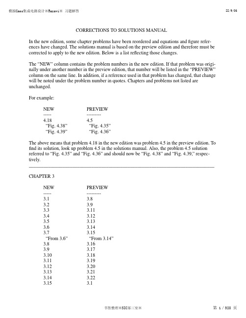
CORRECTIONS TO SOLUTIONS MANUALIn the new edition, some chapter problems have been reordered and equations and figure refer-ences have changed. The solutions manual is based on the preview edition and therefore must be corrected to apply to the new edition. Below is a list reflecting those changes.The “NEW” column contains the problem numbers in the new edition. If that problem was origi-nally under another number in the preview edition,that number will be listed in the“PREVIEW”column on the same line.In addition,if a reference used in that problem has changed,that change will be noted under the problem number in quotes. Chapters and problems not listed are unchanged.For example:NEW PREVIEW--------------4.18 4.5“Fig. 4.38” “Fig. 4.35”“Fig. 4.39” “Fig. 4.36”The above means that problem4.18in the new edition was problem4.5in the preview edition.To find its solution, look up problem 4.5 in the solutions manual. Also, the problem 4.5 solution referred to “Fig. 4.35” and “Fig. 4.36” and should now be “Fig. 4.38” and “Fig. 4.39,” respec-tively._____________________________________________________________________________ CHAPTER 3NEW PREVIEW--------------3.1 3.83.2 3.93.3 3.113.4 3.123.5 3.133.6 3.143.7 3.15“From 3.6” “From 3.14”3.8 3.163.9 3.173.10 3.183.11 3.193.12 3.203.13 3.213.14 3.223.15 3.13.16 3.23.17 3.2’3.18 3.33.19 3.43.20 3.53.21 3.63.22 3.73.23 3.103.24 3.233.25 3.243.26 3.253.27 3.263.28 3.273.29 3.28 CHAPTER 4NEW PREVIEW--------------4.1 4.124.2 4.134.3 4.144.4 4.154.5 4.164.6 4.174.7 4.18“p. 4.6” “p. 4.17”4.8 4.194.9 4.204.10 4.214.11 4.224.12 4.234.13 4.24“p. 4.9” “p. 4.20”4.14 4.1“(4.52)” “(4.51)”“(4.53)” “(4.52)”4.15 4.24.16 4.34.17 4.44.18 4.5“Fig. 4.38” “Fig. 4.35”“Fig. 4.39” “Fig. 4.36”4.19 4.6“Fig 4.39(c)” “Fig 4.36(c)”4.20 4.74.21 4.84.22 4.94.23 4.104.24 4.114.25 4.254.26 4.26“p. 4.9” “p. 4.20”CHAPTER 5NEW PREVIEW--------------5.1 5.165.2 5.175.3 5.185.4 5.195.5 5.205.6 5.215.7 5.225.8 5.235.9 5.15.10 5.25.11 5.35.12 5.45.13 5.55.14 5.65.15 5.75.16 5.85.17 5.95.18 5.10“Similar to 5.18(a)” “Similar to 5.10(a)”5.19 5.115.20 5.125.21 5.135.22 5.145.23 5.15CHAPTER 6NEW PREVIEW--------------6.1 6.76.2 6.86.3 6.9“from eq(6.23)” “from eq(6.20)”6.4 6.106.5 6.11“eq (6.52)” “eq (6.49)”6.6 6.16.7 6.26.8 6.36.9 6.46.10 6.56.11 6.66.13 6.13“eq (6.56)” “eq (6.53)”“problem 3” “problem 9”6.16 6.16“to (6.23) & (6.80)” “to (6.20) & (6.76)”6.17 6.17“equation (6.23)” “equation (6.20)”CHAPTER 7NEW PREVIEW--------------7.27.2“eqn. (7.59)” “eqn. (7.57)”7.177.17“eqn. (7.59)” “eqn. (7.57)7.197.19“eqns 7.66 and 7.67” “eqns 7.60 and 7.61”7.217.21“eqn. 7.66” “eqn. 7.60”7.227.22“eqns 7.70 and 7.71” “eqns. 7.64 and 7.65”7.237.23“eqn. 7.71” “eqn. 7.65”7.247.24“eqn 7.79” “eqn 7.73”CHAPTER 8NEW PREVIEW--------------8.18.58.28.68.38.78.48.88.58.98.68.108.78.118.88.18.98.28.108.38.118.48.138.13“problem 8.5” “problem 8.9”CHAPTER 13NEW PREVIEW--------------3.17 3.17“Eq. (3.123)” “Eq. (3.119)”CHAPTER 14 - New Chapter, “Oscillators”CHAPTER 15 - New Chapter, “Phase-Locked Loops”CHAPTER 16 - Was Chapter 14 in Preview Ed.Change all chapter references in solutions manual from 14 to 16. CHAPTER 17 - Was Chapter 15 in Preview Ed.Change all chapter references in solutions manual from 15 to 17. CHAPTER 18 - Was Chapter 16 in Preview Ed.NEW PREVIEW--------------18.316.3“Fig. 18.12(c)” “Fig. 16.13(c)”18.816.8“Fig. 18.33(a,b,c,d)” “Fig. 16.34(a,b,c,d)”Also, change all chapter references from 16 to 18.。
- 1、下载文档前请自行甄别文档内容的完整性,平台不提供额外的编辑、内容补充、找答案等附加服务。
- 2、"仅部分预览"的文档,不可在线预览部分如存在完整性等问题,可反馈申请退款(可完整预览的文档不适用该条件!)。
- 3、如文档侵犯您的权益,请联系客服反馈,我们会尽快为您处理(人工客服工作时间:9:00-18:30)。
AV
Vout Vin
RD nCox
W L
RD (Vin
VTH )
gm RD
gm or RD , then AV
Single-Stage Amplifiers
common-source with resistive load (4) : Large-signal
analysis
Since:
gm
Develop intuitive (直观的)techniques and models useful in understanding complex systems. Use proper approximations so as to create a simple mental picture of a complicated circuit, and makes it possible to formulate the behavior of most circuits by inspection rather than by lengthy calculations.
L arge signal analysis : Vin1 :Vin Vout VTH Threshold of saturationand triode
Small-signal analysis
Single-Stage Amplifiers
common-source with resistive load (2): Large-signal
Single-Stage Amplifiers
Basic concepts (2)
For small signal increment x, if we have:
y 1x
We call this amplifier a linear amplifier
In fact, due to the noise and distortion etc., the amplifier is usually not exactly a linear amplifier. So we use a concept of “Linearity” to reveal how this amplifier is more close to a linear amplifier.
common-source with resistive load (3): Small-signal
analysis
The current and transconductance approch for M1:
gm
I D Vin
Vin1 :Vin Vout VTH
If M1 is in saturation region, small-signal gain:
Single-Stage Amplifiers
Basic concepts (1)
The input-output characteristics of an amplifier is a nonlinear function (Taylor expansion, 泰勒展开):
y(t) 0 1x(t) 2 x2 (t) n xn (t) x1 x x2
Single-Stage Amplifiers
overview
Study low-frequency behavior of single-stage CMOS amplifiers including:
Common-source Source follower Common-gate Cascode configurations
Single-Stage Amplifiers
common-source (共源) with resistive load (1)
❖ Large-signal analysis for bias selection; ❖ While small-signal analysis for amplification
Single-Stage Amplifiers
Basic concepts (3)
Besides Linearity, there are some other figures needed to be considered when we design an analog integrated circuit. Below is an “analog design octagon (八边形规则)” to show the analog design compromise (折衷):
2ID Vin VTH
and in practical design, the overdrive voltage Vin-VTH is limited by
voltage slew rate (压摆率):
gm ID power
Vout
VDD
RD
1 2
nCox
W L
2(Vin VTH )Vout Vout 2
When Vin is high enough, M1 is in linear (deep triode) region:
Vout
VDD
Ro
RD (Vin
VTH )
Single-Stage Amplifiers
analysis
When 0Vin <VTH:
M1 is off and Vout=VDD
When VTH Vin <Vout +VTH, M1 is in saturation region:
Vout
VDD
RD
1 2
nCox
W L
(Vin
VTH
)2
When Vin > Vout + VTH, M1 is in triode region:
For small range of x, above function can be simplified as:
y(t) 0 1x(t)
Where 0 can be considered the bias point(偏置) and 1 the small-signal gain (小信号增益)